General Description
The MAX3040MAX3045 is a family of 5V quad RS-
485/RS-422 transmitters designed for digital data trans-
mission over twisted-pair balanced lines. All transmitter
outputs are protected to ±10kV using the Human Body
Model. In addition the MAX3040MAX3045 withstand
±4kV per IEC 1000-4-4 Electrical Fast Transient/Burst
Stressing. The MAX3040/MAX3043 (250kbps) and the
MAX3041/MAX3044 (2.5Mbps) are slew-rate limited
transmitters that minimize EMI and reduce reflections
caused by improperly terminated cables, thus allowing
error-free transmission.
The MAX3040MAX3045 feature a hot-swap capability*
that eliminates false transitions on the data cable during
power-up or hot insertion. The MAX3042B/MAX3045B
are optimized for data transfer rates up to 20Mbps, the
MAX3041/MAX3044 for data rates up to 2.5Mbps, and
the MAX3040/MAX3043 for data rates up to 250kbps.
The MAX3040MAX3045 offer optimum performance
when used with the MAX3093E or MAX3095 5V quad
differential line receivers or MAX3094E/MAX3096 3V
quad differential line receivers.
The MAX3040MAX3045 are ESD-protected pin-compat-
ible, low-power upgrades to the industry-standard
`SN75174 and `DS26LS31C. They are available in space-
saving TSSOP, narrow SO, and wide SO packages.
*Patent pending
Applications
Telecommunications Equipment
Industrial Motor Control
Transmitter for ESD-Sensitive Applications
Hand-Held Equipment
Industrial PLCs
Networking
Features
o ESD Protection: ±10kV--Human Body Model
o Single +5V Operation
o Guaranteed Device-to-Device Skew
(MAX3040/MAX3041/MAX3043/MAX3044)
o Pin-Compatible with `SN75174, `26LS31C and
LTC487
o Hot-Swappable for Telecom Applications
o Up to 20Mbps Data Rate (MAX3042B/MAX3045B)
o Slew-Rate Limited (Data Rates at 2.5Mbps and
250kbps)
o 2nA Low-Power Shutdown Mode
o 1mA Operating Supply Current
o ±4kV EFT Fast Transient Burst Immunity per IEC
1000-4-4
o Level 2 Surge Immunity per IEC 1000-4-5,
Unshielded Cable Model
o Ultra-Small 16-Pin TSSOP, 16-Pin Narrow SO, and
Wide 16-Pin SO
MAX3040MAX3045
±10kV ESD-Protected, Quad 5V RS-485/RS-422
Transmitters
________________________________________________________________ Maxim Integrated Products
1
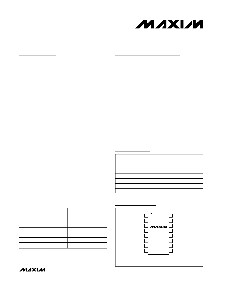
Pin Configurations
Selector Guide
Ordering Information
19-2143; Rev 1; 12/01
Ordering Information continued at end of data sheet.
For pricing, delivery, and ordering information, please contact Maxim/Dallas Direct! at
1-888-629-4642, or visit Maxim's website at www.maxim-ic.com.
PART
TEMP RANGE
PIN-PACKAGE
DATA
RATE
MAX3040CUE
0
°C to +70°C 16 TSSOP
250kbps
MAX3040CSE
0
°C to +70°C 16 Narrow SO
250kbps
MAX3040CWE
0
°C to +70°C 16 Wide SO
250kbps
MAX3040EUE
-40
°C to +85°C
16 TSSOP
250kbps
MAX3040ESE
-40
°C to +85°C
16 Narrow SO
250kbps
MAX3040EWE -40
°C to +85°C
16 Wide SO
250kbps
16
15
14
13
12
11
10
9
1
2
3
4
5
6
7
8
T1IN
V
CC
T4IN
Y4
Z4
EN34
Z3
Y3
T3IN
TOP VIEW
MAX3040
MAX3041
MAX3042B
16 TSSOP/SO
Y1
Z1
Y2
EN12
Z2
T2IN
GND
PART
DATA RATE
(bps)
INDUSTRY STANDARD
PINOUT
MAX3040
250k
75174, 34C87, LTC487
MAX3041
2.5M
75174, 34C87, LTC487
MAX3042B
20M
75174, 34C87, LTC487
MAX3043
250k
26LS31
MAX3044
2.5M
26LS31
MAX3045B
20M
26LS31
Pin Configurations continued at end of data sheet.

MAX3040MAX3045
±10kV ESD-Protected, Quad 5V RS-485/RS-422
Transmitters
2
_______________________________________________________________________________________
ABSOLUTE MAXIMUM RATINGS
ELECTRICAL CHARACTERISTICS
(V
CC
= +5V ±5%, T
A
= T
MIN
to T
MAX
, unless otherwise noted. Typical values are at V
CC
= +5V and T
A
= +25°C.) (Note 1)
Stresses beyond those listed under "Absolute Maximum Ratings" may cause permanent damage to the device. These are stress ratings only, and functional
operation of the device at these or any other conditions beyond those indicated in the operational sections of the specifications is not implied. Exposure to
absolute maximum rating conditions for extended periods may affect device reliability.
All voltages referenced to ground (GND).
Supply Voltage (V
CC
).............................................................+7V
Control Input Voltage (EN, EN, EN_) .........-0.3V to (V
CC
+ 0.3V)
Driver Input Voltage (T_IN).........................-0.3V to (V
CC
+ 0.3V)
Driver Output Voltage (Y_, Z_)
(Driver Disabled) .............................................-7.5V to +12.5V
Driver Output Voltage (Y_, Z_)
(Driver Enabled) .................................................-7.5V to +10V
Continuous Power Dissipation (T
A
= +70°C)
16-Pin TSSOP (derate 9.4mW/°C above +70°C) ..........755mW
16-Pin Narrow SO (derate 8.70mW/°C above +70°C) ..696mW
16-Pin Wide SO (derate 9.52mW/°C above +70°C) .....762mW
Operating Temperature Range
MAX304_C_E .......................................................0°C to +70°C
MAX304_E_E ....................................................-40°C to +85°C
Maximum Junction Temperature .....................................+150°C
Storage Temperature Range .............................-65°C to +150°C
Lead Temperature (soldering, 10s) .................................+300°C
PARAMETER
SYMBOL
CONDITIONS
MIN
TYP
MAX
UNITS
DRIVER
Figure 1, R = 50
2.0
Driver Differential Output
V
OD
Figure 1, R = 27
1.5
V
Change in Magnitude of
Differential Output Voltage
V
OD
Figure 1, R = 50
or 27 (Note 2)
0.2
V
Driver Common-Mode Output
Voltage
V
OC
Figure 1, R = 50
or 27
V
CC
/ 2
3
V
Change In Magnitude of
Common-Mode Voltage
V
OC
Figure 1, R = 50
or 27 (Note 2)
0.2
V
Input High Voltage
V
IH
T_IN, EN_, EN, EN
2.0
V
Input Low Voltage
V
IL
T_IN, EN_, EN, EN
0.8
V
Hot-Swap Driver Input Current
I
HOT
SWAP
EN_, EN, EN (Note 3)
±200
µA
Driver Input Current
I
IN
T_IN, EN_, EN, EN
±1
µA
Driver Short-Circuit Output
Current
I
SC
-7V
<
VOUT
<
+10V (Note 4)
±25
±250
mA
MAX3040/MAX3041/MAX3042B
EN_ = GND
Output Leakage (Y_, Z_)
when Disabled
MAX3043/MAX3044/MAX3045B
EN = GND, EN = V
CC
±1
µA
ESD Protection (Y_, Z_)
Human Body Model
±10
kV
Electrical Fast Transient/Burst
Immunity
IEC 1000-4-4
±4
kV
SUPPLY CURRENT
Supply Current
I
CC
No load
1
2
mA
MAX3040/MAX3041/MAX3042B
EN_ = GND, T
A
= +25°C
Supply Current in Shutdown
Mode
I
SHDN
MAX3043/MAX3044/MAX3045B
EN = GND, EN = V
CC
, T
A
= +25°C
0.002
10
µA
MAX3040MAX3045
±10kV ESD-Protected, Quad 5V RS-485/RS-422
Transmitters
_______________________________________________________________________________________
3
SWITCHING CHARACTERISTICS--MAX3040/MAX3043
(V
CC
= +5V ±5%, T
A
= T
MIN
to T
MAX
, unless otherwise noted. Typical values are at V
CC
= +5V and T
A
= +25°C.)
PARAMETER
SYMBOL
CONDITIONS
MIN
TYP
MAX
UNITS
Maximum Data Rate
f
MAX
250
kbps
t
PLH
0.7
1.5
Driver Propagation Delay
t
PHL
Figures 2 and 3,
R
DIFF
= 54
, C
DIFF
= 50pF
0.7
1.5
µs
t
F
0.48
0.75
1.33
Driver Differential Output
Rise-Time/Fall-Time
t
R
Figures 2 and 3,
R
DIFF
= 54
, C
DIFF
= 50pF
0.48
0.75
1.33
µs
t
DSKEW
Different chips
±350
Skew Driver to Driver
t
SSKEW
Same chip
Figures 2 and 3,
R
DIFF
= 54
,
C
DIFF
= 50pF
±100
ns
Driver Differential Output Skew
| tPLH - t PHL |
t
SKEW
Figures 2 and 3,
R
DIFF
= 54
, C
DIFF
= 50pF
±100
ns
Driver Enable to Output High
t
ZH
MAX3040, Figures 4 and 5, S2 closed,
R
L
= 500
, C
L
= 100pF
2.0
µs
Driver Enable from Shutdown to
Output High
t
ZH(SHDN)
Figures 4 and 5, S2 closed,
R
L
= 500
, C
L
= 100pF
2.0
µs
Driver Enable to Output Low
t
ZL
MAX3040, Figures 4 and 5, S1 closed,
R
L
= 500
, C
L
= 100pF
2.0
µs
Driver Enable from Shutdown to
Output Low
t
ZL(SHDN)
Figures 4 and 5, S1 closed,
R
L
= 500
, C
L
= 100pF
2.0
µs
Driver Disable Time from Low
t
LZ
Figures 4 and 5, S1 closed,
R
L
= 500
, C
L
= 15pF
500
ns
Driver Disable Time from High
t
HZ
Figures 4 and 5, S2 closed,
R
L
= 500
, C
L
= 15pF
500
ns
SWITCHING CHARACTERISTICS--MAX3041/MAX3044
(V
CC
= +5V ±5%, T
A
= T
MIN
to T
MAX
, unless otherwise noted. Typical values are at V
CC
= +5V and T
A
= +25°C.)
PARAMETER
SYMBOL
CONDITIONS
MIN
TYP
MAX
UNITS
Maximum Data Rate
f
MAX
2.5
Mbps
t
PLH
70
150
Driver Propagation Delay
t
PHL
Figures 2 and 3,
R
DIFF
= 54
, C
DIFF
= 50pF
70
150
ns
t
F
33
70
133
Driver Differential Output
Rise-Time/Fall-Time
t
R
Figures 2 and 3,
R
DIFF
= 54
, C
DIFF
= 50pF
33
70
133
ns
t
DSKEW
Different chips
±52
Skew Driver to Driver
t
SSKEW
Same chip
Figures 2 and 3,
R
DIFF
= 54
,
C
DIFF
= 50pF
±15
ns
Driver Differential Output Skew
| tPLH - t PHL |
t
SKEW
Figures 2 and 3,
R
DIFF
= 54
, C
DIFF
= 50pF
±15
ns
Driver Enable to Output High
t
ZH
MAX3041, Figures 4 and 5, S2 closed,
R
L
= 500
, C
L
= 100pF
400
ns

MAX3040MAX3045
±10kV ESD-Protected, Quad 5V RS-485/RS-422
Transmitters
4
_______________________________________________________________________________________
Note 1: All currents into the device are positive; all currents out of the device are negative. All voltages are referenced to device
ground unless otherwise noted.
Note 2:
V
OD
and
V
OC
are the changes in V
OD
and V
OC
, respectively, when the transmitter input changes state.
Note 3: This input current level is for the hot-swap enable (EN_, EN, EN) inputs and is present until the first transition only. After the
first transition the input reverts to a standard high-impedance CMOS input with input current I
IN
. For the first 20µs the input
current may be as high as 1mA. During this period the input is disabled.
Note 4: Maximum current level applies to peak current just prior to foldback-current limiting. Minimum current level applies during
current limiting.
SWITCHING CHARACTERISTICS--MAX3041/MAX3044 (continued)
(V
CC
= +5V ±5%, T
A
= T
MIN
to T
MAX
, unless otherwise noted. Typical values are at V
CC
= +5V and T
A
= +25°C.)
SWITCHING CHARACTERISTICS--MAX3042B/MAX3045B
(V
CC
= +5V ±5%, T
A
= T
MIN
to T
MAX
, unless otherwise noted. Typical values are at V
CC
= +5V and T
A
= +25°C.)
PARAMETER
SYMBOL
CONDITIONS
MIN
TYP
MAX
UNITS
Maximum Data Rate
f
MAX
20
Mbps
t
PLH
23
40
Driver Propagation Delay
t
PHL
Figures 2 and 3,
R
DIFF
= 54
, C
DIFF
= 50pF
23
40
ns
t
F
17
Driver Differential Output
Rise-Time/Fall-Time
t
R
Figures 2 and 3,
R
DIFF
= 54
, C
DIFF
= 50pF
17
ns
t
DSKEW
Different chips
±8
Skew Driver to Driver
t
SSKEW
Same chip
Figures 2 and 3,
R
DIFF
= 54
,
C
DIFF
= 50pF
±8
ns
Differential Driver Output Skew
| t
PLH
- t
PHL
|
t
SKEW
Figures 2 and 3,
R
DIFF
= 54
, C
DIFF
= 50pF
±8
ns
Driver Enable to Output High
t
ZH
MAX3042B, Figures 4 and 5, S2 closed,
R
L
= 500
, C
L
= 100pF
300
ns
Driver Enable from Shutdown to
Output High
t
ZH(SHDN)
Figures 4 and 5, S2 closed,
R
L
= 500
, C
L
= 100pF
300
ns
Driver Enable to Output Low
t
ZL
MAX3042B, Figures 4 and 5, S1 closed,
R
L
= 500
, C
L
= 100pF
300
ns
Driver Enable from Shutdown to
Output Low
t
ZL(SHDN)
Figures 4 and 5, S1 closed,
R
L
= 500
, C
L
= 100pF
300
ns
Driver Disable Time from Low
t
LZ
Figures 4 and 5, S1 closed,
R
L
= 500
, C
L
= 15pF
400
ns
Driver Disable Time from High
t
HZ
Figures 4 and 5, S2 closed,
R
L
= 500
, C
L
= 15pF
400
ns
PARAMETER
SYMBOL
CONDITIONS
MIN
TYP
MAX
UNITS
Driver Enable from Shutdown to
Output High
t
ZH(SHDN)
Figures 4 and 5, S2 closed,
R
L
= 500
, C
L
= 100pF
400
ns
Driver Enable to Output Low
t
ZL
MAX3041, Figures 4 and 5, S1 closed,
R
L
= 500
, C
L
= 100pF
400
ns
Driver Enable from Shutdown to
Output Low
t
ZL(SHDN)
Figures 4 and 5, S1 closed,
R
L
= 500
, C
L
= 100pF
400
ns
Driver Disable Time from Low
t
LZ
Figures 4 and 5, S1 closed,
R
L
= 500
, C
L
= 15pF
500
ns
Driver Disable Time from High
t
HZ
Figures 4 and 5, S2 closed,
R
L
= 500
, C
L
= 15pF
500
ns
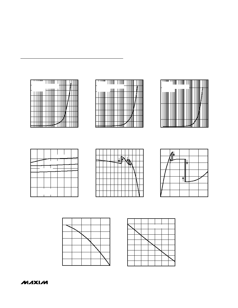
MAX3040 toc06
OUTPUT LOW VOLTAGE (V)
OUTPUT CURRENT (mA)
5
4
-6 -5 -4
-2 -1 0
1
2
-3
3
10
20
30
40
50
60
70
80
0
-7
6
OUTPUT CURRENT vs. TRANSMITTER
OUTPUT HIGH VOLTAGE
0.7
0.8
1.0
0.9
1.1
1.2
0
20
10
30
40
50
60
70
SUPPLY CURRENT vs. TEMPERATURE
MAX3040 toc04
TEMPERATURE (
°C)
SUPPLY CURRENT (mA)
V
CC
= 5.25V
V
CC
= 5V
V
CC
= 4.75V
NO LOAD
NO SWITCHING
100
1000
0
10
5
15
20
25
35
30
40
45
0.1
1
10
MAX3040/MAX3043
SUPPLY CURRENT vs. DATA RATE
MAX3040 toc01
DATA RATE (kbps)
SUPPLY CURRENT (mA)
NO LOAD
ALL FOUR TRANSMITTERS
SWITCHING
40
0
0.1
1
10
100
1000
10,000
MAX3041/MAX3044
SUPPLY CURRENT vs. DATA RATE
MAX3040 toc02
DATA RATE (kbps)
SUPPLY CURRENT (mA)
10
5
20
15
35
30
25
NO LOAD
ALL FOUR TRANSMITTERS
SWITCHING
MAX3042B/MAX3045B
SUPPLY CURRENT vs. DATA RATE
DATA RATE (kbps)
0.1
100
1000 10,000
1
10
100,000
SUPPLY CURRENT (mA)
60
0
10
20
30
50
40
MAX3040 toc03
NO LOAD
ALL FOUR TRANSMITTERS
SWITCHING
0
20
10
40
30
60
50
70
0
4
2
6
8
10
OUTPUT CURRENT vs. TRANSMITTER
OUTPUT LOW VOLTAGE
MAX3040 toc06
OUTPUT LOW VOLTAGE (V)
OUTPUT CURRENT (mA)
MAX3040MAX3045
±10kV ESD-Protected, Quad 5V RS-485/RS-422
Transmitters
_______________________________________________________________________________________
5
Typical Operating Characteristics
(V
CC
= +5V, T
A
= +25°C, unless otherwise noted.)
0
20
10
40
30
60
50
70
0
2
1
3
4
5
OUTPUT CURRENT
vs. DIFFERENTIAL OUTPUT VOLTAGE
MAX3040 toc07
DIFFERENTIAL OUTPUT VOLTAGE (V)
OUTPUT CURRENT (mA)
2.10
2.20
2.15
2.35
2.30
2.25
2.50
2.45
2.40
2.55
0
20
30
10
40
50
60
70
TRANSMITTER DIFFERENTIAL OUTPUT
VOLTAGE vs. TEMPERATURE
MAX3040 toc08
TEMPERATURE (
°C)
DIFFERENTIAL OUTPUT VOLTAGE (V)
R
DIFF
= 54