
For free samples & the latest literature: http://www.maxim-ic.com, or phone 1-800-998-8800.
For small orders, phone 1-800-835-8769.
________________General Description
The MAX2430EVKIT-SO and MAX2430EVKIT-QSOP eval-
uation kits (EV kits) simplify evaluation of the MAX2430 sili-
con RF power amplifier. They enable testing of all
MAX2430 functions over the 800MHz to 950MHz band,
with no additional support circuitry and with minimal
equipment.
To evaluate the MAX2430 in the SO package
(MAX2430ISE), order the MAX2430EVKIT-SO. To evaluate
the MAX2430 in the PwrQSOP package, order the
MAX2430EVKIT-QSOP. These are surface-mount packages.
____________________________Features
o
Low-Cost, Silicon RF Power Amplifier
o
Delivers More than 125mW Output Power from
+3.6V Supply
o
Single +3V to +5.5V Supply Range, Ideal for 3-Cell
NiCd or 1-Cell Lithium-Ion Battery Operation
o
Output Matching Network is Tunable from
800MHz to 950MHz
o
TTL/CMOS-Compatible Shutdown Input
o
Easy Testing of All MAX2430 Features
o
Fully Assembled and Tested Surface-Mount
Package
Evaluate: MAX2430
MAX2430 Evaluation Kits
________________________________________________________________
Maxim Integrated Products
1
QTY
DESCRIPTION
C1¡C5
5
C6
1
C7
1
1ÁF, 10V, 10% tantalum capacitor SMT
AVX TAJA105K016
CO, CSH
2
L1, L2
2
8nH, 10% spring inductors
Coilcraft A03T
LC
1
RC
1
U1
1
VCC, GND
2
Supply connectors
J1
1
3-pin header
None
1
Shunt
0pF to 6pF SMT trimmer capacitors
Voltronics JR060
2.2nF, 10% ceramic chip capacitor
(0805)
1nF, 10% ceramic chip capacitors
(0805)
SUPPLIER
PHONE
FAX
AVX
(803) 946-0690
(803) 626-3123
______________Component Suppliers
DESIGNATION
47nH, 20% inductor
Coilcraft 0805CS-470XMBC
470
, 5% resistor (0805)
MAX2430ISE
______________________________________________________________Component List
_______________Ordering Information
Coilcraft
(847) 639-6400
(847) 639-1469
Sprague
(603) 224-1961
(603) 224-1430
Voltronics
(201) 586-8585
(201) 586-3404
PIN, POUT
2
SMA connectors
DESIGNATION QTY
DESCRIPTION
C1¡C5
5
1nF, 10% ceramic chip capacitors
(0603)
C6
1
2.2nF, 10% ceramic chip capacitor
(0603)
C7
1
1ÁF, 10V, 10% tantalum capacitor SMT
AVX TAJA105K016
C
O
, C
SH
2
0pF to 6pF SMT trimmer capacitors
Voltronics JR060
L1
1
8nH, 10% spring inductor
Coilcraft A03T
LC
1
47nH, 20% inductor
Coilcraft 0805CS-470XMBC
RC
1
470
, 5% resistor (0603)
U1
1
MAX2430IEE
VCC, GND
2
Supply connectors
J1
1
3-pin header
None
1
Shunt
PIN, POUT
2
SMA connectors
L2
1
12nH, 10% spring inductor
Coilcraft A04T
MAX2430EVKIT-SO
MAX2430EVKIT-PwrQSOP
PART
MAX2430EVKIT-PwrQSOP
0░C to +70░C
TEMP. RANGE
IC PACKAGE
16 PwrQSOP
19-1093; Rev 2; 1/98
MAX2430EVKIT-SO
0░C to +70░C
16 Narrow SO

_________________________Quick Start
The MAX2430 EV kits are fully assembled and factory
tested. All measurements described below use a
900MHz test frequency.
Do not turn on the power
until all connections are made.
Test Equipment Required
À Signal-Source Sine-Wave Generator with range up to
1000MHz (example: HP8656B)
À Spectrum Analyzer with range up to 4GHz (example:
TEK2755AP)
À +3V to +5.5V, 400mA adjustable output power sup-
ply
À Current meter that can display up to 400mA
Connections and Signal Conditions
1) Connect an SMA cable from the RF signal source to
the PIN input on the EV kit. Ensure that the RF power-
source input power is off or set below -50dBm.
2) Connect an SMA cable from the spectrum analyzer
to the POUT connector on the EV kit. Note that if the
front end of the spectrum analyzer can not handle
more than 20dBm of input power, you must place an
appropriate attenuator between the POUT connector
and the spectrum analyzer to prevent damage.
3) Connect the 3V power supply through a current
meter to the appropriate VCC and GND terminals on
the EV kit, and apply power.
4) Position the J1 shunt across pins 1 and 2 to enable
the MAX2430 (SHDN = high). Note that the normal
bias current drawn by the MAX2430 EV kit should be
approximately 30mA to 60mA over the 3V to 5.5V
supply range when no RF input power is applied.
5) Set the input power to -20dBm and the frequency to
900MHz on the signal source.
6) Set the spectrum analyzer's dynamic range and fre-
quency range for an appropriate setting to view the
900MHz output.
7) Tune the output stage matching network for maximum
output power at 900MHz. See the
Adjustments and
Control section for the C
O
and C
SH
trim-capacitor tun-
ing procedure
_______________Detailed Description
Analysis
1) Set the RF source power to -13dBm. At 900MHz, the
spectrum analyzer should display a power level near
20dBm (of course, if you have used an attenuator,
adjust your reading accordingly). If necessary, adjust
the input power up or down in 0.1dB steps to get the
equivalent output power equal to 20dBm at the POUT
port. The power gain (G
P
= P
OUT
- P
IN
) should be
greater than 30dB.
If you cannot achieve 20dBm output power, verify
that the supply voltage between the V
CC
and GND
pads on the EV kit is 3.00V. This ensures that the
supply connection wire and current-meter shunt
losses are not causing excessive supply voltage
drops. Also, make sure the output stage matching
network has been properly tuned for the center fre-
quency of interest, according to the C
O
and C
SH
trim-capacitor tuning procedure found in the
Adjustments and Control section.
2) Disable the MAX2430 by moving the J1 shunt to
pins 2 and 3. With the part disabled and RF power
still applied to the RF input, you can measure the off-
state feedthrough of the MAX2430. Adjust your
spectrum analyzer to display the amount of 900MHz
leakage power that exists at the POUT port. The iso-
lation should be approximately 50dB, so with an
input power of -12dBm, the output power should
measure approximately -62dBm.
3) Enable the MAX2430 again by moving the J1 shunt
to pins 1 and 2. Note that the output power is again
around 20dBm.
4) Set the spectrum analyzer to display the 1800MHz
2nd harmonic frequency. The measured power
should be typically 26dB down from the fundamental
power at 900MHz. The 3rd harmonic power at
2700MHz should be typically 40dB down. The three-
element output stage matching circuitry provides
some rejection of the harmonic products.
5) Set the spectrum analyzer to measure the 900MHz
fundamental power. Adjust V
CC
from 3V up to 5.5V.
Note that the output power has risen approximately
2dBm (up to 22dBm) and that the power gain has
increased by 2dB.
Adjustments and Control
C
O
and C
SH
The quickest method for tuning the output is to apply
-20dBm of input power at the desired frequency, then
adjust C
O
and C
SH
until the output power is maximized
as read from a spectrum analyzer or power-meter dis-
play. Only one value of C
O
and C
SH
is correct for a
given frequency. For best results, use a nonconductive
adjustment tool.
CO and CSH are surface-mount, 0pF to 6pF trim
capacitors used to tune the output transistor matching
Evaluate: MAX2430
MAX2430 Evaluation Kits
2
_______________________________________________________________________________________

network to 50
. This ensures maximum power transfer
and good output VSWR at any selected narrow-band
frequency range of interest between 800MHz and
950MHz. The open-collector output transistor (RFOUT
pin) should see approximately a 15
internal load
impedance to achieve maximum power gain with the
best efficiency. The internal package inductance (5nH),
L1 (8nH), series capacitor C
O
, and shunt capacitor
C
SH
form a 15
to 50
tuneable matching network.
Resistor R
C
enhances stability under load mismatch
conditions and does not affect normal operation of the
circuit. The 47nH supply choke (labeled L
C
) provides
DC bias.
Shutdown Control
The SHDN pin is TTL/CMOS compatible and is used to
enable (or disable) the MAX2430. Table 1 lists the
options available for the shutdown control jumper, J1.
To use an external control signal, remove the shunt on
J1 completely, and connect the external signal to the
pad marked SHDN. The external control signal should
not exceed V
CC
. Supply current in the disabled mode
is typically less than 1ÁA.
BIAS Pin
The BIAS pin regulates the ramp-up and ramp-down times
of the output RF envelope. It can also be driven externally
to control the output power over a 15dB range. The ramp-
up/down slope is set by a capacitor connected from the
BIAS pin to ground. The EV kit comes with a 2.2nF capaci-
tor (C6), which yields an RF envelope ramp-up/down time
of approximately 10Ás. The BIAS pad on the EV kit allows
the user to manipulate the MAX2430 BIAS pin. Refer to the
BIAS Pin section of the MAX2430 data sheet for more
information on output power control.
Layout Considerations
The evaluation board can serve as a guide for board lay-
out. Grounding is critical for the proper operation and sta-
bility of the MAX2430. The following considerations were
taken into account on the evaluation board. C1, C2, and
C3 should be small surface-mount capacitors, placed
directly from each effective V
CC
terminal to the ground
plane. Make connections short (not through vias or long
traces). C5 and C6 should be surface-mount capacitors,
located as close to the MAX2430 as possible for best
results. C2 should be next to L2. C3 should be next to L
C
.
L
C
should be perpendicular to L1, and L1 perpendicular
to L2 to ensure minimal coupling.
The evaluation board has four layers made from FR4
(
R
= 4.0 to 4.6) with 1oz. copper. The first two layers
(signal and ground planes) are 14 mils apart, which pro-
vides a 50
characteristic impedance from 25mil-wide
traces. These trace widths are used for P
IN
and P
OUT
to
maintain a 50
environment out to the SMA connectors.
The third layer is used for the V
CC
supply plane. The
fourth layer is used for the SHDN pin jumper connections
and BIAS pin signal routing. The ground metal, connect-
ed with vias on the first and second layers, acts as a
heatsink for the MAX2430, reducing internal operating
temperatures. Note that all ground and V
CC
plane is
removed under matching components (L1, L2, L
C
, R
C
,
C
O
, C
SH
) to minimize parasitic capacitance.
The MAX2430EVKIT-QSOP includes two large holes
under the MAX2430 to aid in attachment and removal of
the part. These holes are not necessary for proper circuit
operation.
Operation Outside the
800MHz to 950MHz Frequency Band
With minor modifications to the MAX2430 EV kit match-
ing network components, the operating frequency can
be tuned to frequencies outside the specified band.
Refer to the
Applications Information section of the
MAX2430 data sheet for more information.
Evaluate: MAX2430
MAX2430 Evaluation Kits
_______________________________________________________________________________________
3
Table 1. Jumper J1 Functions
SHUNT
LOCATION
SHDN PIN
MAX2430 STATUS
1 & 2
Connected to V
CC
Enabled
2 & 3
Connected to GND
Disabled

Figure 2. MAX2430 EVKIT-SO Component Placement Guide--
Component Side
Figure 3. MAX2430 EVKIT-SO PC Board Layout--
Component Side
Evaluate: MAX2430
MAX2430 Evaluation Kits
4
_______________________________________________________________________________________
MAX2430
OUTPUT
BIAS
GAIN
50
GND2
GND3
VCC1
VCC
V
CC
5nH
C3
1nF
C2
1nF
C6
2.2nF
C4
1nF
VCC2
BIAS
GND4
RFOUT
C
O
AND C
SH
TUNED FOR MAXIMUM POWER OUTPUT AT THE
DESIRED FREQUENCY BETWEEN 800MHz AND 950MHz.
9
1, 15, 16
11, 12, 13, 14
8
10
7
J1
2
6
4
3, 5
L
C
47nH
L2*
C
SH
0pF to 6pF
C
O
0pF to 6pF
L1
8nH
SHDN
GND1
1 2 3
RFIN
PIN
SMA
SMA
C5
1nF
DRIVER
SHDN
MASTER
BIAS
50
~15
C7
1
Á
F
10V
C1
1nF
P
OUT
GND
BIAS
R
C
470
L2 = 8nH FOR NARROW SO PACKAGE (MAX2430ISE)
L2 = 12nH FOR PwrQSOP PACKAGE (MAX2430IEE)
*
Figure 1. MAX2430 EV Kit Schematic
1.0"
1.0"
Evaluate: MAX2430
MAX2430 Evaluation Kits
_______________________________________________________________________________________
5
Figure 4. MAX2430 EVKIT-SO PC Board Layout--
Solder Side
Figure 5. MAX2430 EVKIT-SO PC Board Layout--Ground
Plane
1.0"
1.0"
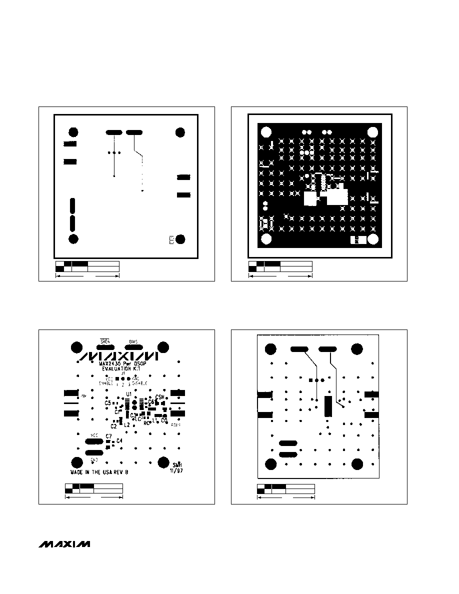
Figure 6. MAX2430 EV Kit-PwrQSOP Component Placement
Guide--Component Side
Figure 7. MAX2430 EV Kit-PwrQSOP PC Board Layout--
Solder Side
1.0"
1.0"