________________General Description
The MAX2420/MAX2421/MAX2422/MAX2460/MAX2463
evaluation kits (EV kits) simplify evaluation of the
MAX2420/MAX2421/MAX2422/MAX2460/MAX2463
900MHz image-reject transceivers.
The EV kits provide 50
SMA connectors for all RF
inputs and outputs. A varactor-based tank circuit is pro-
vided for the on-chip voltage-controlled oscillator (VCO)
and can be tuned by a potentiometer or external volt-
age. The VCO can be overdriven by an external source,
if desired. (See EXT LO Input under the
Adjustments
and Control section).
Switches are provided to control power-management
features.
____________________________Features
o
50
SMA Ports for Testing Transmit and Receive
Paths
o
SMA Port for Prescaler Output
o
Switches Included to Control Power-Management
Features
o
VCO Frequency, Receiver Gain, and Transmitter
Gain Adjustable via On-Board Potentiometers or
External Inputs
o
Fully Assembled and Tested
Evaluate: MAX2420/MAX2421/MAX2422/MAX2460/MAX2463
MAX2420/MAX2421/MAX2422
MAX2460/MAX2463 Evaluation Kits
________________________________________________________________
Maxim Integrated Products
1
QTY
DESCRIPTION
C1, C4, C5, C7,
C9, C10, C12,
C15, C19,
C21�C24,
C28, C32
15
C6, C14
2
0.1�F ceramic capacitors
C8, C11, C13,
C20, C25, C29,
C30, C31
8
C16
1
1000pF ceramic capacitor
C17, C18
2
3.6pF (0603) (MAX2421) � 0.1pF
D1
1
Dual-varactor diode
Alpha SMV1204-199
0.01�F ceramic capacitors
3.3pF (0603) (MAX2420) � 0.1pF
47pF ceramic capacitors
DESIGNATION
10�F, �10%, 10V tantalum capacitors
AVX TAJB106K010 or
Sprague 2930106X90010B
PART
MAX2420EVKIT-SO
-40�C to +85�C
TEMP. RANGE
BOARD TYPE
SURFACE MOUNT
DESIGNATION QTY
DESCRIPTION
JU2, JU3, JU4,
JU7, JU8
5
Shunts
L5, L7
0
Not installed
L6
1
12nH inductor
Coilcraft 0805CS-120XMBC
L8
1
18nH inductor
Coilcraft 0805CS-180XMBC
_______________________________________________________________________Ordering Information
4.0pF (0603) (MAX2421) � 0.1pF
4.0pF (0603) (MAX2422) � 0.1pF
4.0pF (0603) (MAX2460) � 0.1pF
C2, C3
2
4.7pF (0603) (MAX2463) � 0.1pF
1.8pF (0603) (MAX2420) � 0.1pF
C26
1
C27
0
Not installed
2.4pF (0603) (MAX2463) � 0.1pF
1.5pF (0603) (MAX2460) � 0.1pF
3.0pF (0603) (MAX2422) � 0.1pF
MAX2421EVKIT-SO
-40�C to +85�C
SURFACE MOUNT
MAX2422EVKIT-SO
-40�C to +85�C
SURFACE MOUNT
PART
MAX2460EVKIT-SO
MAX2463EVKIT-SO
-40�C to +85�C
SURFACE MOUNT
-40�C to +85�C
TEMP. RANGE
BOARD TYPE
SURFACE MOUNT
JU2, JU3, JU4,
JU7, JU8,
GND, VEXT,
DGND
8
2-pin headers
L1
1
22nH inductor
Coilcraft 0805CS-220XMBC
L2
1
8.2nH inductor
Coilcraft 0805CS-080XMBC
6.8nH, 5% (MAX2420)
Coilcraft 0805HS-060TJBC
L4
1
100nH inductor
Coilcraft 0805CS-101XKBC
19-1234; Rev 2; 2/99
______________________________________________________________________________Component List
3.3nH, 5% (MAX2421)
Coilcraft 0805HS-030TJBC
6.8nH, 5% (MAX2460)
Coilcraft 0805HS-060TJBC
3.3nH, 5% (MAX2422)
Coilcraft 0805HS-030TJBC
L3
1
6.8nH, 5% (MAX2463)
Coilcraft 0805HS-060TJBC
For free samples & the latest literature: http://www.maxim-ic.com, or phone 1-800-998-8800.
For small orders, phone 1-800-835-8769.
_________________________Quick Start
The MAX2420 EV kit is fully assembled and factory test-
ed.
Do not turn on the DC power and signal sources
until all connections are made.
Note:
The following discussion is based on the
MAX2420 with an IF frequency of 10.7MHz and high-
side LO injection. Refer to Table 2 in the data sheet for
the appropriate LO and IF frequencies associated with
the MAX2420/MAX2421/MAX2422/MAX2460/MAX2463.
Test Equipment Required
�
RF-signal generator capable of generating frequen-
cies up to 1GHz
�
Spectrum analyzer with frequency range at least to
3GHz, such as the HP8561
�
Power supply capable of +2.7V to +5.5V output at
100mA
Connections and Signal Conditions
1) Verify that all shunts are installed across jumpers
JU2, JU3, JU4, JU7, and JU8.
2) Verify that switch positions 1 through 5 on SW1 are
set at the "logic 0" position.
3) Set the power supply to 3.3V, and set the current
limit to 100mA.
4) Connect the power supply to the VEXT and GND
terminals on the EV kit.
5) For testing the receive path, set the signal-source
frequency to 915MHz and the power level to
-35dBm. For testing the transmit path, set the signal-
source frequency to 10.7MHz and the power level to
-0.8dBm.
Analysis
1) Turn on the on-chip oscillator by setting switch
VCOON to "logic 1." To observe the VCO frequen-
cy, set switch DIV 1 to "logic 1" (disabling the
prescaler and enabling the buffer amplifier) and
connect an SMA cable from the spectrum analyzer
to the PREOUT port. Set the VCO frequency to
925.7MHz by adjusting VCO ADJ (R3). The VCO
tuning range is typically 30MHz and may vary
slightly due to tolerances in the tank components.
2) The receive conversion gain can be evaluated by
setting switch RXON to "logic 1," applying a
915MHz signal to the RXIN port, and observing the
RXOUT port at 10.7MHz with the spectrum analyz-
er. The gain of the LNA in the receiver path can be
adjusted by varying R2.
______________Component Suppliers
Evaluate: MAX2420/MAX2421/MAX2422/MAX2460/MAX2463
MAX2420/MAX2421/MAX2422
MAX2460/MAX2463 Evaluation Kits
2
_______________________________________________________________________________________
SUPPLIER*
PHONE
FAX
Alpha Industries
(617) 935-5150
(617) 933-2359
Coilcraft
(847) 639-6400
(847) 639-1469
Sprague
(603) 224-1961
(603) 224-1430
AVX
(803) 946-0690
(803) 626-3123
_______Component List (continued)
Note:
All resistors and capacitors have 0805 footprint, unless
otherwise noted.
*
Please indicate that you are using the MAX2420/MAX2421/
MAX2422/MAX2460/MAX2463 when contacting these compo-
nent suppliers.
DESIGNATION
QTY
DESCRIPTION
R1, R2, R3
3
10k
potentiometers
R4, R5
2
1k
, 5% resistors
L9
1
82nH inductor
Coilcraft 0805CS-820XKBC
LNA GAIN,
TX GAIN,
VCO ADJ
3
1-pin headers
10
, 5% (0603) (MAX2420) resistors
15
, 5% (0603) (MAX2421) resistors
R8
1
47k
, 5% resistor
R10, R13
2
Not installed
R9, R14�R17
5
10k
, 5% resistors
R12, R19
2
301
, 1% resistors
RXIN, RXOUT,
TXOUT, TXIN,
PREOUT,
EXT LO INPUT
6
SMA connectors (PC edge mount)
MAX2420EAI, SSOP-28
SW1
1
5-position DIP switch
MAX2421EAI, SSOP-28
R18, R20
2
49.9
, 1% resistors
15
, 5% (0603) (MAX2422) resistors
15
, 5% (0603) (MAX2460) resistors
R6, R7
2
15
, 5% (0603) (MAX2463) resistors
MAX2422EAI, SSOP-28
MAX2460EAI, SSOP-28
U1
1
MAX2463EAI, SSOP-28

Note:
R12 and R18 are used as a resistive match-
ing network to present an optimum 330
imped-
ance to the RXOUT pin. This network results in a
14.2dB loss in the receiver path. Therefore, 14.2dB
must be added to the power level observed on the
spectrum analyzer to obtain the true receive output
power. For example, with LNA GAIN set at V
CC
and
the receive input level set at -35dBm, the receive
output observed on the spectrum analyzer is
approximately -27.2dBm. The true receive conver-
sion gain is -27.2 - (-35) + 14.2 = 22dB.
If desired, pads for C8, R18, C30, R12, L5, and
C20 can be used to build a custom reactive-
matching network.
3) Receive image rejection can be evaluated by
changing the receive input frequency to 936.4MHz
(while keeping the LO at 925.7MHz) and compar-
ing the output signal level against the one mea-
sured in step 2.
4) Before evaluating the transmitter, ensure that the
receiver is disabled by setting switch RXON to
"logic 0." The transmit conversion gain can be eval-
uated by setting switch TXON to "logic 1", applying
a 10.7MHz signal at -0.8dBm to the TXIN port, and
observing the TXOUT port at 915MHz with a spec-
trum analyzer. The gain of the input buffer amp in
the transmit path can be adjusted by varying R1.
Note:
R19 and R20 are used as a resistive match-
ing network to present an optimum 330
imped-
ance to the TXIN pin. This network results in a
14.2dB loss in the transmit path. Therefore, 14.2dB
must be subtracted from the signal source's power
to obtain the input power applied to the MAX2420
(-15dBm). With TX GAIN set at 2V and the transmit
input level set at -0.8dBm, the transmit output
observed on the spectrum analyzer is approximate-
ly -4dBm. The transmit conversion gain is -4 - (-15)
= 11dB.
If desired, pads for R19, R20, C11, L7, and C25
can be used to build a custom reactive-matching
network.
5) Tx image rejection can be evaluated by comparing
the desired lower sideband at 915MHz against the
unwanted upper sideband at 936.4MHz.
Adjustments and Control
VCO ADJ
The VCO frequency can be tuned by adjusting on-
board potentiometer R3. It can also be tuned by first
removing the shunt from jumper JU7 and then applying
an external voltage via the VCO ADJ terminal. The sup-
ply providing the external voltage must be properly
bypassed to minimize noise added to the LO.
LNA GAIN
The LNA gain can be adjusted using on-board poten-
tiometer R2. LNA gain control can also be accomplished
by first removing the shunt from jumper JU2 and then
applying an external voltage via the LNA GAIN terminal.
TX GAIN
The transmit buffer amp gain can be adjusted using on-
board potentiometer R1. Transmit gain control can also
be accomplished by first removing the shunt from jumper
JU3 and then applying an external voltage via the
TX GAIN terminal.
RXON and TXON
The receive and transmit sections are enabled by setting
switches RXON and TXON to "logic 1," respectively.
Since the transmit and receive sections share an LO and
an IF frequency, interference will result if both sections are
active at the same time. When testing either the receive or
transmit section, always disable the other section.
To disable all chip functions, set all switches to "logic 0."
To obtain an accurate reading of the device shutdown
current, remove the shunt from JU4 and move the V
CC
connection from the VEXT terminal to the left side of JU4.
EXT LO Input
An external LO input can be applied by making the fol-
lowing board changes:
1) Remove R6, R7, L3, L4, C2, C3, C26.
2) Add a 0.01�F capacitor in place of C27.
3) Replace R6 and R7 with 49.9
resistors.
4) Replace L3 and L4 with shorts.
5) Apply the LO signal at 0dBm to EXT LO input.
Prescaler Control
The function of PREOUT is controlled by the switches
labeled "DIV1" and "64" (Table 1).
Evaluate: MAX2420/MAX2421/MAX2422/MAX2460/MAX2463
MAX2420/MAX2421/MAX2422
MAX2460/MAX2463 Evaluation Kits
_______________________________________________________________________________________
3
PREOUT
FUNCTION
SWITCH "SW1" POSITIONS
LO buffered output
Logic 1
Don't care
Prescaler, �64
Logic 0
Logic 1
Prescaler, �65
Logic 0
Logic 0
DIV1
64
Table 1. PREOUT Function Control
Switches
Evaluate: MAX2420/MAX2421/MAX2422/MAX2460/MAX2463
MAX2420/MAX2421/MAX2422
MAX2460/MAX2463 Evaluation Kits
4
_______________________________________________________________________________________
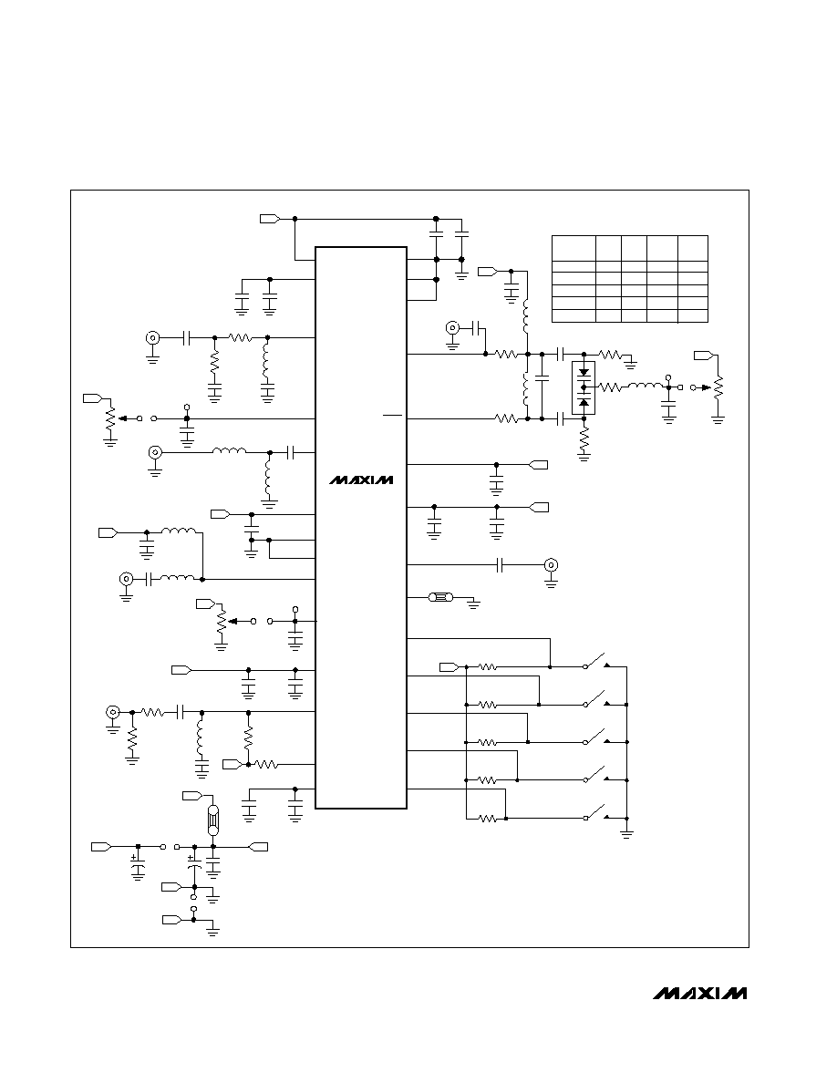
Figure 1. MAX2420 EV Kit Schematic
28
27
26
25
24
23
22
21
20
19
18
17
16
15
C28
47pF
C14
0.1
�
F
C6
0.1
�
F
VCC
C19
47
�
F
*USED FOR OTHER PRODUCT VERSIONS.
1
2
3
4
5
6
7
8
9
10
11
12
13
MAX2420
MAX2421
MAX2422
MAX2460
MAX2463
U1
C21
47pF
R1
10k
VEXT
C4
47pF
JU3
RXIN
SMA
L6
12nH
L2
8.2nH
J2
TX GAIN
C30
0.01
�
F
C20
0.01
�
F
L5
OPEN
R12
301
RXOUT
SMA
C8
0.01
�
F
J1
R18
49.9
VCC
VCC
C15
47pF
L8
18nH
L1
22nH
C10
47pF
TXOUT
SMA
J5
C5
47pF
JU6
PREOUT
SMA
J4
C12
47pF
C31
0.01
�
F
VCC2
VCC2
C32
47pF
C16
1000pF
V
CC
CAP1
RXOUT
TX GAIN
RXIN
VCC
GND
GND
TXOUT
LNA GAIN
V
CC
TXIN
N.C.
CAP2
GND
GND
GND
TANK
TANK
V
CC
V
CC
PREOUT
PREGND
MOD
DIV1
VCOON
RXON
TXON
C29
0.01
�
F
C9
47pF
C25
0.01
�
F
VCC
R13*
OPEN
C11
0.01
�
F
L7
OPEN
TXIN
SMA
J3
R19
301
R20
49.9
14
R10*
OPEN
C22
47pF
LNA
GAIN
C13
0.01
�
F
BPSK
C24
47pF
R2
10k
VEXT
JU2
VEXT
VCC2
VCC
JU4
JU5
JU8
GND
DGND
C18
10
�
F
6.3V
C17
10
�
F
6.3V
C23
47pF
VCO ADJ
C1
47pF
R3
10k
VEXT
VCC2
JU7
EXTLO
INPUT
SMA
C27
OPEN
C2
C3
C26
C7
47pF
L4
100nH
L3
D1
J13
R7
R6
R5
1k
R4
1k
L9
82nH
R8
47k
1
2
3
4
5
64
DIV1
VCOON
SW1
RXON
TXON
10
9
8
7
6
65
64/65
OFF
OFF
OFF
VEXT
R9
10k
R14
10k
R15
10k
R16
10k
R17
10k
MAX2420
MAX2421
MAX2422
MAX2460
MAX2463
PART
L3
(nH)
6.8
3.3
3.3
6.8
6.8
C26
(pF)
1.8
3.6
3.0
1.5
2.4
C2, C3
(pF)
3.3
4.0
4.0
4.0
4.7
R6, R7
(
)
10
15
15
15
15
VCO TANK COMPONENTS
FOR 915MHz TYPICAL RF
Evaluate: MAX2420/MAX2421/MAX2422/MAX2460/MAX2463
MAX2420/MAX2421/MAX2422
MAX2460/MAX2463 Evaluation Kits
_______________________________________________________________________________________
5
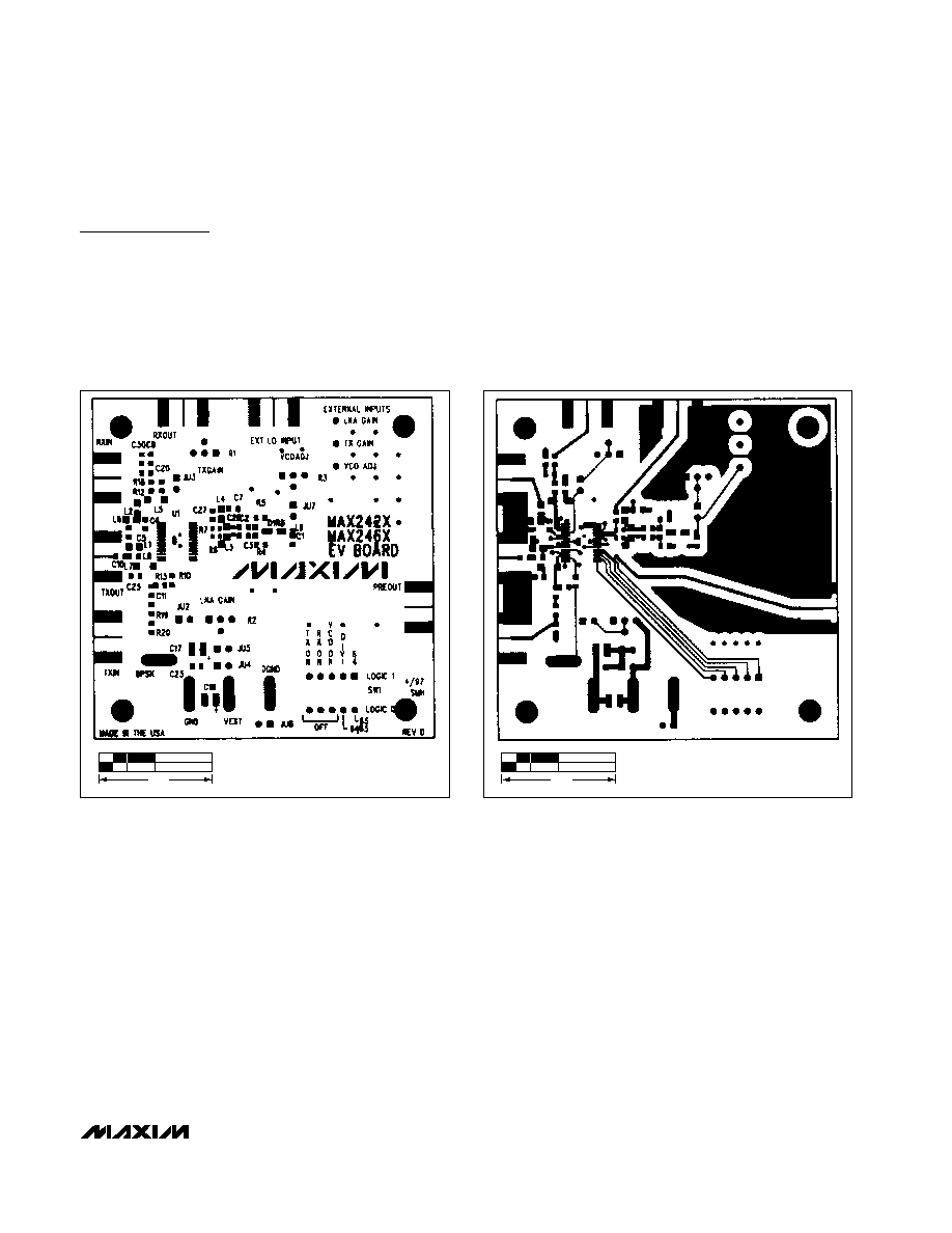
Figure 2. MAX2420 EV Kit Component Placement Guide--
Component Side
1.0"
1.0"
Figure 3. MAX2420 EV Kit PC Board Layout--Component Side
Layout Considerations
The EV board can serve as a guide for your board lay-
out. Take care in laying out the oscillator tank circuit.
Oscillation frequency is sensitive to parasitic PC board
capacitance, trace inductance, and package induc-
tance. Keep the tank layout as symmetrical, tightly
packed, and close to the device as possible to mini-
mize LO feedthrough. When using a PC board with a
ground plane, a cutout in the ground plane below the
oscillator tank reduces parasitic capacitance. Also,
keep traces carrying the receive and transmit signals
as short as possible to minimize radiation and insertion
loss due to the PC board.