General Description
The MAX2383 upconverter and PA driver IC
is designed for emerging ARIB (Japan) and
ETSI-UMTS (Europe) W-CDMA applications. The IC
includes an upconversion mixer with variable gain con-
trol, an LO buffer, and a variable-gain PA driver for out-
put power control.
The MAX2383 is designed to support the IMT-2000
frequency band. It includes a differential IF input port,
an LO input port, and PA driver input/output ports. The
upconverter mixer incorporates an AGC with over 30dB
of gain control. The IC provides automatic throttle-back
of PA driver and mixer current as output power is
reduced. The main signal path and the LO buffer can
be shutdown independently. The on-chip LO buffer can
be kept ON while the main transmitter path is being
turned on and off to minimize VCO pulling during TX
gated-transmission.
The MAX2383 is specified for +2.7V to +3.0V single
supply and is housed in an ultra-miniature 3 x 4
UCSPTM package for optimum cost- and space-reduc-
tion and for best RF performance. The IC is targeted for
the 2270MHz to 2580MHz LO frequency range. It is
fabricated using an advanced high-frequency bipolar
process. The mixer and PA driver linearity have been
optimized to provide excellent RF performance in the
1920MHz to 1980MHz band, while drawing minimal
current. The mixer's performance is optimized for a
-10dBm ±3dB LO drive at the LO buffer input port. The
LO port can be configured to be driven either single-
ended or differentially.
The MAX2383 achieves excellent noise and image sup-
pression without the use of an interstage TX SAW band-
pass filter, thereby saving valuable board space, cost,
and supply current.
For LNA and downconverter mixer companion ICs, see
the MAX2387/MAX2388/MAX2389 data sheet.
Applications
Japanese 3G Cellular Phones (ARIB)
European 3G Cellular Phones (UMTS)
Chinese 3G Cellular Phones (TD-SCDMA)
PCS Phones
Features
o +6dBm Output Power with -46dBc ACPR
o Ultra-Miniature UCSP Package
o Upconverter Gain-Control Range: 35dB
o Automatic Dynamic Current Control
o 12mA Quiescent Supply Current
o On-Chip LO Buffer with Disable
o Low Out-of-Band Noise Power in RX Band:
-144dBm/Hz at +6dBm P
OUT
o No Interstage TX SAW Bandpass Filter Required
ACTUAL SIZE
UCSP
2mm
1.5mm
MAX2383
W-CDMA Upconverter and PA Driver
with Power Control
________________________________________________________________ Maxim Integrated Products
1
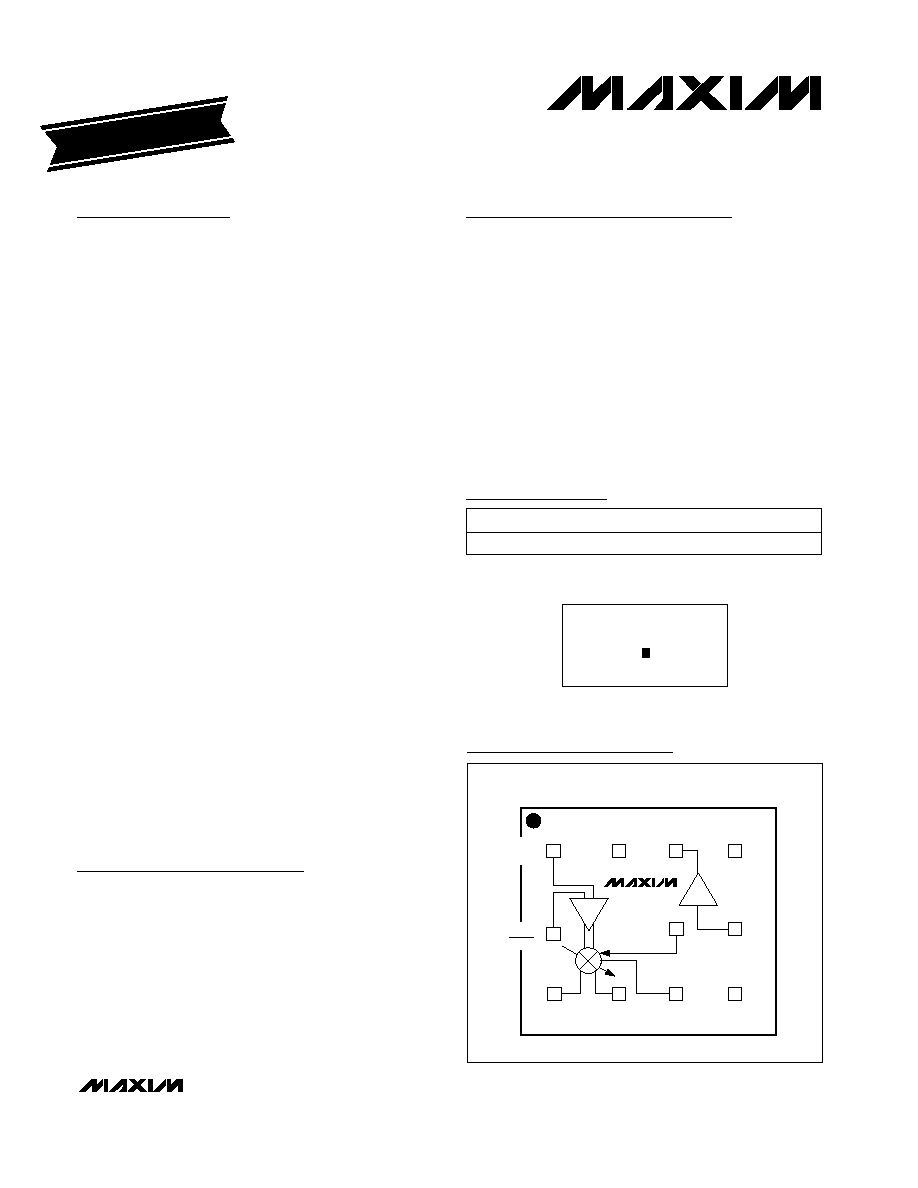
LO+ /
LO_EN
A1
B1
C1
C2
A2
C3
A3
B3
B4
C4
A4
LO-/
SHDN
PA
DRVR
IF
IN-
IF
IN+
RF
OUT
GND
DRIN
GC
V
CC
DROUT
GND
TOP VIEW
MAX2383
Block Diagram
Ordering Information
19-2108; Rev 1; 8/03
For pricing, delivery, and ordering information, please contact Maxim/Dallas Direct! at
1-888-629-4642, or visit Maxim's website at www.maxim-ic.com.
EVALUATION KIT
AVAILABLE
PART
TEMP RANGE
PIN-PACKAGE
MAX2383EBC-T
-40°C to +85°C
3 x 4 UCSP
Pin Configuration appears at end of data sheet.
Typical Operating Circuit appears at end of data sheet.
UCSP is a trademark of Maxim Integrated Products, Inc.

MAX2383
W-CDMA Upconverter and PA Driver
with Power Control
2
_______________________________________________________________________________________
ABSOLUTE MAXIMUM RATINGS
DC ELECTRICAL CHARACTERISTICS
(V
CC
= +2.7V to +3.0V, SHDN = +1.5V, T
A
= -40°C to +85°C. Typical values are at V
CC
= +2.85V, T
A
= +25°C, unless otherwise
noted.)
Stresses beyond those listed under "Absolute Maximum Ratings" may cause permanent damage to the device. These are stress ratings only, and functional
operation of the device at these or any other conditions beyond those indicated in the operational sections of the specifications is not implied. Exposure to
absolute maximum rating conditions for extended periods may affect device reliability.
V
CC
, RF
OUT
to GND ..............................................-0.3V to +6.0V
AC Signals ................................................................+1.0V Peak
SHDN, LO_EN, V
GC
to GND ......................-0.3V to (V
CC
+ 0.3V)
Digital Input Current ....................................................... ±10mA
Continuous Power Dissipation (T
A
= +70°C)
12-Pin UCSP (derate 80mW/°C above +70°C) ........ 628mW
Operating Temperature Range ..........................-40°C to +85°C
Junction Temperature .....................................................+150°C
Storage Temperature Range ............................-65°C to +160°C
Lead Temperature (Bump Reflow) ..................................+235°C
PARAMETER
SYMBOL
CONDITIONS
MIN
TYP
MAX
UNITS
Supply Voltage
V
CC
2.7
2.85
3.0
V
P
DROUT
= +6dBm, V
GC
= 2.0V
34
44
Operating Supply Current
I
CC
P
IF
-35dBm, V
GC
= 1.4V
12
20
mA
Shutdown Supply Current
I
CC
SHDN = 0.5V, LO_EN = 0.5V, V
GC
= 0.5V
0.5
10
µA
LO Buffer Current
I
CC
SHDN = 0.5V, LO_EN = 1.5V, V
GC
= 2V
6
8
mA
Digital Input Logic High
V
IH
1.5
V
CC
V
Digital Input Logic Low
V
IL
0
0.5
V
Input Logic High Current
I
IH
1
µA
Input Logic Low Current
I
IL
-1
µA
Recommended Gain-Control
Voltage
V
GC
0.5
2.0
V
Gain-Control Input Bias Current
I
GC
0.5V
V
GC
2.0V
-5
5
µA
AC ELECTRICAL CHARACTERISTICS
(MAX2383 EV Kit; V
CC
= +2.7V to +3.0V; SHDN = LO_EN = +1.5V; IF source impedance = 400
(differential), IF input level =
-16dBm (differential); LO input level = -10dBm, differential LO drive from 150
source impedance; mixer upconverter and PA driver
are cascaded directly through an interstage matching network; DROUT drives a 50
load impedance; V
GC
= 2.0V; f
IF
= 380MHz,
f
RF
= 1920MHz to 1980MHz, f
LO
= 2300MHz to 2360MHz; T
A
= -40°C to +85°C. Typical values are at V
CC
= +2.85V, T
A
= +25°C,
unless otherwise noted.) (Note 1)
PARAMETER
SYMBOL
CONDITIONS
MIN
TYP
MAX
UNITS
CASCADED PERFORMANCE (measured from IF input to DROUT (PA driver output))
IF Frequency
f
IF
(Note 2)
200600
MHz
RF Frequency Range
f
RF
(Note 2)
1920
1980
MHz
LO Frequency Range
f
LO
High-side LO case (Note 2)
22702580
MHz
3
limit
4.4
+6
Output Power (meets ACPR
specifications)
P
DROUT
V
GC
= 2.0V
6
limit
3.8
+6
dBm
Power Gain
G
P
V
GC
= 2.0V
17
19.5
dB
CAUTION! ESD SENSITIVE DEVICE
MAX2383
W-CDMA Upconverter and PA Driver
with Power Control
_______________________________________________________________________________________
3
AC ELECTRICAL CHARACTERISTICS (continued)
(MAX2383 EV Kit; V
CC
= +2.7V to +3.0V; SHDN = LO_EN = +1.5V; IF source impedance = 400
(differential), IF input level =
-16dBm (differential); LO input level = -10dBm, differential LO drive from 150
source impedance; mixer upconverter and PA driver
are cascaded directly through an interstage matching network; DROUT drives a 50
load impedance; V
GC
= 2.0V; f
IF
= 380MHz,
f
RF
= 1920MHz to 1980MHz, f
LO
= 2300MHz to 2360MHz; T
A
= -40°C to +85°C. Typical values are at V
CC
= +2.85V, T
A
= +25°C,
unless otherwise noted.) (Note 1)
PARAMETER
SYMBOL
CONDITIONS
MIN
TYP
MAX
UNITS
Gain-Control Range
V
GC
= 0.5V to 2.0V, P
IF
-35dBm
25
35
dB
Adjacent Channel Power Ratio
ACPR1
V
GC
= 2.0V (5MHz offset / 3.84MHz BW)
-46
dBc
Alternate Channel Power Ratio
ACPR2
V
GC
= 2.0V (10MHz offset / 3.84MHz BW)
-56
dBc
Out-of-Band Noise Power in
RX Band
V
GC
= 2.0V, P
DROUT
= +6dBm
(TX: 1980MHz; RX: 2110MHz)
-144
-140
dBm/
Hz
TX In-Band Noise Power
V
GC
= 2.0V, P
DROUT
= +6dBm
-139
-135
dBm/
Hz
TX In-Band Noise Power
V
GC
= 0.5V, P
DROUT
= -35dBm
-147
dBm/
Hz
Recommended LO Input Level
P
LO
Differential
-13
-10
-7
dBm
Note 1: Minimum and maximum values are guaranteed by design and characterization over temperature and supply voltages.
Note 2: Operation outside this frequency range is possible, but has not been verified.
Typical Operating Characteristics
(MAX2383 EV Kit; V
CC
= +2.85V; SHDN = LO_EN = V
CC
, V
GC
= 2.0V; IF source impedance = 400
(differential), IF input level =
-16dBm (differential); LO input level = -10dBm, differential LO drive from 150
source impedance; mixer upconverter and PA driver
are cascaded through an interstage matching network; DROUT drives a 50
load impedance; f
IF
= 380MHz, f
RF
= 1950 MHz, f
LO
=
2330MHz; T
A
= +25°C.)
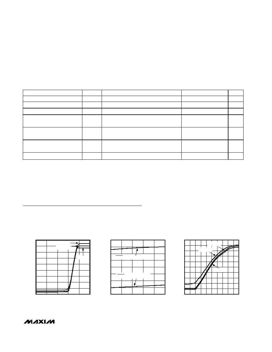
10
16
13
25
22
19
34
31
28
37
0
1.0
0.5
1.5
2.0
2.5
TOTAL SUPPLY CURRENT
vs. GAIN-CONTROL VOLTAGE
MAX2383 toc01
V
GC
(V)
TOTAL SUPPLY CURRENT (mA)
T
A
= +85
°C
T
A
= +25
°C
T
A
= -40
°C
0
5
10
15
20
25
30
35
40
-40
-15
10
35
60
85
TOTAL SUPPLY CURRENT
vs. TEMPERATURE
MAX2383 toc02
TEMPERATURE (
°C)
TOTAL SUPPLY CURRENT (mA)
SHDN = HIGH, LO_EN = HIGH
SHDN = LOW, LO_EN = HIGH
-25
-15
-20
-5
-10
5
0
10
20
15
25
0
0.4 0.6 0.8
0.2
1.0 1.2 1.4
1.8
1.6
2.0
CONVERSION POWER GAIN
vs. GAIN-CONTROL VOLTAGE
MAX2383 toc03
V
GC
(V)
CONVERSION POWER GAIN (dB)
T
A
= -40
°C
T
A
= +85
°C
T
A
= +25
°C

MAX2383
W-CDMA Upconverter and PA Driver
with Power Control
4
_______________________________________________________________________________________
18.0
19.0
18.5
20.0
19.5
20.5
21.0
CONVERSION POWER GAIN
vs. RF FREQUENCY
MAX2383 toc04
RF FREQUENCY (MHz)
CONVERSION POWER GAIN (dB)
1920
1940
1950
1930
1960
1970
1980
18.0
19.0
18.5
20.0
19.5
20.5
21.0
CONVERSION POWER GAIN
vs. LO INPUT LEVEL
MAX2383 toc05
P
LOIN
(dBm)
CONVERSION POWER GAIN (dB)
-13
-11
-10
-12
-9
-8
-7
4.0
5.0
4.5
6.0
5.5
6.5
7.0
-40
85
P
DROUT
vs. TEMPERATURE
MAX2383 toc06
TEMPERATURE (
°C)
P
DROUT
(dBm)
10
-15
35
60
ACPR = -46dBc
ACPR = -49dBc
Typical Operating Characteristics (continued)
(MAX2383 EV Kit; V
CC
= +2.85V; SHDN = LO_EN = V
CC
, V
GC
= 2.0V; IF source impedance = 400
(differential), IF input level =
-16dBm (differential); LO input level = -10dBm, differential LO drive from 150
source impedance; mixer upconverter and PA driver
are cascaded through an interstage matching network; DROUT drives a 50
load impedance; f
IF
= 380MHz, f
RF
= 1950 MHz, f
LO
=
2330MHz; T
A
= +25°C.)
-50
-40
-45
-30
-35
-25
-20
0.5
1.0
1.5
2.0
LO LEAKAGE vs. GAIN-CONTROL VOLTAGE
MAX2383 toc10
V
GC
(V)
LO LEAKAGE (dBm)
P
LO
= -7dBm
P
LO
= -10dBm
-36
-34
-32
-30
-28
-26
-24
-22
-20
1920
1940
1930
1950
1960
1970
1980
IMAGE SUPPRESSION vs. RF FREQUENCY
MAX2383 toc11
RF FREQUENCY (MHz)
IMAGE SUPPRESSION (dBc)
-75
-65
-70
-50
-55
-60
-35
-40
-45
-5
1
3
-3
-1
5
7
9
11
ACPR1 AND ACPR2 vs. P
DROUT
MAX2383 toc07
P
DROUT
(dBm)
ACPR AND ACPR2 (dBc)
-30
ACPR1 AT V
GC
= 1.5V
ACPR1 AT V
GC
= 1.7V
ACPR1 AT V
GC
= 2V
ACPR2 AT V
GC
= 1.7V
ACPR2 AT V
GC
= 2V
-150
-148
-149
-146
-147
-145
-144
-40
85
RX BAND NOISE POWER vs. TEMPERATURE
MAX2383 toc08
TEMPERATURE (
°C)
NOISE POWER (dBm/Hz)
10
-15
35
60
TX: 1980MHz,
NOISE MEASURED AT 2110MHz
P
DROUT
= +6dBm
-150
-146
-148
-142
-144
-138
-140
-136
INBAND NOISE POWER vs.
GAIN-CONTROL VOLTAGE
MAX2383 toc09
V
GC
(V)
NOISE POWER (dBm/Hz)
0
0.5
1.0
1.5
2.0
TX : 1980MHz,
NOISE MEASURED AT 1960MHz
-20
-16
-18
-12
-14
-10
-8
OUTPUT RETURN LOSS vs. RF FREQUENCY
MAX2383 toc12
RF FREQUENCY (MHz)
OUTPUT RETURN LOSS (dB)
1920
1940
1950
1930
1960
1970
1980
V
GC
= 2V
V
GC
= 1.7V
V
GC
= 1.4V
MAX2383
W-CDMA Upconverter and PA Driver
with Power Control
_______________________________________________________________________________________
5
Detailed Description
Variable-Gain Mixer
The MAX2383 contains a double-balanced Gilbert cell
mixer merged with a gain-control circuit, followed by a
mixer buffer. The mixer is driven differentially at its IF
ports. The LO input for the mixer is conditioned through
a low-noise, inductively loaded buffer. The mixer differ-
ential output is driven through an on-chip balun into a
single-ended common emitter amplifier, which drives
the output pin (RF
OUT
). The mixer buffer is a single-
ended in/out common emitter stage with inductive
degeneration and an external inductive load.
Additionally, these circuits are biased from "VCS" gen-
erators, designed to produce a low-noise constant
degeneration voltage at the user's current source.
These bias circuits also provide the control required to
selectively power-down the circuit and also provide for
gain control and current throttle-back.
PA Driver
The PA buffer is a single-ended in/out common emitter
stage with inductive degeneration and an external
inductive load.
Applications Information
LO Buffer Inputs
The external LO is interfaced either differentially or sin-
gle-ended to the differential LO buffer. Those two pins
also function as the control inputs for the device.
Hence, they are DC-coupled to the chip-control circuit-
ry, and AC-coupled to the LO port. SHDN and LO_EN
turn off the whole IC when both pins are pulled LOW.
LO_EN helps reduce VCO pulling in gated-transmission
mode by providing means to keep the LO buffer on
while the upconverter and driver turn on and off. To
avoid loading of the LO buffer, connect a 10k
isolation
resistor between the LO_EN/LO+ pin and the LO_EN
logic input, and a 10k
isolation resistor between the
SHDN/LO- pin and the SHDN logic input.
Differential IF Inputs
The MAX2383 has a differential IF input port for inter-
facing to differential IF filters. The IF pins should be AC-
coupled to the IF ports. The typical IF frequency is
380MHz, but the device can operate from 200MHz to
600MHz. The differential impedance between the two IF
inputs is approximately 400
in parallel with 1.0pF.
Interstage Matching
The mixer buffer drives the following PA driver through
an interstage matching network connected between the
mixer's RF
OUT
pin and the PA driver's input pin (DRIN).
This off-chip matching network, which consists of two
series inductors and a parallel capacitor, is designed to
achieve better than 25dBc image suppression with no
current consumption penalty. The quality factor of this
off-chip resonant circuit determines the image suppres-
sion level and usable bandwidth from the point of view
of passband gain flatness.
PA Driver Output
The PA driver output, DROUT, is an open-collector out-
put that requires an external inductor to V
CC
for proper
biasing. The output matching components are chosen
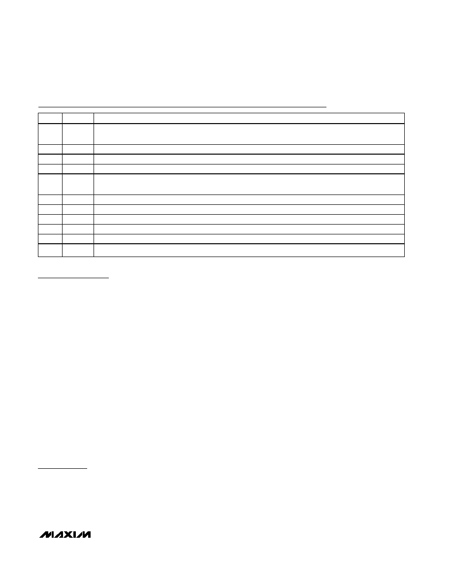
PIN
NAME
FUNCTION
A1+
LO_EN
/LO+
LO Buffer Enable Pin. When LOW, the LO buffer shuts off. Also noninverting input for LO port. It can be AC-
coupled to GND, when the LO is driven single-ended.
A2
V
CC
Power-Supply Pin. Bypass with a 330pF capacitor to GND as close to the pin as possible.
A3
DROUT
PA Driver Output Pin. Externally matched to 50
.
A4
GND
Ground Reference for RF
B1
SHDN/
LO-
Shutdown Pin. When LOW, the entire part shuts off, except for LO buffer. Also inverting input for LO port. It
can be AC-coupled to GND, when the LO is driven single-ended.
B3
GC
Power Control Input Pin (0.5V to 2.0V for control voltage)
B4
DRIN
PA Driver Input Pin (interstage node). Can be externally matched to 50
.
C1
IF
IN-
Inverting IF Input (400
differential nominal impedance between IF
IN+
and IF
IN-
)
C2
IF
IN+
Noninverting IF Input (400
differential nominal impedance between IF
IN+
and IF
IN-
)
C3
RF
OUT
Upconverter Output Port (interstage node). Can be externally matched to 50
.
C4
GND
Ground Reference for RF
Pin Description