MAX2369
Complete Dual-Band
Quadrature Transmitter
________________________________________________________________ Maxim Integrated Products
1
REF
N.C.
N.C.
N.C.
N.C.
TANK+
TANK-
IFLO
V
CC
SHDN
I-
I+
RFL
RFH
LOCK
V
CC
V
CC
V
CC
TXGATE
IFIN+
IFIN-
N.C.
N.C.
R
BIAS
1
2
3
4
5
6
7
8
9
10
11
12
13
14
15
16
17
18
19
20
21
22
23
24
48
47
46
45
44
43
42
41
40
39
38
37
36
35
34
33
32
31
30
29
28
27
26
25
CLK
DI
CS
V
CC
V
CC
IFOUT+
IFOUT-
V
GC
V
CC
V
CC
Q+
Q-
GND
GND
GND
GND
LOL
LOH
N.C.
V
CC
GND
V
CC
IFCP
V
CC
MAX2369
+45
-45
90
0
0
90
/2
IFPLL
/2
19-1924; Rev 1; 10/01
General Description
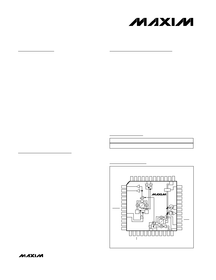
The MAX2369 is a dual-band, triple-mode complete
transmitter for cellular phones. The device takes a differ-
ential I/Q baseband input and mixes it up to IF through a
quadrature modulator and IF variable-gain amplifier
(VGA). The signal is then routed to an external bandpass
filter and upconverted to RF through an SSB mixer and
RF VGA. The signal is further amplified with an on-board
PA driver.
The MAX2369 is designed for dual-band operation and
supports TDMA for the PCS band as well as TDMA and
AMPS for the cellular band. The desired mode of
operation is selected by loading data on the SPITM/
MICROWIRETM-compatible 3-wire serial bus. The
MAX2369 then routes the signals to the appropriate ports
depending on which band is selected. The MAX2369
includes two RF LO input ports and two PA driver ports,
eliminating the need for external switching circuitry.
The MAX2369 takes advantage of the serial bus to set
modes such as charge-pump current, high or low side-
band injection, and IF/RF gain balancing. It is packaged
in a small (7mm
7mm) 48-pin QFN package with
exposed paddle.
Applications
Dual-Band TDMA/Amps Handsets
GAIT Handsets
Triple-Mode, Dual-Mode, or Single-Mode
Mobile Phones
Satellite Phones
Wireless Data Links (WAN/LAN)
Wireless Local Area Networks (LANs)
High-Speed Data Modems
High-Speed Digital Cordless Phones
Wireless Local Loop (WLL)
Features
o Dual-Band, Triple-Mode Operation
o +7dBm Output Power with -34dBc ACPR
(NADC Modulation)
o 100dB Power Control Range
o Supply Current Drops as Output Power Is Reduced
o On-Chip IF VCO and IF PLL
o QSPI/SPI/MICROWIRE-Compatible 3-Wire Bus
o Digitally Controlled Operational Modes
o +2.7V to +5.5V Operation
o Single Sideband Upconverter Eliminates SAW
Filters
o Power Control Distributed at IF and RF for
Optimum Dynamic Range
SPI and QSPI are trademarks of Motorola, Inc.
MICROWIRE is a trademark of National Semiconductor Corp.
Pin Configuration appears at end of data sheet.
Selector Guide appears at end of data sheet.
Functional Diagram
*Exposed paddle
For price, delivery, and to place orders, please contact Maxim Distribution at 1-888-629-4642,
or visit Maxim's website at www.maxim-ic.com.
Ordering Information
PART
TEMP. RANGE
PIN-PACKAGE
MAX2369EGM
-40
°C to +85°C
48 QFN-EP*
MAX2369
Complete Dual-Band
Quadrature Transmitter
2
_______________________________________________________________________________________
ABSOLUTE MAXIMUM RATINGS
DC ELECTRICAL CHARACTERISTICS
(MAX2369 Test Fixture: V
CC
= V
BATT
= +2.75V, SHDN = TXGATE = +2.0V, VGC = +2.5V, R
BIAS
= 16k
, T
A
= -40°C to +85°C,
unless otherwise noted. Typical values are at T
A
= +25°C, and operating modes are defined in Table 6.)
Stresses beyond those listed under "Absolute Maximum Ratings" may cause permanent damage to the device. These are stress ratings only, and functional
operation of the device at these or any other conditions beyond those indicated in the operational sections of the specifications is not implied. Exposure to
absolute maximum rating conditions for extended periods may affect device reliability.
V
CC
to GND ...........................................................-0.3V to +3.6V
RFL, RFH.............................................................................+5.5V
DI, CLK, CS, VGC, SHDN, TXGATE,
LOCK.....................................................-0.3V to (V
CC
+ 0.3V)
AC Input Pins (IFIN, Q, I, TANK, REF,
LOL, LOH) ...............................................................1.0V peak
Digital Input Current (SHDN, TXGATE,
CLK, DI, CS) ................................................................±10mA
Continuous Power Dissipation (T
A
= +70°C)
48-Pin QFN-EP (derate 27mW/°C above +70°C) ..............2.5W
Operating Temperature Range ...........................-40°C to +85°C
Junction Temperature ......................................................+150°C
Storage Temperature Range .............................-65°C to +160°C
Lead Temperature (soldering, 10s) .................................+300°C
PARAMETER
CONDITIONS
MIN
TYP
MAX
UNITS
Operating Supply Voltage
2.7
3.0
V
VGC = 0.5V
80
106
VGC = 2.0V
85
112
PCS mode
VGC = 2.5V
120
150
VGC = 0.5V
82
107
VGC = 2.0V
87
113
Cellular
digital mode
VGC = 2.5V
123
155
VGC = 0.5V
77
101
VGC = 2.0V
80
105
FM mode
VGC = 2.5V
105
133
mA
(Note 1)
Addition for IFLO buffer
6.5
11
TXGATE = 0.6V
16
25
Operating Supply Current
SHDN = 0.6V, sleep mode
0.5
20
µA
Logic High
2.0
V
Logic Low
0.6
V
Logic Input Current
-5
+5
µA
VGC Input Current
-12
+12
µA
VGC Input Resistance During Shutdown
SHDN = 0.6V
200
280
k
Lock Indicator High
50k
pullup load
V
CC
- 0.4
V
Lock Indicator Low
50k
pullup load
0.4
V
MAX2369
Complete Dual-Band
Quadrature Transmitter
_______________________________________________________________________________________
3
AC ELECTRICAL CHARACTERISTICS
(MAX2369 Evaluation Kit: 50
system, operating modes as defined in Table 6, input voltage at I and Q = 200mV
RMS
differential,
common mode = V
CC
/2, 300kHz quadrature CW tones, IF synthesizer locked with passive lead-lag second-order loop filter, REF =
200mVp-p at 19.44MHz, V
CC
= SHDN = CS = TXGATE = +2.75V, V
BAT
= +2.75V, IF output load = 400
, LOH, LOL input power =
-7dBm, f
LOL
= 1017.26MHz, f
LOH
= 2061.26MHz, IFIN = 125mV
RMS
at 181.26MHz, IS-136 TDMA modulation, f
RFH
= 1880MHz, f
RFL
= 836MHz, T
A
= +25°C, unless otherwise noted.)
PARAMETER
CONDITIONS
MIN
TYP
MAX
UNITS
MODULATOR, QUADRATURE MODES (Digital Cellular, Digital PCS, FM IQ)
IF Frequency Range
120235
MHz
I/Q Common-Mode Input
Voltage
V
CC
= 2.7V to 3.0V (Notes 2, 3, 4)
1.35
V
CC
/ 2
V
CC
1.25
V
IF Gain Control Range
VGC = 0.5V to 2.5V, IFG = 100
85
dB
IF Output Power, Digital Mode
VGC = 2.5V, IFG = 100
-10
dBm
Gain Variation Over Temperature
Relative to +25
°C, T
A
= -40
°C to +85°C (Note 4)
±0.8
dB
RX Band Noise Power
VGC = 2.5V, IFG = 100, F
IF
= 181.26MHz, noise
measured at F
IF
± 20MHz
-145
dBm/Hz
Carrier Suppression
VGC = 2.5V, IFG = 100
30
49
dB
Sideband Suppression
VGC = 2.5V, IFG = 100
30
38
dB
MODULATOR, FM MODE
IF Gain Control Range
VGC = 0.5V to 2.5V, IFG = 100
85
dB
VGC = 2.5V, IFG = 111, I/Q modulation
-8.5
Output Power
VGC = 2.5V, IFG = 111, direct VCO modulation
-5.5
dBm
UPCONVERTER AND PREDRIVER
IF Frequency Range
120235
MHz
Low-Band Frequency Range
RFL port
8001000
MHz
High-Band Frequency Range
RFH port
17002000
MHz
LOL Frequency Range
8001150
MHz
LOH Frequency Range
14002300
MHz
VGC = 2.5V, NADC modulation, ACPR < -32dBc/
-55dBc at +30kHz/+60kHz offset
5.8
7
Output Power, RFL (Note 4)
VGC = 2.5V, FM mode
9
12
dBm
Output Power, RFH (Note 4)
VGC = 2.6V, NADC modulation, ACPR = -32dB/
-55dBc at +30kHz/+60kHz offset
4
6.6
dBm
Power-Control Range
VGC = 0.5V to 2.5V
30
dB
Gain Variation Over Temperature
Relative to +25
°C, T
A
= -40
°C to +85°C (Note 4)
±3
dB
RFL
-25
RF Image Rejection (Note 4)
RFH
-24
dBc
RFL, VGC = 2.5V
-22
LO Leakage (Note 4)
RFH, VGC = 2.6V
-24
dBm
RFL, VGC = 2.5V
-133
RX Band Noise Power
RFH, VGC = 2.6V
-134
dBm/
Hz

MAX2369
Complete Dual-Band
Quadrature Transmitter
4
_______________________________________________________________________________________
AC ELECTRICAL CHARACTERISTICS (continued)
(MAX2369 Evaluation Kit: 50
system, operating modes as defined in Table 6, input voltage at I and Q = 200mV
RMS
differential,
common mode = V
CC
/2, 300kHz quadrature CW tones, IF synthesizer locked with passive lead-lag second-order loop filter, REF =
200mVp-p at 19.44MHz, V
CC
= SHDN = CS = TXGATE = +2.75V, V
BAT
= +2.75V, IF output load = 400
, LOH, LOL input power =
-7dBm, f
LOL
= 1017.26MHz, f
LOH
= 2061.26MHz, IFIN = 125mV
RMS
at 181.26MHz, IS-136 TDMA modulation, f
RFH
= 1880MHz, f
RFL
= 836MHz, T
A
= +25°C, unless otherwise noted.)
Note 1: See Table 6 for register settings.
Note 2: ACPR is met over the specified V
CM
range.
Note 3: V
CM
must be supplied by the I/Q baseband source with ±6µA capability.
Note 4: Guaranteed by design and characterization.
Note 5: When enabled, turbolock is active during acquisition and injects boost current in addition to the normal charge-pump current.
Note 6: Charge Pump Compliance range is 0.5V to V
CC
- 0.5V.
PARAMETER
CONDITIONS
MIN
TYP
MAX
UNITS
IF_PLL
Reference Frequency
5
30
MHz
Frequency Reference Signal
Level
0.1
0.6
Vp-p
IF Main Divide Ratio
256
16384
IF Reference Signal Ratio
2
2048
VCO Operating Range
240470
MHz
IF LO Output Power
BUF_EN = 1
-6
dBm
ICP = 00
148
200
260
ICP = 01
185
260
345
ICP = 10
295
400
515
Charge-Pump Source/Sink
Current
ICP = 11
385
530
700
µA
Turbolock Boost Current
(Note 5)
385
530
700
µA
Charge-Pump Source/Sink
Matching
Locked, all values of ICP, over specified compliance
range (Note 6)
5
%
Charge-Pump High-Z Leakage
Over specified compliance range (Note 6)
10
nA

MAX2369
Complete Dual-Band
Quadrature Transmitter
_______________________________________________________________________________________
5
Typical Operating Characteristics
(MAX2369EVKIT, V
CC
= +2.8V, V
BAT
= 3.0V, T
A
= +25°C, unless otherwise noted.)
-10
-6
-8
-2
-4
2
0
4
8
6
10
0
200 300 400
100
500 600 700
900
800
1000
IF P
LL
SETTLING TIME
TIME (µs)
FREQUENCY DEVIATION (kHz)
MAX2369 toc01
f
IF
= 181.26MHz
TANK 1/S11 vs. FREQUENCY
MAX2369 toc02
4
5
1
2
3
z
0
= 200
EQUIVALENT PARALLEL R-C
1: 200MHz, 1.76k
, 0.26pF
2: 260MHz, 1.66k
, 0.31pF
3: 330MHz, 1.58k
, 0.34pF
4: 780MHz, 1.21k
, 0.43pF
5: 1GHz, 0.94k
, 0.47pF
80
100
90
120
110
130
140
1.5
1.7 1.8 1.9
1.6
2.0 2.1 2.2 2.3 2.4 2.5 2.6
I
CC
vs. VGC INPUT
MAX2369 toc03
VGC (V)
I
CC
(mA)
CELLULAR
PCS
-30
-35
-40
-45
-50
-55
-60
-20
-25
-10
-15
-5
5
0
10
OUTPUT POWER vs. VGC INPUT
MAX2369 toc04
VGC (V)
OUTPUT POWER (dBm)
1.5
1.9
2.1
1.7
2.3
2.5
CELLULAR
PCS
-120
-80
-100
-40
-60
-20
0
0
1.0
1.5
0.5
2.0
2.5
3.0
IF OUTPUT POWER
vs. VGC INPUT AND IF DAC SETTING
MAX2369 toc05
VGC (V)
P
OUT
(dBm)
011
111
100
101
110
001
000
010
-110
-90
-100
-40
-50
-60
-70
-80
-30
-20
-10
0
1.0
0
1.5
0.5
2.0
2.5
3.0
IF OUTPUT POWER vs. VGC INPUT
MAX2369 toc06
VGC (V)
IF POWER
(dBm)
-40°C
+85°C
+25°C
-120
-80
-100
-40
-60
-20
0
0
1.0
1.5
0.5
2.0
2.5
3.0
IF OUTPUT POWER vs. VGC INPUT
MAX2369 toc07
VGC (V)
P
OUT
(dBm)
2.7V, 3.0V, 3.3V
-100
-80
-90
-60
-70
-40
-50
-30
-10
-20
0
181.21
181.23
181.25
181.27
181.29
181.31
SIDEBAND SUPPRESSION AND LO
FEEDTHROUGH (IFOUT)
MAX2369 toc08
FREQUENCY (MHz)
P
OUT
(dBm)
SIDEBAND
DESIRED
LO