
________________General Description
The MAX2323/MAX2325 are low-noise amplifier (LNA)
plus mixer ICs optimized for code-division multiple-access
(CDMA) applications in both cellular and PCS bands. The
MAX2323 addresses dual-band, triple-mode CDMA appli-
cations by providing switched signal paths for cellular FM,
cellular CDMA, and PCS CDMA. The MAX2325 is a cellu-
lar-band dual-mode version.
To optimize cellular-band dynamic range at minimum cur-
rent, the MAX2323/MAX2325 implement four LNA states:
high gain/high linearity, high gain/low linearity, midgain,
and low gain. In high-gain/high-linearity mode, the
adjustable high-intercept LNA minimizes desensitization in
the presence of a large interfering signal. For the other
gain states, the LNA current is reduced to improve stand-
by time.
The CDMA mixers are designed for high linearity, low
noise, and differential IF outputs, while the FM mixer is
designed for lower current and single-ended output. Each
band is implemented with a separate mixer to optimize
performance for the specific band.
The MAX2323/MAX2325 can also be used in TDMA,
EDGE, and W-CDMA phones.
________________________Applications
Dual-Band, Triple-Mode PCS/Cellular Phones
Dual-Mode Cellular Phones
____________________________Features
o 2.7V Operation
o Dual Band, Triple Mode
o Three LNA Gain Settings (Cellular)
o Two LNA Gain Settings (PCS)
o 18mA in Low-Gain Mode
19.5mA in Paging and Midgain Mode
26.5mA in High-Gain, High-Linearity Mode
16.5mA in FM Mode, High-Gain, Low-Linearity
Mode
o 2.5dB (typ) Cascade Noise Figure
o Adjustable LNA IIP3, +5dBm to +13dBm
o Ultra-Small 28-Pin Package (5mm x 5mm)
MAX2323/MAX2325
Triple/Dual-Mode
CDMA LNA/Mixers
________________________________________________________________ Maxim Integrated Products
1
19-1736; Rev 0; 7/00
For free samples and the latest literature, visit www.maxim-ic.com or phone 1-800-998-8800.
For small orders, phone 1-800-835-8769.
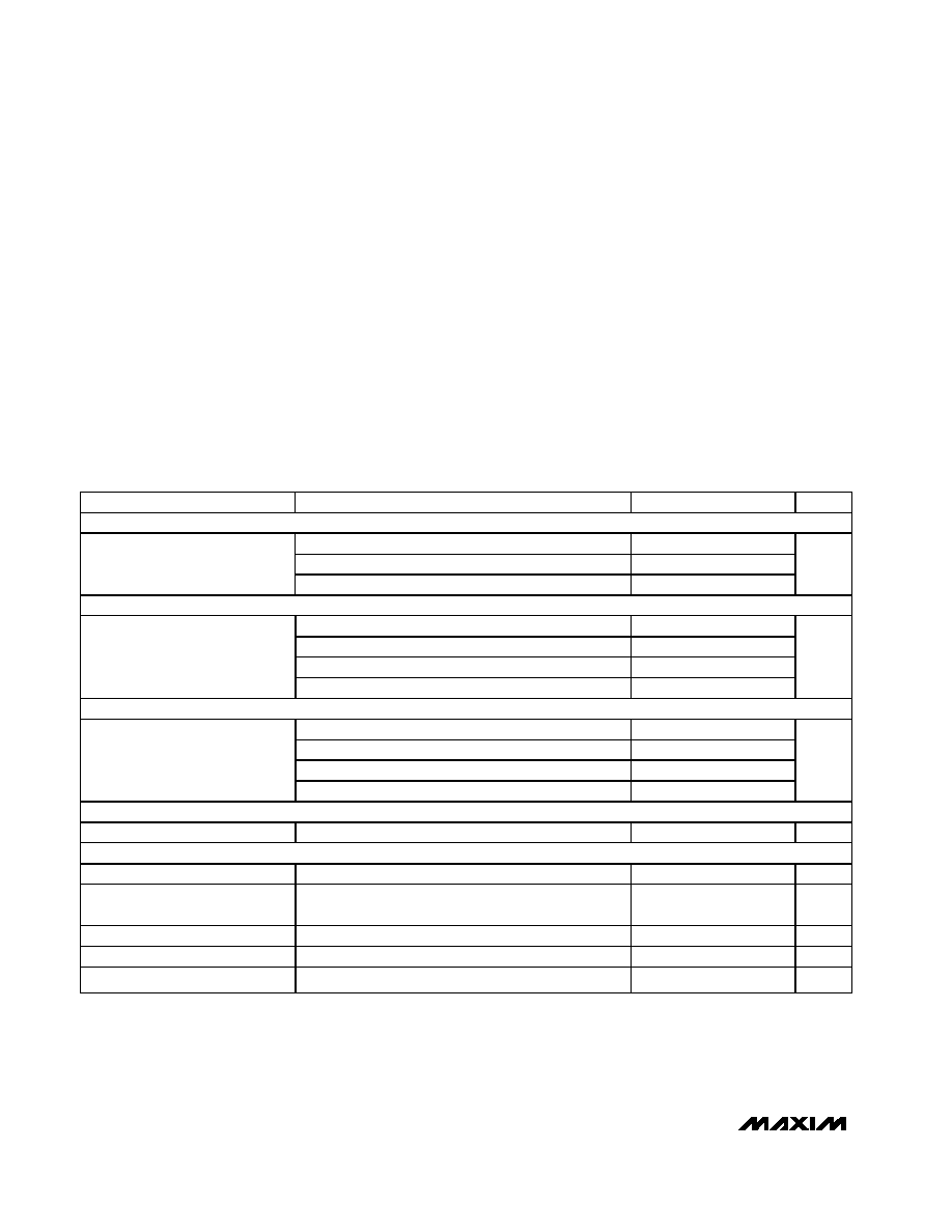
Pin Configuration/
Functional Diagram
Typical Application Circuits appear at end of data sheet.
MAX2323
25
26
27
28
22
23
24
8
9
10
11
12
13
14
15
16
17
18
19
20
21
1
2
3
4
5
6
7
MODE.
GND
LOLIN
LOHIN
GND
GND
GND
CMIXIN
CLNAOU
T
GND
PLNAOU
T
GND
GND
PMIXIN
GND
CLNAIN
SLEEP
G2
G1
PLNAIN
RLNA
CDMA-
GND
BAND
V
CC
FMOUT
CDMA+
RBIAS
QFN
TOP VIEW
PART
TEMP. RANGE
PIN- PACKAGE
MAX2323EGI
-40
�C to +85�C
28 QFN
MAX2325EGI
-40
�C to +85�C
28 QFN
MAX2323EVKIT
-40
�C to +85�C
28 QFN
Ordering Information
MAX2323/MAX2325
Triple/Dual-Mode
CDMA LNA/Mixers
2
_______________________________________________________________________________________
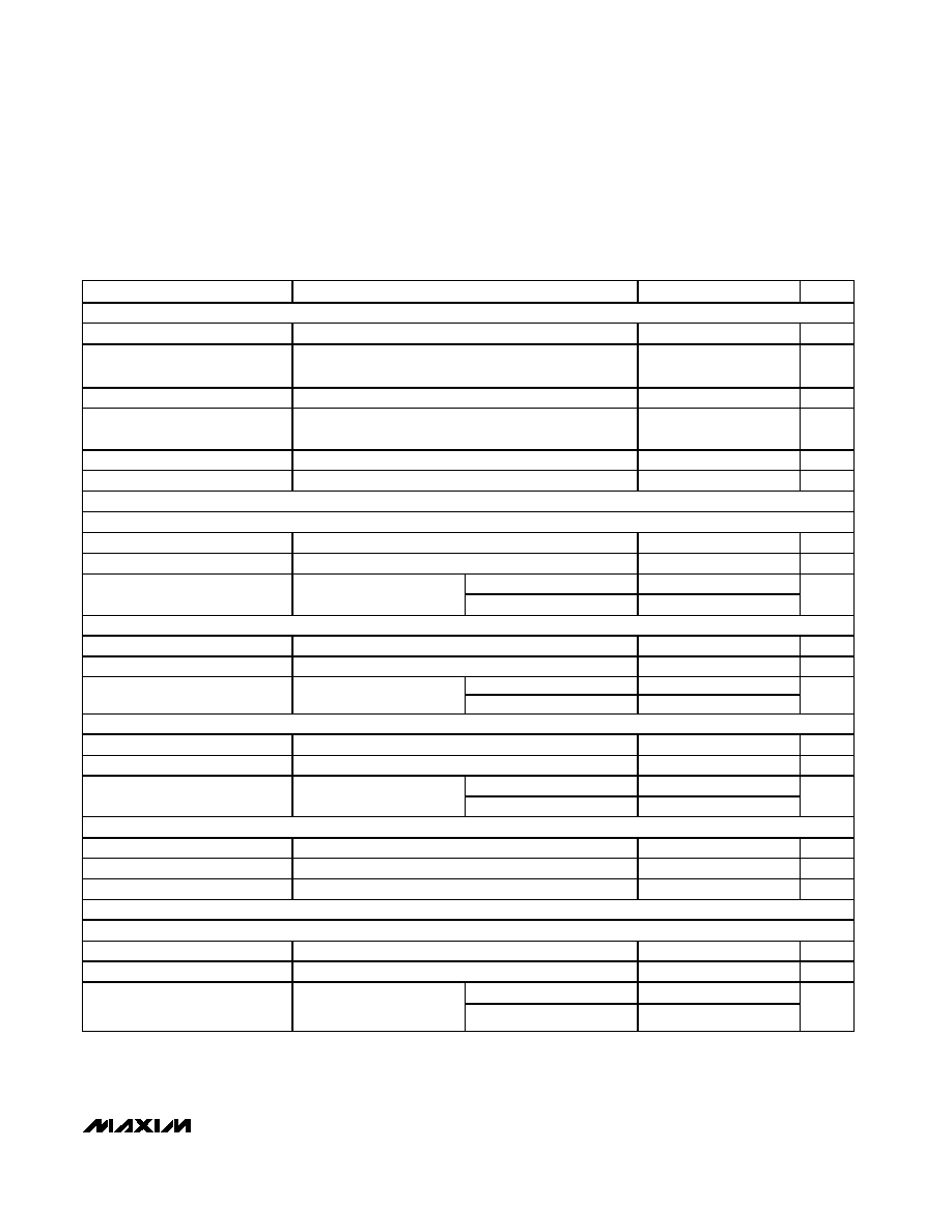
ABSOLUTE MAXIMUM RATINGS
DC ELECTRICAL CHARACTERISTICS
(V
CC
= +2.7V to +3.6V, R
RBIAS
= 20k
, R
RLNA
= 24k
, T
A
= -40�C to +85�C, no RF applied. Typical values are V
CC
= 2.75V and
T
A
= +25�C, unless otherwise noted.)
Stresses beyond those listed under "Absolute Maximum Ratings" may cause permanent damage to the device. These are stress ratings only, and functional
operation of the device at these or any other conditions beyond those indicated in the operational sections of the specifications is not implied. Exposure to
absolute maximum rating conditions for extended periods may affect device reliability.
V
CC
to GND ...............................................................0.3V, +4.3V
Digital Input Voltage to GND ......................-0.3V to (V
CC
+ 0.3V)
LNA Input Level .....................................................................1Vp
LO, Mixer Input Levels .....................................................+5dBm
Digital Input Current .........................................................�10mA
Continuous Power Dissipation (T
A
= +70�C)
28-Pin QFN (derate 28.5mW/�C
above T
A
= +70�C) ...................................................2000mW
Operating Temperature Range ...........................-40�C to +85�C
Junction Temperature ......................................................+150�C
Storage Temperature Range .............................-65�C to +150�C
Lead Temperature (soldering, 10s) ................................ +300�C
PARAMETER
CONDITIONS
MIN
TYP
MAX
UNITS
PCS CDMA MODE (MAX2323)
Midgain mode
20.5
24
High-gain, low-linearity idle mode
22
25.5
Operating Supply Current
High-gain, high-linearity mode
25.5
30
mA
CELLULAR CDMA MODE (MAX2323/MAX2325)
Low-gain mode
18.0
21.5
Midgain mode
19.5
23.5
High-gain, low-linearity idle mode
19.5
23.5
Operating Supply Current
High-gain, high-linearity mode
26.5
31.5
mA
FM MODE (MAX2323/MAX2325)
Low-gain mode
15
18
Midgain mode
16.5
20
High-gain, low-linearity mode
16.5
20
Operating Supply Current
High-gain, high-linearity mode
23.5
28
mA
SHUTDOWN MODE
Shutdown Supply Current
SLEEP = high
1
25
�A
ALL MODES
Digital Input Logic High
Except SLEEP input
2.0
V
SLEEP Input Logic High
V
CC
-
0.6
V
Digital Input Logic Low
0.6
V
Digital Input Current High
5
�A
Digital Input Current Low
-25
�A
MAX2323/MAX2325
Triple/Dual-Mode
CDMA LNA/Mixers
_______________________________________________________________________________________
3
AC ELECTRICAL CHARACTERISTICS
(MAX2323 EV kit, F
PLNAIN
= 1960MHz, F
CLNAIN
= 881MHz, F
IF
= 110MHz, high-side LO, 50
system, R
RBIAS
= 20k
,
R
RLNA
= 24k
. Typical values are V
CC
= 2.75V, T
A
= +25�C. LO input power = -7dBm, LOW = 0V, HIGH = V
CC
, unless otherwise
noted.) (Note 1)
PARAMETER
CONDITIONS
MIN
TYP
MAX
UNITS
OVERALL PERFORMANCE
Low-Band RF Frequency Range
(Note 2)
850
950
MHz
High-Band RF Frequency
Range
MAX2323 (Note 2)
1800
2200
MHz
Low-Band LO Frequency Range
(Note 2)
800
1150
MHz
High-Band LO Frequency
Range
MAX2323 (Note 2)
1600
2300
MHz
IF Frequency Range
(Note 2)
40
400
MHz
LO Input Level
100
input impedance
-7
-5
0
dBm
CELLULAR LNA PERFORMANCE (MAX2323/MAX2325)
CDMA AND FM HIGH-GAIN, HIGH-LINEARITY MODES
Gain
T
A
= T
MIN
to T
MAX
14.5
15.5
17
dB
Noise Figure
1.7
1.9
dB
T
A
= +25
�C
9
10.5
IIP3
T
A
= T
MIN
to T
MAX
7.5
dBm
CDMA HIGH-GAIN, LOW-LINEARITY PAGING MODE, AND FM HIGH-GAIN MODE
Gain
T
A
= T
MIN
to T
MAX
13
14.5
16
dB
LNA Noise Figure
1.7
1.9
dB
T
A
= +25
�C
2.5
5
LNA IIP3
(Note 3)
T
A
= T
MIN
to T
MAX
2.7
dBm
CDMA AND FM MIDGAIN MODES
Gain
T
A
= T
MIN
to T
MAX
4.5
6
8
dB
Noise Figure
3.3
3.5
dB
T
A
= +25
�C
8.5
10
IIP3
(Note 3)
T
A
= T
MIN
to T
MAX
5
dBm
CDMA AND FM LOW-GAIN MODES
Gain
T
A
= T
MIN
to T
MAX
-4.5
-3.5
-1.5
dB
Noise Figure
7.5
8.5
dB
IIP3
(Note 3)
13
17.5
dBm
PCS LNA PERFORMANCE (MAX2323)
CDMA HIGH-GAIN, HIGH-LINEARITY MODE
Gain
T
A
= T
MIN
to T
MAX
13.5
14.5
15.5
dB
Noise Figure
1.9
2.1
dB
T
A
= +25
�C
7
8
IIP3
(Note 3)
T
A
= T
MIN
to T
MAX
5.5
dBm
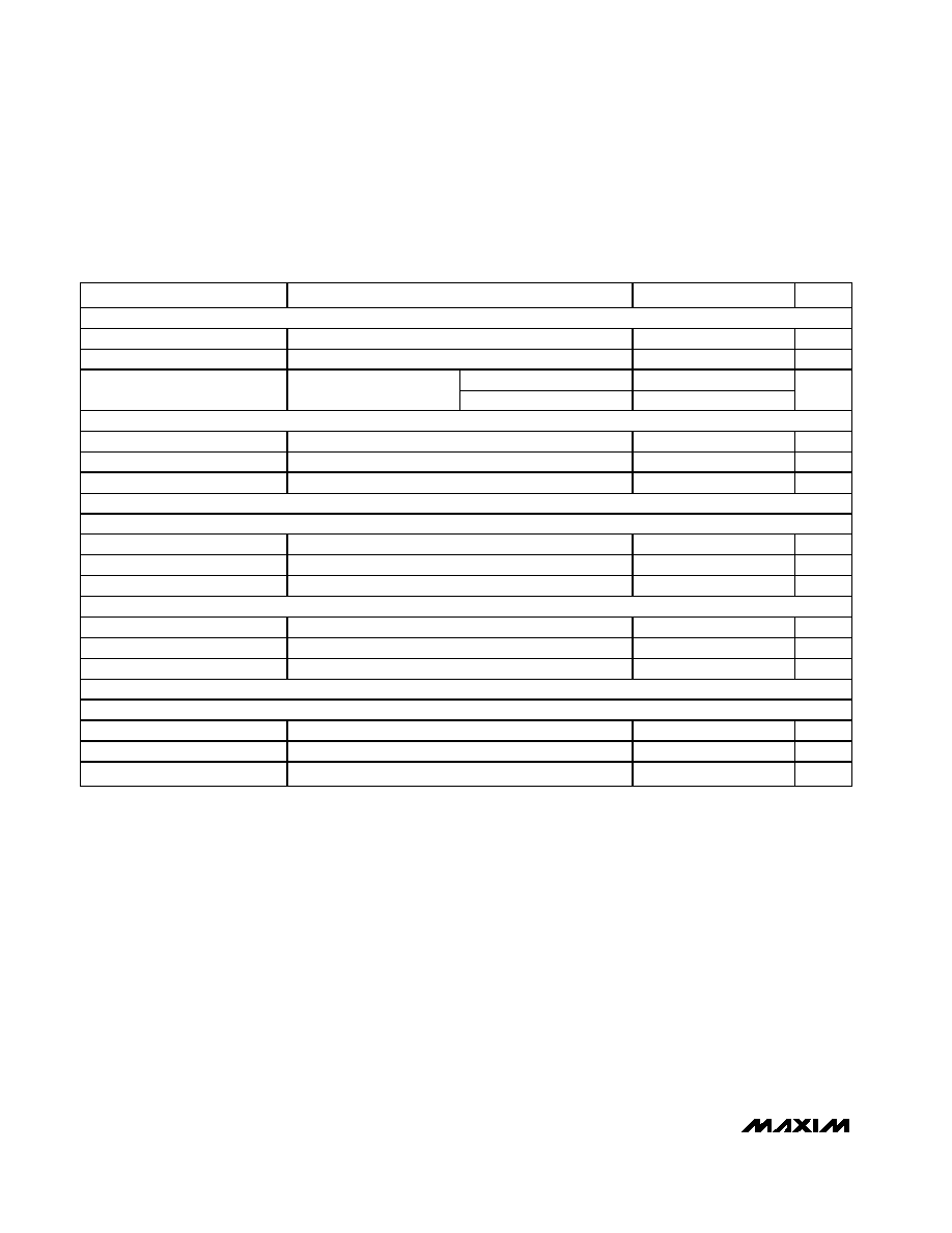
Note 1: Devices are production tested for functionality at frequencies stated; 30 units from 3 independent wafer lots, when one lot
was at the upper process extreme, one lot was nominal, and one lot was at the lower process extreme, were characterized.
The resulting standard deviation therefore includes process variations. Data sheet limits are �3
from the mean.
Note 2: Operation over this frequency range requires the ports to be rematched for the desired operating range. Performance at
various frequencies is indicated by the S-parameter data in Tables 3�7.
Note 3: Specifications are based on R
BIAS
= 20k
. I
CC
for all LNAs (except HGHL) and mixers are inversely proportional to R
RBIAS
.
IIP3 can be traded for I
CC
by selecting other values of R
RBIAS
.
MAX2323/MAX2325
Triple/Dual-Mode
CDMA LNA/Mixers
4
_______________________________________________________________________________________
AC ELECTRICAL CHARACTERISTICS (continued)
(MAX2323 EV kit, F
PLNAIN
= 1960MHz, F
CLNAIN
= 881MHz, F
IF
= 110MHz, high-side LO, 50
system, R
RBIAS
= 20k
,
R
RLNA
= 24k
. Typical values are V
CC
= 2.75V, T
A
= +25�C. LO input power = -7dBm, LOW = 0V, HIGH = V
CC
, unless otherwise
noted.) (Note 1)
PARAMETER
CONDITIONS
MIN
TYP
MAX
UNITS
CDMA HIGH-GAIN, LOW-LINEARITY PAGING MODE
Gain
T
A
= T
MIN
to T
MAX
12.5
14
14.5
dB
LNA Noise Figure
1.9
2.1
dB
T
A
= +25
�C
4.5
5.5
LNA IIP3
(Note 3)
T
A
= T
MIN
to T
MAX
3.0
dBm
CDMA MIDGAIN MODE
Gain
T
A
= T
MIN
to T
MAX
-2.0
-1.0
-0.5
dB
Noise Figure
5.6
6.0
dB
IIP3
(Note 3)
12
13.5
dBm
CELLULAR MIXER PERFORMANCE (MAX2323/MAX2325)
CDMA, ALL MODES
Gain
T
A
= T
MIN
to T
MAX
11.5
13
14.5
dB
Noise Figure
7.5
8.5
dB
IIP3
T
A
= T
MIN
to T
MAX
(Note 3)
3.5
4.8
dBm
FM MODE
Gain
T
A
= T
MIN
to T
MAX
8.5
10
11.5
dB
Noise Figure
10.5
11.5
dB
IIP3
T
A
= T
MIN
to T
MAX
(Note 3)
1.5
5
dBm
PCS MIXER PERFORMANCE (MAX2323)
CDMA HIGH-GAIN, HIGH-LINEARITY MODE
Gain
T
A
= T
MIN
to T
MAX
12
13.5
15.5
dB
Noise Figure
7.9
8.5
dB
IIP3
T
A
= T
MIN
to T
MAX
(Note 3)
1.5
4
dBm

MAX2323/MAX2325
Triple/Dual-Mode
CDMA LNA/Mixers
_______________________________________________________________________________________
5
Pin Description
PIN
MAX2323
MAX2325
NAME
FUNCTION
1
1
RLNA
L N A B i a s - S e t t i ng P i n . F o r no m i n a l b i a s , c o n n ec t a 24 k
r es i s t o r t o g r o u n d . T h i s
r e si s t o r v a l u e c a n b e a d j u st e d t o a l t e r t h e l i n e a r i t y o f t h e i np u t L N A i n hi g h - g ai n ,
h i g h - l i n ea r i t y C D M A m o d e s .
--
2, 10, 23
N.C.
No Connection. Leave this pin floating.
2
--
PLNAIN
High-Band RF Input Port. Blocking capacitor is required, which may be used as part of
the matching network.
3, 8, 11,
12, 13, 18,
24, 25, 27
3, 8, 11, 12,
13, 17, 18,
24, 25, 27
GND
Ground
4
4
CLNAIN
Low-Band RF Input Port. Blocking capacitor is required, which may be used as part of
the matching network.
5
5
SLEEP
Logic Input. High shuts off entire device.
6
6
G2
Logic Input. See Tables 1 and 2 for details.
7
7
G1
Logic Input. See Tables 1 and 2 for details.
9
9
LOLIN
Low-Frequency LO Input Port. Requires blocking capacitor, which may be used as
part of an optional matching network.
10
--
LOHIN
High-Frequency LO Input Port. Requires blocking capacitor, which may be used as
part of an optional matching network.
14
14
MODE
Logic Input. See Tables 1 and 2 for details.
15
15
FMOUT
FM IF Output Port. Requires a pull-up inductor and a DC blocking capacitor, which
may be used as part of the matching network.
16
16
V
CC
2.7V to 3.6V Supply Pin. Must be capacitively bypassed near the pin.
17
--
BAND
Logic Input. High selects high band (PCS). Low selects low band (cellular).
19, 20
19, 20
CDMA-,
CDMA+
Differential Output Port for CDMA Mode. Requires pull-up inductors and blocking
capacitors, which may be used as part of the matching network.
21
21
RBIAS
Bias Setting Pin. For nominal bias, connect a 20k
resistor to ground. This resistor
value can be adjusted to alter the linearity of the mixers in all modes and the LNA in all
modes except high gain and high linearity.
22
22
CMIXIN
Low-Band Mixer Input Port. Requires blocking capacitor, which may be used as part of
the matching network.
23
--
PMIXIN
High-Band Mixer Input Port. Requires blocking capacitor, which may be used as part
of the matching network.
26
--
PLNAOUT
High-Band LNA Output Port. This port requires an external pull-up inductor and series
capacitor as part of the matching network.
--
26
V
CC
2.7 to 3.6V Supply Pin. Bypassing is not necessary at this pin.