
General Description
The MAX2251 low-voltage linear power amplifier (PA) is
designed for TDMA/AMPS dual-mode phone applica-
tions. The device is packaged in an ultra-compact
(2.06mm
2.06mm) chip-scale package (CSP), and
delivers over +30dBm of linear power in TDMA opera-
tion. An on-chip shutdown feature reduces operating
current to 1µA (typ), eliminating the need for an external
supply switch.
The MAX2251 does not need an external reference volt-
age, and requires only a few external matching compo-
nents and no bias circuitry. Another feature of this
device is the use of external bias resistors, eliminating
wasted "safety-margin" current. This feature also allows
current throttleback at lower output power levels, there-
by maintaining the highest possible efficiency at all
power levels.
________________________Applications
Cellular-Band TDMA/AMPS Dual-Mode Phones
PA Modules
2-Way Pagers
Cordless Phones
Features
o Ultra-Compact 4
4 (2.06mm
2.06mm) CSP
o High Efficiency--41% at +30dBm P
OUT
(TDMA)
(typ)
o On-Chip Power Detector
o I
CC
< 1µA in Shutdown Mode
o +2.8V to +4.5V True Single-Supply Operation
o ±0.9dB Gain Variation from T
A
= -40°C to +85°C
o Current Adjustable with PDM or DAC Signal
o No External Logic Interface Circuitry Required
MAX2251
+2.8V, Single-Supply,
Cellular-Band Linear Power Amplifier
________________________________________________________________ Maxim Integrated Products
1
PIN A1
INDICATOR
POWER
DETECTOR
LOGIC AND
BIAS
A1
A2
GND
A3
GND
A4
GND
PD_OUT
B1
GND
B2
OUT
B3
OUT
B4
D1
V
CC
C2
GND
D2
IN
C3
V
CC
D3
SHDN
C4
GND
D4
MODE
BIAS1
C1
TOP VIEW
BIAS2
MAX2251
Pin Configuration
19-1773; Rev 2; 2/03
EVALUATION KIT
AVAILABLE
Ordering Information
PART
TEMP
RANGE
PIN-
PACKAGE
TOP MARK
MAX2251EBE - 40°C to + 85° C 4
× 4 U C S P
2251
EBE
_ _ _ (LOT #)
_ _ _ (D ATE CODE)
Typical Operating Circuit appears at end of data sheet.
For price, delivery, and to place orders, please contact Maxim Distribution at 1-888-629-4642,
or visit Maxim's website at www.maxim-ic.com.
MAX2251
+2.8V, Single-Supply,
Cellular-Band Linear Power Amplifier
2
_______________________________________________________________________________________
ABSOLUTE MAXIMUM RATINGS
Stresses beyond those listed under "Absolute Maximum Ratings" may cause permanent damage to the device. These are stress ratings only, and functional
operation of the device at these or any other conditions beyond those indicated in the operational sections of the specifications is not implied. Exposure to
absolute maximum rating conditions for extended periods may affect device reliability.
V
CC
to GND ..........................................................-0.3V to +4.5V
SHDN, MODE to GND ................................-0.3V to (V
CC
+ 0.3V)
BIAS_ to GND.............................................-0.3V to (V
CC
+ 0.3V)
RF Input Power ...............................................................+10dBm
Continuous Power Dissipation (T
A
= +70°C)
4
4 UCSP (derate 80mW/°C above +70°C) ....................4W
Operating Temperature Range ...........................-40°C to +85°C
Junction Temperature ......................................................+150°C
Thermal Resistance from Junction to Backside.................1°C/W
Thermal Resistance from Junction to Ambient
(using MAX2251 EV kit)...............................................40°C/W
Storage Temperature Range .............................-65°C to +150°C
Bump Reflow Temperature .............................................+235°C
Continuous Operating Lifetime ...................10 yrs
0.92
(T
A
- 45°C)
(At P
OUT
= +32dBm, for Operating Temperature, T
A
45°C)
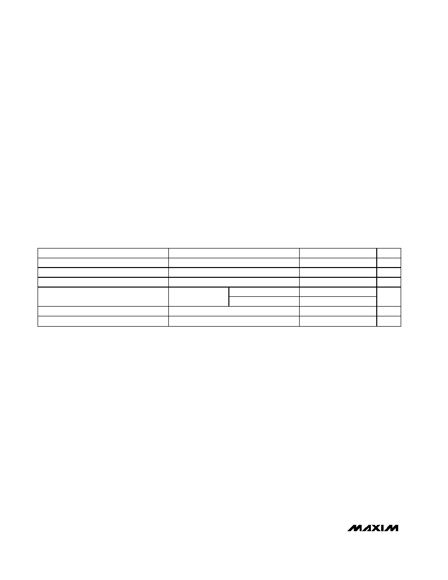
PARAMETER
CONDITIONS
MIN
TYP
MAX
UNITS
Idle Supply Current
MODE
= high
205
255
mA
Logic High Threshold
2.0
V
Logic Low Threshold
0.8
V
V
CC
= +2.8V to +4.0V
0.6
10
Shutdown Supply Current
SHDN = MODE
=
GND
V
CC
= +4.5V
60
120
µA
Logic High Input Current
5
µA
Logic Low Input Current
-1
+1
µA
DC ELECTRICAL CHARACTERISTICS
(V
CC
= +2.8V to +4.5V, no RF signal applied, SHDN = high, T
A
= -40°C to +85°C, unless otherwise noted. Typical values are mea-
sured at V
CC
= +3.3V and T
A
= +25°C.)

MAX2251
+2.8V, Single-Supply,
Cellular-Band Linear Power Amplifier
_______________________________________________________________________________________
3
AC CHARACTERISTICS, TDMA OPERATION
(MAX2251 EV kit, f
IN
= 824MHz to 849MHz, V
CC =
V
MODE
= V
SHDN
= +3.3V, 50
system, NADC modulation, duty cycle = 100%,
T
A
= +25°C, unless otherwise noted. Typical values are at f
IN
= 836MHz, T
A
= +25°C.) (Note 1)
Note 1: Guaranteed by design and characterization.
Note 2: Operation outside the frequency range is possible, but has not been characterized.
Note 3: Time when V
SHDN
transitions to V
CC
until P
OUT
is within 1dB of its final mean power.
Note 4: Harmonics are measured on the MAX2251 EV kit. The output matching provides some harmonic attenuation in addition to the
rejection provided by the IC. The combined suppression is specified.
Note 5: The range is defined by the difference between the rated linear output power and the output power that corresponds to
V
PD
= 0.57V.
Note 6: Time from when V
SHDN
transitions high until detector output reaches within 10% of its final value.
PARAMETER
CONDITIONS
MIN
-4.5
TYP
4.5
MAX
UNITS
Frequency Range (Note 2)
V
MODE
= V
CC
or GND
824
849
MHz
Power Gain
P
OUT
= +30dBm
25.7
26.1
27.8
dB
E xtr em e C ondi ti on P ow er Gai n
T
A
= -40°C to +85°C, P
OUT
= +30dBm
24.8
25.2
dB
Output Power
V
CC
= +3.3V, meets ACPR
specifications
30
dBm
T
A
= +25
o
C
-29.3/
-47.5
-27.4/
-45.4
-27/
-44.6
Adjacent/Alternate-Channel
Power Ratio
f
OFFSET
= 30/60kHz in
25kHz bandwidth
T
A
= +85°C
-28/
-48
dBc
AMPS Output Power
V
MODE
= V
CC,
P
IN
= +8dBm single tone
31.8
32
dBm
Power-Added Efficiency
P
OUT
= +30dBm
41.2
%
AM P S P ow er - Ad d ed E ffi ci ency
P
IN
= +8dBm single tone at 836MHz
51
%
Turn-On Time (Note 3)
2
5
µs
Input VSWR
1.2:1
1.76:1
Maximum Nonharmonic
Spurious Due to Load
Mismatch
V
CC
= +2.8V to +4.5V, all input power
levels, VSWR = 4:1 all phase angle,
T
A
= -40°C to +85°C
-55
dBc
Noise Power
f
RF
= 849MHz, noise measured at
869MHz, P
OUT
= +30dBm
-121
dBm/
Hz
AMPS Noise Power
f
RF
= 836MHz, noise measured at
881MHz, P
OUT
= +31dBm
-141
dBm/
Hz
H ar m oni c S up p r essi on ( N ote 4)
45
dBc
Power Detector Range
(Note 5)
27
29.4
dB
Power Detector Settling Time
( N ote 6)
C
DET
= 4700pF
2
3
µs

MAX2251
+2.8V, Single-Supply,
Cellular-Band Linear Power Amplifier
4
_______________________________________________________________________________________
0
10
5
20
15
35
30
25
40
2.8
3.6
4.5
SHUTDOWN vs. SUPPLY VOLTAGE
MAX2251-01
SUPPLY VOLTAGE (V)
SHUTDOWN CURRENT (nA)
T
A
= +25
°C
T
A
= -40
°C
T
A
= +85
°C
V
SHDN
= V
MODE
= GND
NO INPUT DRIVE
0
100
50
200
150
350
300
250
400
2.8
3.6
4.5
MAX2251-02
SUPPLY VOLTAGE (V)
QUIESCENT CURRENT (mA)
QUIESCENT CURRENT
vs. SUPPLY VOLTAGE
NO INPUT DRIVE
T
A
= +85
°C
T
A
= +25
°C
T
A
= -40
°C
0
200
100
400
300
700
600
500
800
2.8
3.6
4.5
MAX2251-03
SUPPLY VOLTAGE (V)
QUIESCENT CURRENT (mA)
QUIESCENT CURRENT
vs. SUPPLY VOLTAGE
V
MODE
= GND
NO INPUT DRIVE
T
A
= +25
°C
T
A
= +85
°C
T
A
= -40
°C
0
50
150
100
250
200
300
-10
-5
0
5
10
SUPPLY CURRENT
vs. OUTPUT POWER
MAX2251-04
OUTPUT POWER (dBm)
SUPPLY CURRENT (mA)
WITHOUT THROTTLEBACK
WITH THROTTLEBACK (MAINTAIN
ACPR = -29dBc, ALT <-50dBc)
20
22
28
26
24
30
10
15
20
25
30
GAIN vs. OUTPUT POWER
MAX2251-05
OUTPUT POWER (dBm)
GAIN (dB)
T
A
= +25°C
T
A
= -40°C
T
A
= +85°C
20
22
28
26
24
30
10
15
20
25
30
GAIN vs. OUTPUT POWER
MAX2251-06
OUTPUT POWER (dBm)
GAIN (dB)
V
CC
= +3.3V
V
CC
= +4.5V
V
CC
= +2.8V
20
22
24
28
26
30
824
829
834
839
844
849
GAIN vs. FREQUENCY
MAX2251-07
FREQUENCY (MHz)
GAIN (dB)
P
OUT
= +30dBm
T
A
= +25
°C
T
A
= -40
°C
T
A
= +85
°C
20
22
24
28
26
30
824
829
834
839
844
849
GAIN vs. FREQUENCY
MAX2251-08
FREQUENCY (MHz)
GAIN (dB)
V
CC
= V
MODE
= V
SHDN
= +2.8V
P
OUT
= +28dBm
20
22
24
26
32
28
30
34
824
829
834
839
844
849
GAIN vs. FREQUENCY AMPS
MAX2251-09
FREQUENCY (MHz)
GAIN (dB)
V
MODE
= GND
V
MODE
= V
CC
P
OUT
= +31dBm
Typical Operating Characteristics
(MAX2251 EV kit, V
CC =
V
MODE
= V
SHDN
= +3.3V, f
IN
= 836MHz, TDMA modulation, T
A
= +25°C, unless otherwise noted.)

MAX2251
+2.8V, Single-Supply,
Cellular-Band Linear Power Amplifier
_______________________________________________________________________________________
5
0
15
45
30
5
10
20
40
25
35
50
20
22
24
26
28
30
POWER-ADDED EFFICIENCY
vs. OUTPUT POWER
MAX2251-10
OUTPUT POWER (dBm)
PAE (%)
30
36
48
42
32
34
38
46
40
44
50
824
829
834
839
844
849
POWER-ADDED EFFICIENCY
vs. FREQUENCY
MAX2251-11
FREQUENCY (MHz)
PAE (%)
T
A
= +25
°C
V
CC
= +2.8V
P
O
= +28dBm
T
A
= +25
°C
T
A
= -40
°C
T
A
= +85
°C
P
OUT
= +30dBm
30
36
48
42
32
34
38
46
40
44
50
824
829
834
839
844
849
POWER-ADDED EFFICIENCY
vs. FREQUENCY, AMPS
MAX2251-12
FREQUENCY (MHz)
PAE (%)
V
MODE
= GND
V
MODE
= V
CC
P
OUT
= +31dBm
0
20
10
50
30
40
60
20
24
26
22
28
32
30
POWER-ADDED EFFICIENCY
vs. OUTPUT POWER, AMPS
MAX2251-13
OUTPUT POWER (dBm)
PAE (%)
V
MODE
= V
CC
-55
-45
-50
-30
-40
-35
-25
824
829
834
839
844
849
ACPR/ALT vs. FREQUENCY
MAX2251-14
FREQUENCY (MHz)
ACPR/ALT (dBc)
P
OUT
= +30dBm
ACPR
T
A
= +25°C
ACPR
T
A
= +85°C
ALT
T
A
= +85°C
ALT
T
A
= +25°C
-55
-45
-50
-30
-40
-35
-25
824
829
834
839
844
849
ACPR/ALT vs. FREQUENCY
MAX2251-15
FREQUENCY (MHz)
ACPR/ALT (dBc)
V
SHDN
= V
CC
= +2.8V
P
OUT
= +28dBm
ACPR
ALT
-60
-40
-45
-50
-55
-25
-35
-30
-20
20
22
24
26
28
30
ACPR/ALT vs. OUTPUT POWER
MAX2251-16
OUTPUT POWER (dBm)
ACPR/ALT (dBc)
f
IN
= 836MHz
ACPR
ALT
-170
-140
-150
-160
-110
-130
-120
-100
869
874
879
884
889
894
NOISE POWER vs. FREQUENCY
MAX2251-17
FREQUENCY (MHz)
NOISE POWER (dBm/Hz)
P
OUT
= +30dBm
T
A
= -40°C
f
IN
= 849MHz
f
IN
= 836MHz
f
IN
= 824MHz
-170
-140
-150
-160
-110
-130
-120
-100
869
874
879
884
889
894
NOISE POWER vs. FREQUENCY AMPS
MAX2251-18
FREQUENCY (MHz)
f
IN
= 849MHz
f
IN
= 836MHz
f
IN
= 824MHz
NOISE POWER (dBm/Hz)
P
OUT
= +32dBm
T
A
= -40°C
Typical Operating Characteristics (continued)
(MAX2251 EV kit, V
CC =
V
MODE
= V
SHDN
= +3.3V, f
IN
= 836MHz, TDMA modulation, T
A
= +25°C, unless otherwise noted.)