
For free samples & the latest literature: http://www.maxim-ic.com, or phone 1-800-998-8800.
For small orders, phone 1-800-835-8769.
General Description
The MAX2232/MAX2233 low-voltage, silicon RF power
amplifiers (PAs) are designed for use in the 900MHz
ISM band. They operate from a single +2.7V to +5.5V
supply, allowing them to be powered directly from a 3-
cell NiCd or a 1-cell Lithium-Ion battery. The devices
typically deliver 250mW (+24dBm) of output power at
915MHz from a single +3.6V supply, or 150mW
(+22dBm) from a single +2.7V supply. At +24dBm out-
put power, power-added efficiency (PAE) is 44%.
The MAX2232/MAX2233 provide 24dB of gain, which is
adjustable over a continuous 24dB span via the analog
gain-control pin of the MAX2232 or in two 10dB steps
via the 2-bit programmable gain-control DAC of the
MAX2233. An external capacitor sets the RF output
power envelope ramp time, reducing spurious emis-
sions during power-up and power-down by providing a
gradual change in output power (MAX2232).
The MAX2232/MAX2233 feature a low-power shutdown
mode, which typically draws less than 1µA of supply
current, saving power during "idle slots" in time-division
multiple-access (TDMA) systems. The
VSWR of the RF
input in shutdown mode relative to normal operation is
1.2:1. The devices also feature a thermal shutdown
function, enabling the PA to protect itself from excessive
temperature conditions that could damage the IC. A
capacitor to ground limits thermal cycling by setting a
thermal shutdown timeout period.
The MAX2232/MAX2233 are available in a space-sav-
ing, thermally enhanced 16-pin power-QSOP (PQSOP)
package.
Applications
900MHz ISM Band
Digital Cordless Phones
Wireless Data
FM Analog Transmitters
868MHz European ISM Band
Features
o
800MHz to 1000MHz Frequency Range
o
250mW (+24dBm) Output Power at 915MHz from
+3.6V Supply
o
+2.7V to +5.5V Single-Supply Operation
o
44% Power-Added Efficiency
o
24dB Power Gain
o
24dB Analog Gain-Control Range (MAX2232)
o
Three Levels of Digitally Programmed Power Gain
in 10dB Steps (MAX2233)
o
Programmable RF Power Envelope Ramping
(MAX2232)
o
Thermal Shutdown
o
Programmable Thermal Shutdown Timeout Period
o
0.2µA Low-Power Shutdown Mode
o
Low
VWSR in Standby and Shutdown Modes
MAX2232/MAX2233
900MHz ISM-Band, 250mW Power Amplifiers
with Analog or Digital Gain Control
________________________________________________________________
Maxim Integrated Products
1
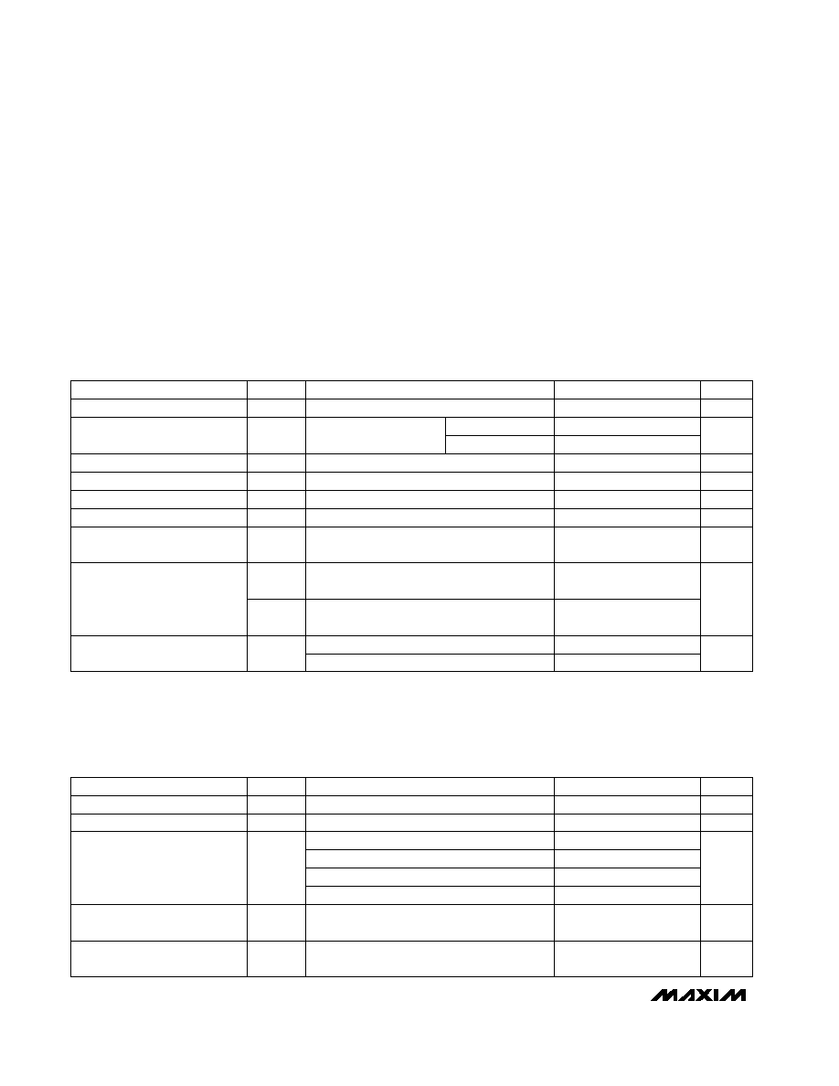
16
15
14
13
12
11
10
9
1
2
3
4
5
6
7
8
RFIN
V
CC
GND
RAMP+ (N.C.)
RAMP- (N.C.)
V
CC
V
CC
TSET
N.C.
TOP VIEW
MAX2232
MAX2233
PQSOP
GND
SHDN (D1)
GND
CTRL (D0)
GND
GND
RFOUT
GROUND OF OUTPUT STAGE CONNECTED TO PACKAGE SLUG.
( ) ARE FOR MAX2233.
19-1470; Rev 0; 4/99
PART
MAX2232
EEE
MAX2233
EEE
-40°C to +85°C
-40°C to +85°C
TEMP. RANGE
PIN-PACKAGE
16 PQSOP
16 PQSOP
Pin Configuration
Ordering Information
Functional Diagram appears at end of data sheet.
MAX2232/MAX2233
900MHz ISM-Band, 250mW Power Amplifiers
with Analog or Digital Gain Control
2
_______________________________________________________________________________________
ABSOLUTE MAXIMUM RATINGS
DC ELECTRICAL CHARACTERISTICS
(V
CC
= +2.7V to +5.5V, V
CTRL
= +2.2V, V
SHDN
= V
D0
= V
D1
= +2V, T
A
= -40°C to +85°C. No input signal applied, unless otherwise
noted. Typical values are at V
CC
= +3.6V and T
A
= +25°C.)
AC ELECTRICAL CHARACTERISTICS
(MAX2232/MAX2233 Evaluation Kit, V
CC
= +3.6V, V
CTRL
= +2.2V, SHDN = V
CC
(MAX2232), D0 = D1 = V
CC
(MAX2233),
P
RFIN
= 0dBm,
RFIN
= 915MHz, T
A
= +25°C, unless otherwise noted.)
Stresses beyond those listed under "Absolute Maximum Ratings" may cause permanent damage to the device. These are stress ratings only, and functional
operation of the device at these or any other conditions beyond those indicated in the operational sections of the specifications is not implied. Exposure to
absolute maximum rating conditions for extended periods may affect device reliability.
V
CC
to GND ...........................................................-0.3V to +6.5V
SHDN, CTRL, D0, D1 to GND ....................-0.3V to (V
CC
+0.3V)
I
RFIN
....................................................................................10mA
RFIN Power (50
AC-coupled source). .........................+10dBm
Output Load VSWR. ................................................................6:1
Continuous Power Dissipation (T
A
= +70°C)
16-Pin PQSOP (derate 80mW/°C above +70°C) ................3W
Operating Temperature Range ...........................-40°C to +85°C
Storage Temperature Range .............................-65°C to +150°C
Lead Temperature (soldering, 10sec) .............................+300°C
V
CTRL
0.4V (MAX2232)
V
SHDN
= 0.6V,
V
D0
= V
D1
= 0.6V
V
CTRL
= GND
V
SHDN
= GND (MAX2232),
V
D0
= V
D1
= GND (MAX2233)
V
SHDN
= 2.0V (MAX2232),
V
D0
= V
D1
= 2.0V (MAX2233)
MAX2232
SHDN (MAX2232), D0, D1 (MAX2233)
SHDN (MAX2232), D0, D1 (MAX2233)
MAX2232
V
CTRL
= 2.2V
CONDITIONS
1.5
mA
20.3
25
I
CC
Standby Supply Current
0.2
10
I
CC
V
2.7
5.5
V
CC
Supply Voltage Range
Shutdown Supply Current
µA
-1.5
1
CTRL Input Current
-1
1
I
IL
µA
-1
10
I
IH
Logic Input Current
V
0.6
V
CTRL
CTRL Input for Gain-Control
Mode
V
2.0
V
IH
Logic Input High
V
0.6
V
IL
Logic Input Low
V
0.4
V
CTRL
CTRL Input for Standby Mode
UNITS
MIN
TYP
MAX
SYMBOL
PARAMETER
µA
7.5
V
CC
4.8V
4.8V < V
CC
5.5V
V
CC
= 4.8V
(Notes 1, 2)
D0 = GND, D1 = V
CC
(MAX2233 only)
V
CC
= 3.6V (Note 1)
V
CC
= 3.0V
V
CC
= 2.7V
T
A
= T
MIN
to T
MAX
(Note 1)
CONDITIONS
25.4
dB
23.9
G
P
MHz
902
928
IN
Frequency Range
Power Gain
dBm
15.8
P
OUT
Output Power, Medium-Power
Mode
22.9
23.9
24.9
dBm
22.5
21.6
P
OUT
Output Power
dB
1.9
3.2
P
OUT
Output Power Variation Over
Temperature
UNITS
MIN
TYP
MAX
SYMBOL
PARAMETER
MAX2232/MAX2233
900MHz ISM-Band, 250mW Power Amplifiers
with Analog or Digital Gain Control
_______________________________________________________________________________________
3
AC ELECTRICAL CHARACTERISTICS (continued)
(MAX2232/MAX2233 Evaluation Kit, V
CC
= +3.6V, V
CTRL
= +2.2V, SHDN = V
CC
(MAX2232), D0 = D1 = V
CC
(MAX2233),
P
RFIN
= 0dBm,
RFIN
= 915MHz, T
A
= +25°C, unless otherwise noted.)
Note 1:
Guaranteed by design.
Note 2:
Operation outside this range is possible, but not characterized.
Note 3:
Gain is monotonic with V
CTRL
.
Note 4:
Input VSWR relative to input impedance in operating mode.
Note 5:
Harmonics measured on evaluation kit, which provides some harmonic attenuation in addition to the rejection provided by
the IC. The combined suppression is specified.
Note 6:
Time measured from SHDN (MAX2232) low-to-high transition to when output power is within 1dB of final value. Includes
effects of 1% tolerance capacitor.
Note 7:
Time measured from SHDN (MAX2232) high-to-low transition to when output power is -20dB of final value. Includes effects
of 1% tolerance capacitors.
Note 8:
Time from die temperature dropping below Thermal Shutdown Temperature, T
TH
, to when the device turns itself back on.
C
RAMP
= 0.22µF (Notes 1, 6) (MAX2232 only)
(Note 5)
Any load phase angle, P
RFIN
= +5dBm,
T
A
= T
MIN
to T
MAX
V
CC
= +2.7V to +5.5V,
6:1 VSWR at any phase angle,
P
RFIN
= +5dBm
CTRL = GND (MAX2232 only)
SHDN = D0 = D1 = GND
MAX2232 only
0.6V < V
CTRL
< 2.2V (MAX2232 only)
Z
SOURCE
= 50
(Note 1)
D0 = V
CC
, D1 = GND (MAX2233 only)
D0 = V
CC
, D1 = GND (MAX2233 only)
D0 = GND, D1 = V
CC
(MAX2233 only)
CTRL adjusted to give P
RFOUT
= +21dBm
(MAX2232 only)
CONDITIONS
ms
0.9
Autoramping Rise Time
dBc
29
Harmonic Suppression
6:1
Maximum Output Load VSWR
Without Damage (Note1)
dBc
-60
Maximum Nonharmonic
Spurious Output Due to Load
Mismatch
dB
38
52
Off-Isolation
1.2:1
VSWR
Input VSWR Change, Standby
Mode (Notes 1, 4)
1.4:1
VSWR
Input VSWR Change, Shutdown
Mode (Notes 1, 4)
1.5:1
VSWR
Input VSWR
mA
44.0
I
CC
Supply Current, Low-Power
Mode
mA
78.5
I
CC
Supply Current, Medium-Power
Mode
%
29
PAE
Power-Added Efficiency at
+21dBm Output Power
%
44
PAE
Power-Added Efficiency
dB
23.6
G
P
Gain-Control Range (Note 3)
dBm
6.5
P
OUT
Output Power, Low-Power Mode
UNITS
MIN
TYP
MAX
SYMBOL
PARAMETER
P
RFIN
= 0dBm, V
CC
= +3.6V
RAMP+ = RAMP- = unconnected (Note 6)
C
RAMP
= 0.22µF (Notes 1, 7) (MAX2232 only)
C
TSET
= 0.22µF (Note 8)
°C
145
T
TH
Thermal Shutdown Temperature
µs
0.4
ms
3.2
Autoramping Fall Time
Output Power Rise Time
ms
900
t
TH
Thermal Shutdown Timeout
Period
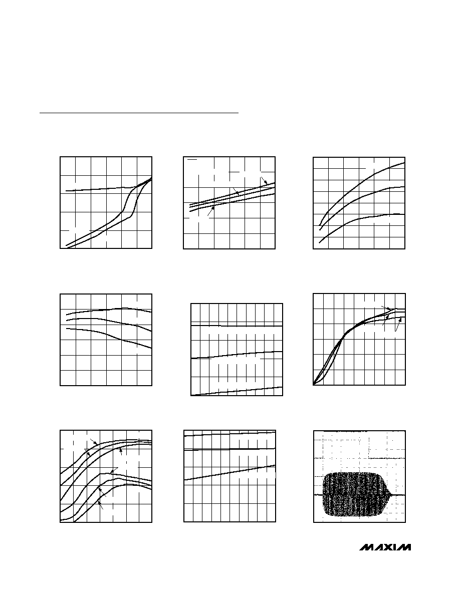
LINEAR
SCALE
0
3V
1ms/div
MAX2232
OUTPUT POWER vs. SHUTDOWN CONTROL
MAX2232/33 toc10
C
RAMP
= 0.22
µ
F
OUTPUT
POWER
SHUTDOWN
MAX2232/MAX2233
900MHz ISM-Band, 250mW Power Amplifiers
with Analog or Digital Gain Control
4
_______________________________________________________________________________________
Typical Operating Characteristics
(MAX2232/MAX2233 Evaluation Kit, V
CC
= +3.6V, CTRL = V
CC
, SHDN = D0 = D1 = V
CC
, P
RFIN
= 0dBm, f
RFIN
= 915MHz, T
A
= +25°C,
unless otherwise noted.)
0.001
0.01
1
0.1
10
100
2.5
3.5
3.0
4.0
4.5
5.0
5.5
SHUTDOWN SUPPLY CURRENT
vs. SUPPLY VOLTAGE
MAX2232/33 toc01
SUPPLY VOLTAGE (V)
SHUTDOWN SUPPLY CURRENT (
µ
A)
T
A
= -40°C
T
A
= +25°C
T
A
= +85°C
0
10
5
20
15
25
30
2.5
3.5
4.0
3.0
4.5
5.0
5.5
MAX2232
STANDBY SUPPLY CURRENT
vs. SUPPLY VOLTAGE
MAX2232/33 toc02
SUPPLY VOLTAGE (V)
SUPPLY CURRENT (mA)
T
A
= -40°C
T
A
= +25°C
T
A
= +85°C
V
SHDN
= V
CC
V
CTRL
= GND
RFIN = UNCONNECTED
22
23
24
25
26
27
28
20
21
2.5
3.5
3.0
4.0
4.5
5.0
5.5
OUTPUT POWER vs. SUPPLY VOLTAGE
MAX2232/33 toc03
SUPPLY VOLTAGE (V)
OUTPUT POWER (dBm)
T
A
= +85°C
T
A
= -40°C
T
A
= +25°C
0
5
10
15
20
25
30
0.6
1.0
0.8
1.2 1.4 1.6 .1.8 2.0 2.2 2.4
MAX2232
OUTPUT POWER vs. GAIN CONTROL VOLTAGE
MAX2232/33 toc06
V
CTRL
(V)
OUTPUT POWER (dBm)
T
A
= -40°C
T
A
= +25°C
T
A
= +85°C
10
0
20
40
30
50
60
2.5
3.5
3.0
4.0
4.5
5.0
5.5
POWER-ADDED EFFICIENCY
vs. SUPPLY VOLTAGE
MAX2232/33 toc04
SUPPLY VOLTAGE (V)
POWER-ADDED EFFICIENCY (%)
T
A
= -40°C
T
A
= +25°C
T
A
= +85°C
5
10
15
20
25
30
902
915
928
OUTPUT POWER vs. FREQUENCY
MAX2232/33 toc05
OUTPUT POWER (dBm)
MAX2233 (D0 = 0, D1 = 1)
MAX2233 (D0 = D1 = 1), AND MAX2232
MAX2233 (D0 = 1, D1 = 0)
3
8
18
13
23
28
10
25
55
40
70
85
-20
-10
-15
-5
0
5
10
15
OUTPUT POWER AND POWER-ADDED EFFICIENCY
vs. INPUT POWER
MAX2232/33 toc07
INPUT POWER (dBm)
OUTPUT POWER (dBm)
PAE (%)
T
A
= -40°C
T
A
= -40°C
T
A
= +25°C
P
OUT
PAE
T
A
= +25°C
T
A
= +85°C
T
A
= +85°C
1.0
1.2
1.4
1.6
1.8
2.0
902
915
928
MAX2232
RFIN PORT VSWR vs. FREQUENCY
MAX2232/33 toc08
FREQUENCY (MHz)
VSWR
SHUTDOWN MODE
NORMAL OPERATION
STANDBY MODE

MAX2232/MAX2233
900MHz ISM-Band, 250mW Power Amplifiers
with Analog or Digital Gain Control
_______________________________________________________________________________________
5
Pin Description
PIN
FUNCTION
MAX2232
MAX2233
13
--
Negative Terminal of Output Power Ramp Capacitor. Connect capacitor, C
RAMP
, between
RAMP+ and RAMP- to control the rise and fall time of the output power ramp.
12
12
Input Stage Supply Voltage. Bypass with appropriate capacitors to GND.
11
11
Second Stage Supply Voltage. Bypass with appropriate capacitors to GND.
10
10
Thermal Shutdown Timeout Capacitor Terminal. Connect a capacitor from TSET to ground
to limit thermal cycling.
9
9, 13, 14
No Connection. Do not make a connection to this pin.
14
--
Positive Terminal of Output Power Ramp Capacitor. Connect capacitor, C
RAMP
, between
RAMP+ and RAMP- to control the rise and fall time of the output power ramp.
15
15
Bias Circuitry Ground. Connect directly to low-inductance ground plane. If vias are used,
separate them from other GND pin vias.
16
16
Bias Circuitry Supply Voltage. Bypass with appropriate capacitors to GND.
SLUG
SLUG
Output Stage Ground. Provides additional thermal conduction, as well as a low-inductance
path to ground. Connect directly to low-inductance ground plane.
NAME
RAMP-
V
CC
V
CC
TSET
N.C.
RAMP+
GND
V
CC
GND
8
8
Open-Collector, RF Output Port. Connect output matching network to this pin.
RFOUT
5, 6
5, 6
Second Stage Ground. Connect directly to low-inductance ground plane. If vias are used,
separate them from other GND pin vias.
GND
7
7
Output Stage Ground. Connect directly to low-inductance ground plane. If vias are used,
separate them from other GND pin vias.
GND
4
--
Analog Gain-Control Input. Apply a voltage between 0.6V and 2.2V to vary the gain of the
PA. Drive CTRL below 0.4V to place the device in standby mode. Drive CTRL above 2.2V to
place the device in peak output power mode.
CTRL
3
--
Shutdown Control Input. Drive SHDN low to place the device in shutdown mode. Drive high
for normal operation.
SHDN
--
3
Digital Gain/Shutdown Control Input. MSB of the 2-bit digital output power control. D0 and
D1 set the output power to one of three discrete levels. To place the device in shutdown,
drive D0 and D1 low (Table 2).
D1
--
4
Digital Gain/Shutdown Control Input. LSB of the 2-bit digital output power control. D0 and
D1 set the output power to one of three discrete levels. To place the device in shutdown,
drive D0 and D1 low (Table 2).
D0
1
1
RF Input Port. Requires external matching network and blocking capacitor.
RFIN
2
2
Input Stage Ground. Connect directly to low-inductance ground plane. If vias are used,
separate them from other GND pin vias.
GND