Äîêóìåíòàöèÿ è îïèñàíèÿ www.docs.chipfind.ru
General Description
The MAX2205MAX2208 wideband (800MHz to 2GHz)
power detectors are ideal for GSM/EDGE (MAX2206),
TDMA (MAX2207), and CDMA (MAX2205/MAX2208)
applications. The MAX2206/MAX2207/MAX2208 take an
RF signal from a directional coupler at the input, and out-
put a highly repeatable voltage. The output voltage
increases monotonically with increasing input power. The
output is compensated for temperature and process
shifts, reducing the worst-case variation to less than
±1dB at full power and ±2.5dB at the lowest power.
The MAX2206 features 40dB dynamic range, making
it ideally suited to GSM/EDGE applications. The
MAX2207 offers reduced current consumption for TDMA
applications. The MAX2205/MAX2208 each have an inte-
grated filter to allow for average power detection of
CDMA signals over a 25dB dynamic range. The
MAX2206/MAX2207/MAX2208 offer internal 50
termina-
tion for interfacing with a directional coupler. The
MAX2205 has a high-impedance input to provide a low-
loss resistive tap in CDMA applications. All devices allow
the user to control the averaging time constant externally.
The MAX2205MAX2208 come in a space-saving 2
2,
0.5mm-pitch UCSPTM and require only three external
components.
Applications
Dual-Band GSM/EDGE Handsets
Dual-Band CDMA/TDMA Handsets
WCDMA Handsets
PA Modules
Features
o Space-Saving 2
2 UCSP Occupies Only 1mm
2
o Internal Temperature Compensation Gives ±0.3dB
Detection Accuracy
o No External Filter or Op Amp Required
o Power-Detection Range
40dB (MAX2206)
25dB (MAX2205/MAX2207/2208)
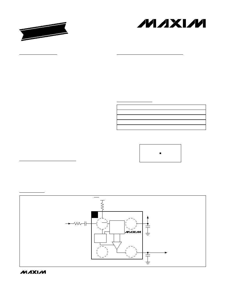
MAX2205MAX2208
RF Power Detectors in UCSP
________________________________________________________________ Maxim Integrated Products
1
TOP VIEW
GND
(B1)
OUT
(B2)
TEMPERATURE-
COMPENSATED
PEAK
DETECTOR
SHUTDOWN
LOGIC
UCSP
TO ADC
10k
(MAX2205)
240
(MAX2206/MAX2207/MAX2208)
27pF
680
(MAX2205)
10
(MAX2206)
0
(MAX2207/MAX2208)
47pF
FROM COUPLER/TAP
(MAX2206/MAX2207/MAX2208)
MAX2205
MAX2206
MAX2207
MAX2208
SHDN LOGIC INPUT
RFIN/SHDN
(A1)
V
CC
(A2)
V
CC
C
FILTER
(OPTIONAL)
FROM PA OUTPUT
(MAX2205)
Pin Configuration/Functional Diagram/Typical Operating Circuit
19-2015; Rev 2; 8/02
For pricing, delivery, and ordering information, please contact Maxim/Dallas Direct! at
1-888-629-4642, or visit Maxim's website at www.maxim-ic.com.
EVALUATION KIT
AVAILABLE
Ordering Information
UCSP is a trademark of Maxim Integrated Products, Inc.
*Requires solder temperature profile described in the Absolute
Maximum Ratings section.
PART
TEMP RANGE
BUMP-PACKAGE
MAX2205EBS
-40°C to +85°C
2
× 2 UCSP*
MAX2206EBS
-40°C to +85°C
2
× 2 UCSP*
MAX2207EBS
-40°C to +85°C
2
× 2 UCSP*
MAX2208EBS
-40°C to +85°C
2
× 2 UCSP*
2
2 UCSP
1.01 mm
1.01 mm
MAX2205MAX2208
RF Power Detectors in UCSP
2
_______________________________________________________________________________________
ABSOLUTE MAXIMUM RATINGS
DC ELECTRICAL CHARACTERISTICS (MAX2205MAX2208)
(V
CC
= +2.7V to +5.0V, SHDN = +2.0V, no RF signal applied, T
A
= -40°C to +85°C. Typical values are at V
CC
= +2.85V and
T
A
= +25°C, unless otherwise noted.) (Note 2)
Stresses beyond those listed under "Absolute Maximum Ratings" may cause permanent damage to the device. These are stress ratings only, and functional
operation of the device at these or any other conditions beyond those indicated in the operational sections of the specifications is not implied. Exposure to
absolute maximum rating conditions for extended periods may affect device reliability.
V
CC
to GND ...........................................................-0.3V to +6.5V
RFIN/SHDN to GND....................................-0.3V to (V
CC
+ 0.3V)
RF Input Power (800MHz)
(MAX2206/MAX2207/MAX2208) .................................+20dBm
RF Input Power (2GHz)
(MAX2206/MAX2207/MAX2208) .................................+17dBm
RF Input Voltage (800MHz) (MAX2205) ..............................1.5V
P
RF Input Voltage (2GHz) (MAX2205) ..................................0.8V
P
Continuous Power Dissipation (T
A
= +70°C)
2
2 UCSP (derate 3.8mW/°C above +70°C) ............303mW
Operating Temperature Range ...........................-40°C to +85°C
Junction Temperature ......................................................+150°C
Storage Temperature Range .............................-65°C to +160°C
Bump Temperature (soldering) (Note 1)
Infrared (15s) ..............................................................+220°C
Vapor Phase (60s) ......................................................+215°C
PARAMETER
SYMBOL
CONDITIONS
MIN
TYP
MAX
UNITS
Supply Voltage
V
CC
2.7
5.0
V
MAX2206
3.5
5.5
Idle Supply Current
I
IDLE
MAX2205/MAX2207/MAX2208
2
3.5
mA
Shutdown Supply Current
I
SHDN
SHDN = 0V
0.5
10
µA
OUT Voltage During Shutdown
V
OUT
SHDN = 0V
0.01
V
Logic-High Threshold
V
H
2.0
V
Logic-Low Threshold
V
L
0.6
V
I
IH
SHDN = +2.0V
-1
+10
SHDN Input Current
I
IL
SHDN = +0.6V
-1
+1
µA
Output Current Source Capability
MAX2206/MAX2207, V
OUT
= +2.5V
400
µA
Output Current Sink Capability
MAX2206/MAX2207, V
OUT
= 0V
300
µA
AC ELECTRICAL CHARACTERISTICS (MAX2205)
(MAX2205 EV kit, V
CC
= +2.7V to +5.0V, SHDN = +2.0V, f
RF
= 800MHz to 2GHz, 50
system, T
A
= -40
°C to +85°C. Typical values
are at V
CC
= +2.85V and T
A
= +25°C, unless otherwise noted.) (Note 2)
PARAMETER
SYMBOL
CONDITIONS
MIN
TYP
MAX
UNITS
RF Input Frequency
f
RF
800
2000
MHz
Turn-On Time
t
ON
2
µs
Response Time
t
R
(Note 3)
15
µs
High input power
(Note 4)
±0.3
±1
Variation Due to Temperature
V
CC
= +2.85V,
T
A
= -40
°C to +85°C Low input power
(Note 5)
±1.3
±2.5
dB
MAX2205MAX2208
RF Power Detectors in UCSP
_______________________________________________________________________________________
3
Note 1: This device is constructed using a unique set of packaging techniques that imposes a limit on the thermal profile the device
can be exposed to during board-level solder attach and rework. This limit permits only the use of the solder profiles recom-
mended in the industry-standard specification, JEDEC 020A, paragraph 7.6, Table 3 for IR/VPR and convection reflow.
Preheating is required. Hand or wave soldering is not allowed.
Note 2: Specifications over T
A
= -40°C to +85°C are guaranteed by design. Production tests are performed at T
A
= +25°C.
Note 3: Response time is taken from the time the RF signal is applied to 90% of the final value of V
OUT
.
Note 4: At 800MHz, output voltage is held at a value that nominally results from the final value of +31dBm input power. Deviation from
+31dBm is specified. At 2GHz, output voltage is held at a value that nominally results from +28dBm input power. Deviation
from +28dBm is specified.
Note 5: At 2GHz, output voltage is held 22dB lower than specified in Note 4. At 800MHz, output voltage is held 25dB lower than spec-
ified in Note 4.
Note 6: At 800MHz, output voltage is held at a value that nominally results from +15dBm input power. Deviation from +15dBm is
specified. At 2GHz, output voltage is held at a value that nominally results from +13dBm input power. Deviation from +13dBm
is specified.
Note 7: For MAX2206, output voltage is held 40dB lower than specified in Note 7; for MAX2207/MAX2208, output voltage is held 25dB
lower than specified in Note 7.
AC ELECTRICAL CHARACTERISTICS (MAX2206/MAX2207/MAX2208)
(MAX2206/MAX2207/MAX2208 EV kit, V
CC
= +2.7V to +5.0V, SHDN = 2.0V, f
RF
= 800MHz to 2GHz, 50
system, T
A
= -40
°C to
+85°C. Typical values are at V
CC
= +2.85V and T
A
= +25°C, unless otherwise noted.) (Note 2)
PARAMETER
SYMBOL
CONDITIONS
MIN
TYP
MAX
UNITS
RF Input Frequency
f
RF
800
2000
MHz
RF Input VSWR
VSWR
2:1
Turn-On Time
t
ON
2
µs
MAX2206/MAX2207
300
ns
Response Time (Note 3)
t
R
MAX2208
15
µs
H i g h i np ut p ow er ( N ote 6)
±0.3
±1
Variation Due to Temperature
V
CC
= +2.85V,
T
A
= -40°C to +85°C
Low i np ut p ow er ( N ote 7)
±1.3
±2.5
dB
Typical Operating Characteristics
(MAX2206/MAX2207/MAX2208 EV kit, T
A
= +25°C, unless otherwise noted.)
0
0.4
0.2
0.8
0.6
1.2
1.0
1.4
1.8
1.6
2.0
-25
-15
-10
-20
-5
0
5
10
15
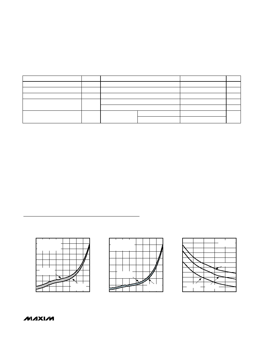
MAX2206
OUTPUT VOLTAGE vs. INPUT POWER
MAX2205/06/07/08 toc01
POWER (dBm)
OUTPUT VOLTAGE (V)
V
CC
= +2.7V to +3.5V
f
RF
= 800MHz
T
A
= -40
°C TO +85°C
V
CC
= +3.5V
T
A
= +85
°C
V
CC
= +2.7V
T
A
= -40
°C
0
0.4
0.2
0.8
0.6
1.0
1.2
1.4
1.6
-25
-15
-10
-20
-5
0
5
10
15
MAX2206
OUTPUT VOLTAGE vs. INPUT POWER
MAX2205/06/07/08 toc02
POWER (dBm)
OUTPUT VOLTAGE (V)
V
CC
= +2.7V to +3.5V
f
RF
= 2GHz
T
A
= -40
°C TO +85°C
V
CC
= +3.5V
T
A
= +85
°C
V
CC
= +2.7V
T
A
= -40
°C
265
270
275
280
285
290
295
300
305
310
315
320
-40
-15
10
35
60
85
MAX2206
RESPONSE TIME vs. TEMPERATURE
MAX2205/06/07/08 toc03
TEMPERATURE (
°C)
RESPONSE TIME (ns)
V
CC
= +2.7V
V
CC
= +3.5V
V
CC
= +3.0V
f
RF
= 900MHz
P
IN
= +15dBm
MAX2205MAX2208
RF Power Detectors in UCSP
4
_______________________________________________________________________________________
0
0.5
1.5
1.0
2.0
2.5
-10
0
-5
5
10
15
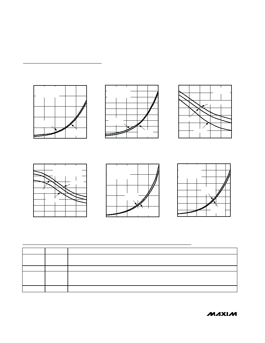
MAX2207/MAX2208
OUTPUT VOLTAGE vs. INPUT POWER
MAX2205/06/07/08 toc04
POWER (dBm)
OUTPUT VOLTAGE (V)
V
CC
= +2.7V to +3.5V
f
RF
= 800MHz
T
A
= -40
°C TO +85°C
V
CC
= +3.5V
T
A
= +85
°C
V
CC
= +2.7V
T
A
= -40
°C
0
0.4
0.2
1.0
0.8
0.6
1.6
1.4
1.2
1.8
-10
0
-5
5
10
15
MAX2207/MAX2208
OUTPUT VOLTAGE vs. INPUT POWER
MAX2205/06/07/08 toc05
POWER (dBm)
OUTPUT VOLTAGE (V)
V
CC
= +2.7V to +3.5V
f
RF
= 2GHz
T
A
= -40
°C TO +85°C
V
CC
= +3.5V
T
A
= +85
°C
V
CC
= +2.7V
T
A
= -40
°C
275
285
280
295
290
305
300
310
-40
10
-15
35
60
85
MAX2207
RESPONSE TIME vs. TEMPERATURE
MAX2205/06/07/08 toc06
TEMPERATURE (
°C)
RESPONSE TIME (ns)
f
RF
= 900MHz
P
IN
= +15dBm
V
CC
= +3.5V
V
CC
= +3.0V
V
CC
= +2.7V
10
12
11
15
14
13
18
17
16
19
-40
10
-15
35
60
85
MAX2205/MAX2208
RESPONSE TIME vs. TEMPERATURE
MAX2205/06/07/08 toc07
TEMPERATURE (
°C)
RESPONSE TIME (
µ
s)
f
RF
= 900MHz
P
IN
= +15dBm (MAX2208)
P
IN
= +31dBm (MAX2205)
V
CC
= +2.7V
V
CC
= +3.0V
V
CC
= +3.5V
0
0.5
1.5
1.0
2.0
2.5
6
16
11
21
26
31
MAX2205
OUTPUT VOLTAGE vs. INPUT POWER
MAX2205/06/07/08 toc08
INPUT POWER (dBm)
OUTPUT VOLTAGE (V)
V
CC
= +2.7V to +3.5V
f
RF
= 836MHz
T
A
= -40
°C to +85°C
MAX2205 EV KIT
V
CC
= +3.5V
T
A
= +85
°C
V
CC
= +2.7V
T
A
= -40
°C
0
0.3
0.2
0.1
0.5
0.4
0.6
0.7
0.8
6
14
18
10
22
26
MAX2205
OUTPUT VOLTAGE vs. INPUT POWER
MAX2205/06/07/08 toc09
INPUT POWER (dBm)
OUTPUT VOLTAGE (V)
V
CC
= +2.7V to +3.5V
f
RF
= 1880MHz
T
A
= -40
°C to +85°C
MAX2205 EV KIT
V
CC
= +3.5V
T
A
= +85
°C
V
CC
= +2.7V
T
A
= -40
°C
Typical Operating Characteristics (continued)
(MAX2206/MAX2207/MAX2208 EV kit, T
A
= +25°C, unless otherwise noted.)
Pin Description
PIN
NAME
FUNCTION
A1
RFIN/
SHDN
RF Input and Shutdown Logic Input. AC-couple the RF input to this pin and apply the shutdown logic
input through a resistor. Drive low to turn the part off, drive high, or connect to V
CC
to turn the part on.
A2
V
CC
Power-Supply Pin. Bypass to GND with a capacitor as close to the bump as possible.
B1
GND
Ground Connection. Multiple ground vias placed as close to the IC as possible should be used to
connect the ground pin to the ground plane. Connect to PC board ground plane with as low
inductance as possible.
B2
OUT
Detector Output
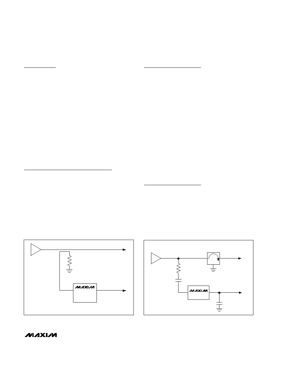
Applications Information
The MAX2205MAX2208 have internal termination
resistors for use with directional couplers. The applica-
tion circuit is shown in Figure 1. The output of the
detector goes to an op amp in an analog GSM power-
control scheme, or to an ADC in other systems such as
TDMA or discrete-time GSM power control.
The MAX2205 has high-input impedance for use with
high-value resistive tapping from a CDMA power ampli-
fier. This coupling method is the lowest cost and lowest
loss when used with an isolator. The application circuit
is shown in Figure 2. Connect C
FILTER
from the
MAX2205 output to GND to reduce residual amplitude
ripple. For IS98A reverse channel signal with peak-to-
avg ratio of 3.9dB, a 1.5nF capacitor gives 43mV
P-P
rip-
ple at 28dBm PA output and 390µs response time. For
CDMA2000 (pilot + DCCH) with peak-to-avg ratio of
5.4dB, the ripple is about 65mV
P-P
at 26dBm PA output.
The MAX2205 input impedance is listed in Table 1.
Layout
As with any RF circuit, the layout of the MAX2205
MAX2208 circuits affects performance. Use a short
50
line at the input with multiple ground vias along the
length of the line. The input capacitor and resistor
should be placed as close to the IC as possible. The
V
CC
input should be bypassed as close as possible to
the IC with multiple vias connecting the capacitor to
ground. Refer to the MAX2205MAX2208 EV kit data
sheet for a sample layout and details.
UCSP Reliability
The UCSP is a unique package that greatly reduces
board space compared to other packages. UCSP relia-
bility is integrally linked to the user's assembly methods,
circuit board material, and usage environment. The user
should closely review these areas when considering
using a UCSP. This form factor might not perform equally
to a packaged product through traditional mechanical
reliability tests. Performance through operating life test
and moisture resistance remains uncompromised, as it
is determined primarily by the wafer-fabrication process.
Mechanical stress performance is a greater considera-
tion for a UCSP. UCSP solder-joint contact integrity must
be considered because the package is attached through
direct solder contact to the user's PC board. Testing
done to characterize the UCSP reliability performance
shows that it is capable of performing reliably through
environmental stresses. Results of environmental stress
tests and additional usage data and recommendations
are detailed in the UCSP application note, which can be
found on Maxim's website, www.maxim-ic.com.
Chip Information
TRANSISTOR COUNT: 344
MAX2205MAX2208
RF Power Detectors in UCSP
_______________________________________________________________________________________
5
TO ANT
PA
C
FILTER
TO ADC
ISOLATOR/
CIRCULATOR
PEAK
DETECTOR
47pF
680
MAX2205
TO ANT
PA
TO ADC
OR OP AMP
50
PEAK
DETECTOR
COUPLER
MAX2206
MAX2207
MAX2208
Figure 2. MAX2205 Typical Application Circuit
Figure 1. MAX2206/MAX2207/MAX2208 Typical Application
Circuit