
_______________General Description
The MAX214 +5V RS-232 transceiver provides a com-
plete, 8-line, software-configurable, DTE or DCE port
RS-232 interface. Tx, Rx, RTS, CTS, DTR, DSR, DCD,
and RI circuits can be configured as either Data
Terminal Equipment (DTE) or Data Circuit-Terminating
Equipment (DCE) using the DTE/DCE control pin. The
MAX214 eliminates the need to swap cables when
switching between DTE and DCE configurations.
________________________Applications
AT-Compatible Laptop Computers
AT-Compatible Desktop Computers
Modems, Printers, and Other Peripherals
____________________________Features
o
Eliminates Null Modem Cables
o
Programmable DTE or DCE Serial Port
o
1µF Charge-Pump Capacitors
o
116kbps Data Rate--Guaranteed
o
20µA Shutdown Mode
o
Receivers Active in Shutdown
______________Ordering Information
* Dice are specified at T
A
= +25°C.
MAX214
Programmable DTE/DCE,
+5V RS-232 Transceiver
________________________________________________________________
Maxim Integrated Products
1
28
27
26
25
24
23
22
21
20
19
18
17
16
15
1
2
3
4
5
6
7
8
9
10
11
12
13
14
TOP VIEW
MAX214
C1-
C1+
SHDN
TB
TC
RB
RC
DTE/DCE
TRB
RTB
TRC
RTC
V
CC
V+
C2+
C2-
HI-Z
N.C.
TA
RA
RDC
RE
TRA
RTA
RDTC
RRE
GND
V-
DIP/SO
__________________Pin Configuration
RTA
V
CC
TRA
TRB
RTB
TRC
RTC
RDTC
RRE
RE
RC
TC
RB
TB
RA
TA
C1+
C1-
C2+
C2-
V+
V-
15
14
9
10
20
19
18
17
11
12
5
6
25
23
24
22
7
8
27
28
1
2
16
GND
13
1
µ
F
1
µ
F
1
µ
F
1
µ
F
+5V
DTE
DTE
DCE
DTE
DTE
DCE
DTE
DTE
DCE
DTE
DTE
DCE
DTE/DCE
SHDN
HI-Z
21
26
3
RDC
DCE
MAX214
1
µ
F
__________Typical Operating Circuit
Call toll free 1-800-998-8800 for free samples or literature.
PART
TEMP. RANGE
PIN-PACKAGE
MAX214CPI
0°C to +70°C
28 Plastic DIP
MAX214CWI
0°C to +70°C
28 Wide SO
MAX214C/D
0°C to +70°C
Dice*
MAX214EPI
-40°C to +85°C
28 Plastic DIP
MAX214EWI
-40°C to +85°C
28 Wide SO
19-0199; Rev 1; 8/95
MAX214
Programmable DTE/DCE,
+5V RS-232 Transceiver
2
_______________________________________________________________________________________
ABSOLUTE MAXIMUM RATINGS
V
CC
...........................................................................-0.3V to +6V
Input Voltages
T
IN
, DTE/DCE, SHDN HI-Z ......................-0.3V to (V
CC
+ 0.3V)
R
IN
....................................................................................±15V
Output Voltages:
T
OUT
..................................................................................±15V
R
OUT
........................................................-0.3V to (V
CC
+ 0.3V)
Short-Circuit (one output at a time)
T
OUT
to GND ...........................................................Continuous
R
OUT
to GND...........................................................Continuous
Continuous Power Dissipation (T
A
= +70°C)
Plastic DIP (derate 9.09mW/°C above +70°C) .............727mW
Wide SO (derate 12.50mW/°C above +70°C) ............1000mW
Operating Temperature Ranges:
MAX214CI ..............................................0°C to +70°C
MAX214EI ..........................................-40°C to +85°C
Storage Temperature Range ......................-65°C to +150°C
Lead Temperature (soldering, 10sec) .......................+300°C
ELECTRICAL CHARACTERISTICS
(V
CC
= 4.5V to 5.5V, C1 to C4 = 1
µ
F, T
A
= T
MIN
to T
MAX
, unless otherwise noted.)
Stresses beyond those listed under "Absolute Maximum Ratings" may cause permanent damage to the device. These are stress ratings only, and functional
operation of the device at these or any other conditions beyond those indicated in the operational sections of the specifications is not implied. Exposure to
absolute maximum rating conditions for extended periods may affect device reliability.
PARAMETER
MIN
TYP
MAX
UNITS
Output Short-Circuit Current
±7
±25
mA
Transmitter Output Resistance
300
300k
Output Voltage Swing
±5.0
±7.5
V
Logic Input Pull-Up Current
1
10
50
µ
A
Input Voltage Operating Range
±15
V
Positive Threshold Input Low
0.8
1.3
V
Positive Threshold Input High
1.8
2.4
V
Logic Input Threshold Low
0.8
1.4
V
Logic Input Threshold High
1.4
2.0
V
0.2
0.5
1.0
V
Negative Threshold Input Low
0.8
1.3
V
Negative Threshold Input High
1.3
2.4
V
Negative Threshold Input
Hysteresis
0.2
0.4
1.0
V
Input Resistance
100
300
k
TTL/CMOS Output Voltage Low
0.2
0.4
V
TTL/CMOS Output Voltage High
3.5
V
CC
- 0.2
V
CONDITIONS
V
CC
= 5V, normal operation, SHDN = 0V (no hysteresis
in shutdown)
V
OUT
= 0V
T
A
= +25°C, V
CC
= 5V
V
CC
= V+ = V- = 0V, V
OUT
= ±2V (Note 1)
All transmitter outputs loaded with 3k
to ground
Normal operation
T
A
= +25°C, V
CC
= 5V
V
CC
= 5V, normal operation, SHDN = 0V (no hysteresis
in shutdown)
T
A
= +25°C, V
CC
= 5V, normal operation, SHDN = 0V
T
A
= +25°C, V
CC
= 5V, normal operation, SHDN = 0V
HI-Z = 5V or SHDN = 5V
I
OUT
= 3.2mA
I
OUT
= -1.0mA
Shutdown, SHDN = 5V
Shutdown, SHDN = 5V
Shutdown
±0.01
±1
Normal operation, SHDN = 0V
-2.6
-1.9
-1.5
-0.2
Normal operation, SHDN = 0V
HI-Z = 0V and SHDN = 0V
3
5
7
Positive Threshold Input
Hysteresis
RS-232 TRANSMITTERS
RS-232 RECEIVERS
MAX214
Programmable DTE/DCE,
+5V RS-232 Transceiver
_______________________________________________________________________________________
3
PARAMETER
Transmitter + to - Propagation-Delay
Difference (Normal Operation)
MIN
TYP
MAX
100
UNITS
Input Leakage Current
ns
±1
Receiver Propagation Delay,
RS-232 to TTL (Normal Operation)
µ
A
Logic Input Threshold High
1.3
2.0
V
Logic Input Threshold Low
0.8
1.3
µ
s
V
Receiver Propagation Delay,
RS-232 to TTL (Shutdown Mode)
Data Rate
20
kbps
1.5
10
µ
s
Receiver Propagation-Delay Difference
(Normal Operation)
Transition-Region Slew Rate
6
12
30
100
V/
µ
s
Transmitter Propagation Delay,
TTL to RS-232 (Normal Operation)
ns
1.4
3.5
µ
s
Transmitter Enable Time
V
CC
Supply Current
250
µ
s
Transmitter Disable Time
600
ns
Transmitter DTE/DCE Switch Time
600
ns
Receiver DTE/DCE Switch Time
9
20
mA
300
ns
Receiver Termination-Resistor
Connect/Disconnect Time
Shutdown Supply Current
300
ns
4
20
µ
A
Receiver Termination-Resistor Connect
Entering SHDN Time
250
µ
s
Receiver Termination-Resistor
Disconnect Exiting SHDN Time
300
ns
CONDITIONS
t
PHLT
- t
PLHT
Receivers in shutdown mode
t
PLHR
t
PHLT
- t
PLHT
T
A
= +25°C, V
CC
= 5V, R
L
= 3k
to 7k
,
C
L
= to 2500pF,
measured from 3V to -3V or -3V to 3V
t
PLHT
t
TEN
(includes charge-pump start-up time)
t
TTR
t
TSW
No load, T
A
= +25°C
t
RSW
(SHDN = 0V)
DTE/DCE = 0V, SHDN =
HI-Z = V
CC
, Figure 1
ELECTRICAL CHARACTERISTICS (continued)
(V
CC
= 4.5V to 5.5V, C1 to C4 = 1
µ
F, T
A
= T
MIN
to T
MAX
, unless otherwise noted.)
T
A
= T
MIN
to T
MAX
T
A
= +25°C
Normal operation, transmitters and receivers
t
PHLT
200
116
1.3
3.5
t
PHLR
, t
PLHR
0.4
1.5
t
PHLR
0.4
10
Note 1:
The 300
minimum is the EIA/TIA-232E specification, but the actual resistance when in shutdown mode or when V
CC
= 0V
is typically 300k
.
50
MODE-CHANGE TIMING (DTE/DCE)
AC CHARACTERISTICS
POWER SUPPLY
CONTROL LOGIC
(
DTE/DCE, SHDN, HI-Z)
TRANSMITTER OUTPUT VOLTAGE (V
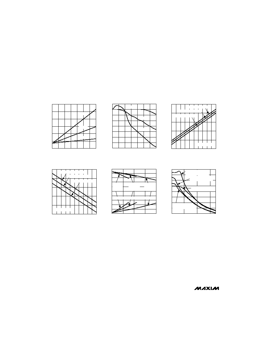
OH
)
vs. V
CC
POSITIVE SUPPLY VOLTAGE
V
OH
(V)
6.5
7.0
7.5
8.0
8.5
9.0
4.5
V
CC
(V)
MAX214-03
4.6 4.7 4.8 4.9 5.0 5.1 5.2 5.3 5.4 5.5
1 TRANSMITTER LOADED
2 TRANSMITTERS LOADED
3 TRANSMITTERS LOADED
DATA RATE = 0kbps
TRANSMITTER OUTPUT VOLTAGE (V
OH
)
vs. LOAD CAPACITANCE
AT DIFFERENT DATA RATES
V
OH
(V)
6.0
0
LOAD CAPACITANCE (pF)
MAX214-02
6.2
6.4
6.6
6.8
7.0
7.2
7.4
7.6
1000 2000 3000 4000 5000 6000 7000
20kbps
64kbps
120kbps
TRANSMITTER OUTPUT VOLTAGE (V
OL
)
vs. LOAD CAPACITANCE
AT DIFFERENT DATA RATES
V
OL
(V)
-8.5
-8.0
-7.5
-7.0
-6.5
-6.0
0
1000 2000 3000 4000 5000 6000 7000
LOAD CAPACITANCE (pF)
-5.5
MAX214-01
120kbps
64kbps
20kbps
MAX214
Programmable DTE/DCE,
+5V RS-232 Transceiver
4
_______________________________________________________________________________________
__________________________________________Typical Operating Characteristics
(V
CC
= 5V, C1 to C4 = 1
µ
F, all transmitters loaded with 3k
in parallel with 2.5nF, T
A
= +25°C, unless otherwise noted.)
TRANSMITTER OUTPUT VOLTAGE (V
OL)
vs. POSITIVE SUPPLY VOLTAGE
V
OL
(V)
-9.5
-9.0
-8.5
-8.0
-7.5
-7.0
4.5
V
CC
(V)
MAX214-04
4.6 4.7 4.8 4.9 5.0 5.1 5.2 5.3 5.4 5.5
3 TRANSMITTERS LOADED
2 TRANSMITTERS LOADED
1 TRANSMITTER LOADED
DATA RATE = 0kbps
TRANSMITTER OUTPUT VOLTAGES
vs. V+, V- LOAD CURRENT
T
OUT
+,
T
OUT
-
(V)
-10
0
LOAD CURRENT (mA)
MAX214-05
20
40
60
80
-8
-6
-4
-2
0
2
4
6
8
10
V+ AND V-
EQUALLY
LOADED
V+ LOADED,
NO LOAD
ON V-
V- LOADED,
NO LOAD
ON V+
ALL TRANSMITTERS UNLOADED, 0kbps
SLEW RATE vs. LOAD CAPACITANCE
SLEW RATE (V/
µ
s)
4
0
LOAD CAPACITANCE (pF)
MAX214-06
2000
4000
6000
6
8
10
12
14
16
18
20
SLEW+
3 TRANSMITTERS LOADED
SLEW-
3 TRANSMITTERS LOADED
SLEW+
1 TRANSMITTER LOADED
SLEW-
1 TRANSMITTER LOADED

_______________Detailed Description
The MAX214 RS-232 transceiver provides a complete,
8-line, software-configurable, DTE or DCE port RS-232
interface. Tx, Rx, RTS, CTS, DTR, DSR, DCD, and RI
circuits can be configured as either Data Terminal
Equipment (DTE) or Data Circuit-Terminating
Equipment (DCE) using the DTE/DCE control pin. The
MAX214 eliminates the need to swap cables when
switching between DTE and DCE configurations. This
is useful when, for example, a portable computer is
required to communicate with printers, modems, and
other computers without carrying multiple cables.
The MAX214 runs from a single +5V supply and incor-
porates a dual charge-pump voltage converter to gener-
ate the necessary voltages for the RS-232 transmitters.
A shutdown mode is provided to save power when
transmission is not required, but the receivers always
stay active for simple detection of ring indicator signals.
DTE/DCE Operation
The DTE/DCE pin allows circuit configuration under
software control. Tables 1a and 1b show the pin defini-
tions of the MAX214 in both DTE and DCE modes. The
Function columns show the direction of data flow from
the input pin to the output pin of the MAX214, and onto
the corresponding DB-25 connector's pin.
+5V to ±10V Dual Charge-Pump
Voltage Converter
The +5V to ±10V conversion is performed by two
charge-pump voltage converters (Figure 2). The first
uses capacitor C1 to double the +5V to +10V, storing
the +10V on the output filter capacitor, C3. The second
charge-pump voltage converter uses C2 to invert the
+10V to -10V, storing the -10V on the V- output filter
capacitor, C4.
In shutdown mode, V+ is pulled to V
CC
by an internal
resistor, and V- falls to GND.
MAX214
Programmable DTE/DCE,
+5V RS-232 Transceiver
_______________________________________________________________________________________
5
PIN
14
NAME
V-
9, 18, 20
TRA, TRC, TRB
15
V+
7
RDC
6, 8, 22, 23
RA, RE, RC, RB
5, 24, 25
TA, TC, TB
16
10, 17, 19
RTA, RTC, RTB
11
RDTC
V
CC
21
12
DTE/DCE
RRE
13
GND
26
SHDN
27, 28
3
C1+, C1-
1, 2
C2+, C2-
HI-Z
4
N.C.
FUNCTION
-2V
CC
voltage generated by the charge pump
+2V
CC
voltage generated by the charge pump
TTL/CMOS receiver A, E, C, B outputs
TTL/CMOS driver A, C, B inputs
+4.5V to +5.5V supply voltage
RS-232 receiver input
Ground
Shutdown control; shutdown high, normal operation low
Terminals for positive charge-pump capacitor
Terminals for negative charge-pump capacitor
No connect--not internally connected
______________________________________________________________Pin Description
RS-232 receiver impedance control. Take high to disconnect the termination resistor.
TTL/CMOS DTE receiver output D for DTE/DCE = 0V, or TTL/CMOS DCE receiver output C for
DTE/DCE = +5V
RS-232 DTE receiver input for DTE/DCE = 0V, or RS-232 DCE driver output for DTE/DCE = +5V
RS-232 DTE receiver input D for DTE/DCE = 0V, or RS-232 DCE driver output C for
DTE/DCE = +5V
Data terminal equipment (DTE) and data circuit-terminating equipment (DCE) control pin.
DCE active high and DTE active low.
RS-232 DTE driver output for DTE/DCE= 0V, or RS-232 DCE receiver input for DTE/DCE = +5V