Äîêóìåíòàöèÿ è îïèñàíèÿ www.docs.chipfind.ru
General Description
The MAX2055 high-performance, digitally controlled,
variable-gain, differential analog-to-digital converter
(ADC) driver/amplifier (DVGA) is designed for use from
30MHz to 300MHz in base station receivers.
The device integrates a digitally controlled attenuator
and a high-linearity single-ended-to-differential output
amplifier, which can either eliminate an external trans-
former, or can improve the even-order distortion perfor-
mance of a transformer-coupled circuit, thus relaxing
the requirements of the anti-alias filter preceding an
ADC. Targeted for ADC driver applications to adjust
gain either dynamically or as a one-time channel gain
setting, the MAX2055 is ideal for applications requiring
high performance. The attenuator provides 23dB of
attenuation range with ±0.2dB accuracy.
The MAX2055 is available in a thermally enhanced 20-
pin TSSOP-EP package and operates over the -40°C to
+85°C temperature range.
Applications
Cellular Base Stations
PHS/PAS Infrastructure
Receiver Gain Control
Broadband Systems
Automatic Test Equipment
Terrestrial Links
High-Performance ADC Drivers
Features
o 30MHz to 300MHz Frequency Range
o Single-Ended-to-Differential Conversion
o -3dB to +20dB Variable Gain
o 40dBm Output IP3 (at All Gain States and 70MHz)
o 2nd Harmonic -76dBc
o 3rd Harmonic -69dBc
o Noise Figure: 5.8dB at Maximum Gain
o Digitally Controlled Gain with 1dB Resolution and
±0.2dB Accuracy
o Adjustable Bias Current
MAX2055
Digitally Controlled, Variable-Gain, Differential
ADC Driver/Amplifier
________________________________________________________________ Maxim Integrated Products
1
Ordering Information
20
19
18
17
16
15
14
13
1
2
3
4
5
6
7
8
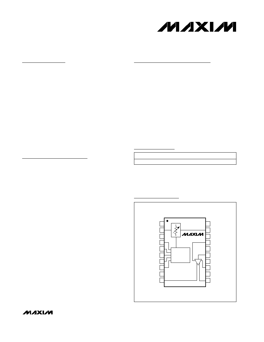
GND
ATTN
OUT
GND
I
SET
B4
GND
RF_IN
V
CC
C
C
AMP
IN
L
E
C
BP
B0
B1
B2
B3
12
11
9
10
I
BIAS
RF_OUT+
RF_OUT-
ATTENUATION
LOGIC
CONTROL
V
CC
TSSOP
MAX2055
TOP VIEW
19-2799; Rev 0; 4/03
For pricing, delivery, and ordering information, please contact Maxim/Dallas Direct! at
1-888-629-4642, or visit Maxim's website at www.maxim-ic.com.
PART
TEMP RANGE
PIN-PACKAGE
MAX2055EUP-T
-40
°C to +85°C
20 TSSOP-EP*
*EP = Exposed paddle.
Pin Configuration/
Functional Diagram
MAX2055
Digitally Controlled, Variable-Gain, Differential
ADC Driver/Amplifier
2
_______________________________________________________________________________________
ABSOLUTE MAXIMUM RATINGS
DC ELECTRICAL CHARACTERISTICS
(Circuit of Figure 1; V
CC
= +4.75V to +5.25V, GND = 0V. No input signals applied, and input and output ports are terminated with
50
. R1 = 1.13k, T
A
= -40°C to +85°C. Typical values are at V
CC
= +5V and T
A
= +25°C, unless otherwise noted.) (Notes 1, 2)
Stresses beyond those listed under "Absolute Maximum Ratings" may cause permanent damage to the device. These are stress ratings only, and functional
operation of the device at these or any other conditions beyond those indicated in the operational sections of the specifications is not implied. Exposure to
absolute maximum rating conditions for extended periods may affect device reliability.
All Pins to GND. .....................................-0.3V to +(V
CC
+ 0.25V)
Input Signal (RF_IN).....................................................20dBm
Output Power (RF_OUT) ...................................................24dBm
Continuous Power Dissipation (T
A
= +70°C)
20-Pin TSSOP (derate 21.7mW/°C above +70°C) ...........2.1W
Operating Temperature Range ...........................-40°C to +85°C
Junction Temperature ......................................................+150°C
Storage Temperature Range .............................-65°C to +165°C
Lead Temperature (soldering, 10s) .................................+300°C
PARAMETER
SYMBOL
CONDITIONS
MIN
TYP
MAX
UNITS
SUPPLY
Supply Voltage
V
CC
4.75
5.0
5.25
V
Supply Current
I
CC
240
290
mA
I
SET
Current
I
SET
1.1
mA
CONTROL INPUTS
Control Bits
Parallel
5
Bits
Input Logic High
2
V
Input Logic Low
0.6
V
Input Leakage Current
-1.2
+1.2
µA
PARAMETER
SYMBOL
CONDITIONS
MIN
TYP
MAX
UNITS
Frequency Range
f
R
30
300
MHz
Gain
G
19.9
dB
Amplitude Unbalance
(Note 3)
0.06
dB
Phase Unbalance
(Note 3)
0.7
D eg r ees
Minimum Reverse Isolation
29
dB
Noise Figure
NF
5.8
dB
Output 1dB Compression Point
P
1dB
25.7
dBm
2nd-Order Output Intercept Point
OIP2
f
1
+ f
2
, f
1
= 70MHz, f
2
= 71MHz, 5dBm/tone
at RF_OUT
75
dBm
3rd-Order Output Intercept Point
OIP3
All gain conditions, 5dBm/tone at RF_OUT
40
dBm
2nd Harmonic
2f
IN
-76
dBc
3rd Harmonic
3f
IN
-69
dBc
RF Gain-Control Range
23
dB
Gain-Control Resolution
1
dB
Attenuation Absolute Accuracy
Compared to the ideal expected attenuation
±0.2
dB
Attenuation Relative Accuracy
Between adjacent states
+0.05/
-0.2
dB
Gain Drift Over Temperature
T
A
= -40°C to +85°C
±0.3
dB
AC ELECTRICAL CHARACTERISTICS
(Circuit of Figure 1; V
CC
= +4.75V to +5.25V, GND = 0V, max gain (B0 = B1 = B2 = B3 = B4 = 0), R
1
= 1.13k
, P
OUT
= 5dBm,
f
IN
= 70MHz, 50
system impedance. Typical values are at V
CC
= +5V and T
A
= +25°C, unless otherwise noted.) (Notes 1, 2)
MAX2055
Digitally Controlled, Variable-Gain, Differential
ADC Driver/Amplifier
_______________________________________________________________________________________
3
Note 1: Guaranteed by design and characterization.
Note 2: All limits reflect losses of external components. Output measurements are taken at RF_OUT using the application circuit
shown in Figure 1.
Note 3: The amplitude and phase unbalance are tested with 50
resistors connected from OUT+/OUT- to GND.
PARAMETER
SYMBOL
CONDITIONS
MIN
TYP
MAX
UNITS
Gain Flatness Over 50MHz
Bandwidth
Peak-to-peak for all settings
0.5
dB
Attenuator Switching Time
50% control to 90% RF
40
ns
Input Return Loss
f
R
= 30MHz to 300MHz, all gain conditions
15
dB
f
R
= 30MHz to 250MHz, all gain conditions
15
Output Return Loss
f
R
= 250MHz to 300MHz, all gain conditions
12
dB
AC ELECTRICAL CHARACTERISTICS (continued)
(Circuit of Figure 1; V
CC
= +4.75V to +5.25V, GND = 0V, max gain (B0 = B1 = B2 = B3 = B4 = 0), R
1
= 1.13k
, P
OUT
= 5dBm,
f
IN
= 70MHz, 50
system impedance. Typical values are at V
CC
= +5V and T
A
= +25°C, unless otherwise noted.) (Notes 1, 2)
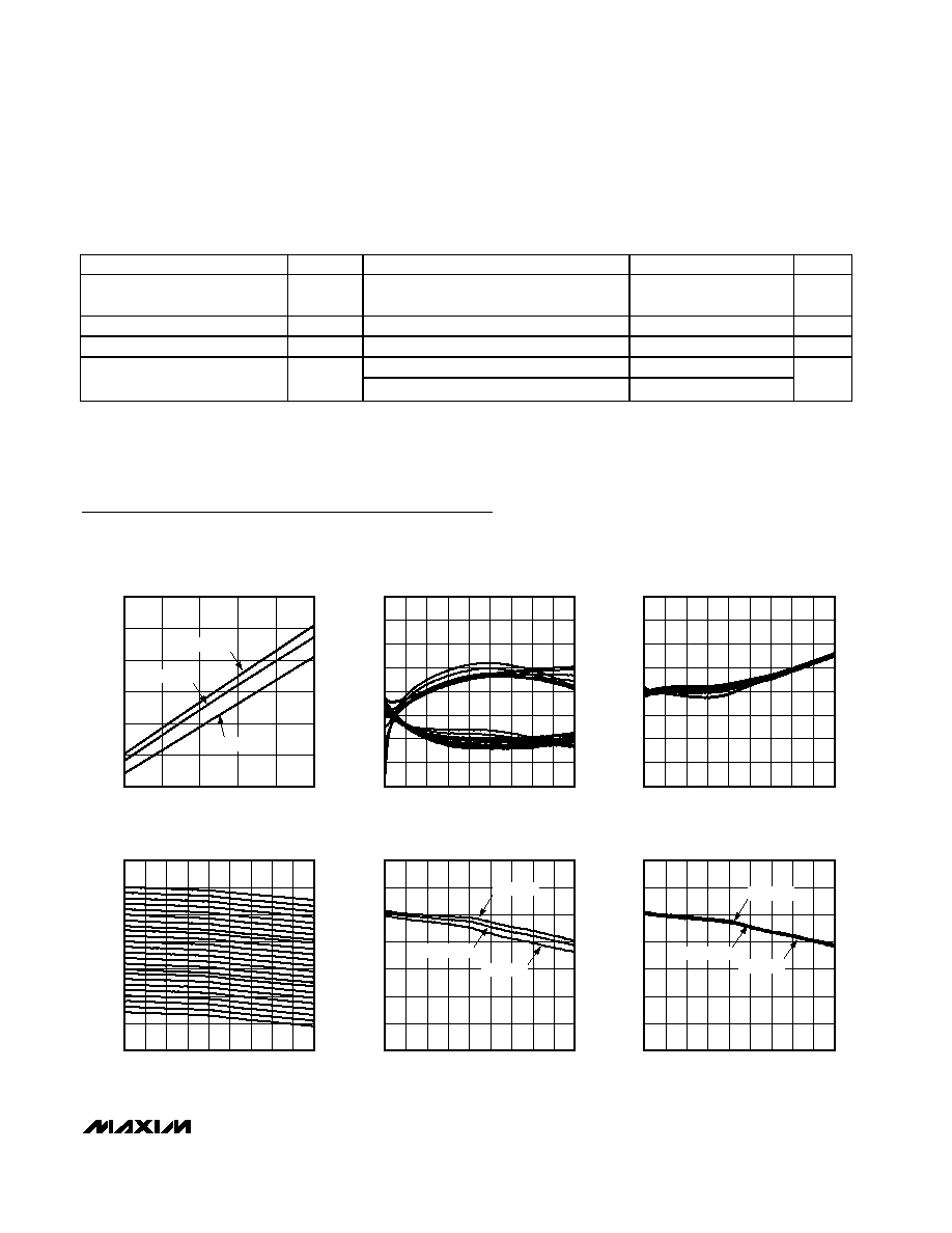
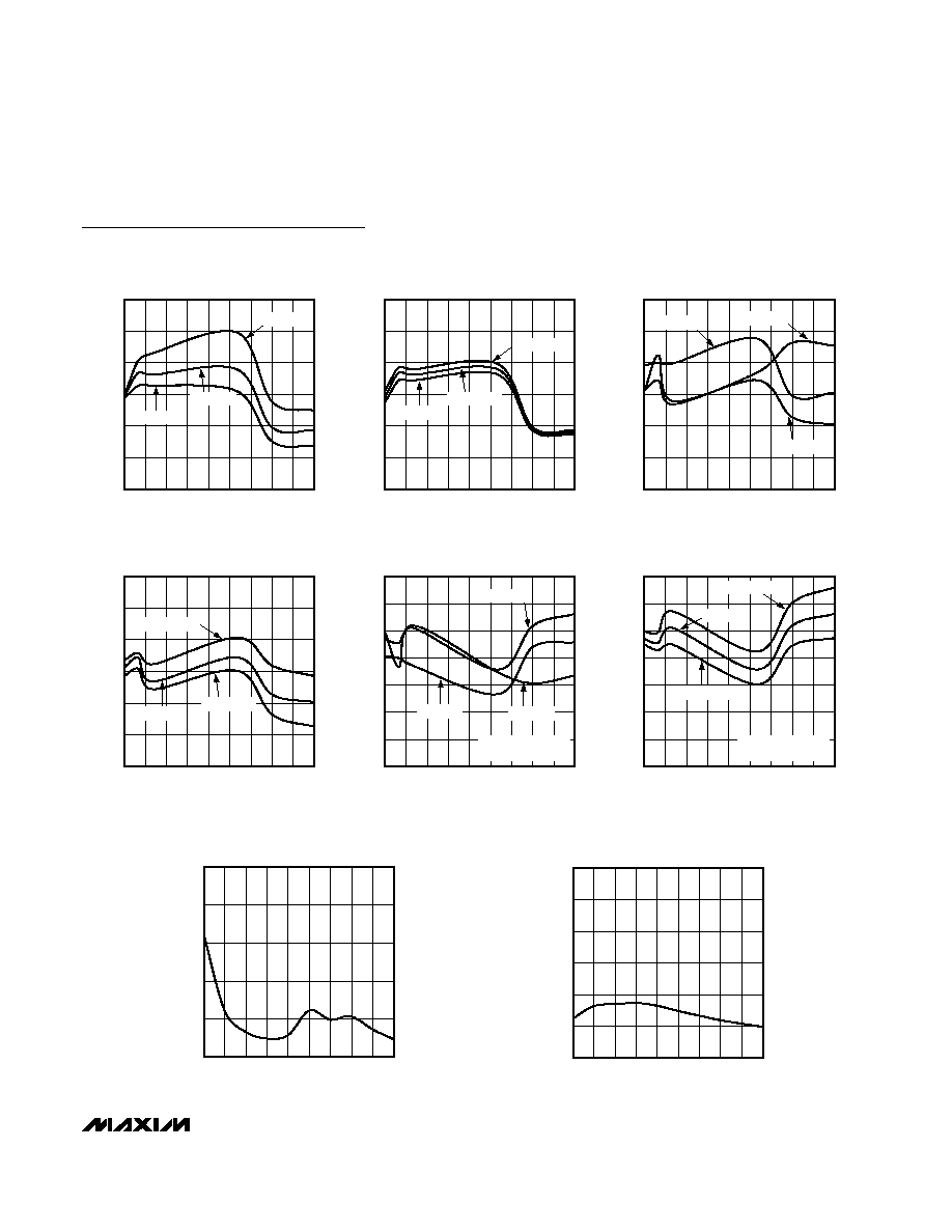
Typical Operating Characteristics
(Circuit of Figure 1, V
CC
= 5.0V, R
1
= 1.13k
, max gain (B0 = B1 = B2 = B3 = B4 = 0), P
OUT
= 5dBm, T
A
= +25°C, unless other-
wise noted.)
SUPPLY CURRENT vs. TEMPERATURE
MAX2055 toc01
TEMPERATURE (
°C)
SUPPLY CURRENT (mA)
60
35
10
-15
220
230
240
250
260
270
210
-40
85
V
CC
= 5.25V
V
CC
= 5.0V
V
CC
= 4.75V
INPUT RETURN LOSS vs. RF FREQUENCY
(ALL STATES)
MAX2055 toc02
FREQUENCY (MHz)
INPUT RETURN LOSS (dB)
270
240
60
90 120
180
150
210
35
30
25
20
15
10
5
0
40
30
300
OUTPUT RETURN LOSS vs. RF FREQUENCY
(ALL STATES)
MAX2055 toc03
FREQUENCY (MHz)
OUTPUT RETURN LOSS (dB)
270
240
60
90 120
180
150
210
35
30
25
20
15
10
5
0
40
30
300
GAIN vs. RF FREQUENCY (ALL STATES)
MAX2055 toc04
FREQUENCY (MHz)
GAIN (dB)
270
240
60
90 120
180
150
210
-5
0
5
10
15
20
25
-10
30
300
GAIN vs. RF FREQUENCY
MAX2055 toc05
FREQUENCY (MHz)
GAIN (dB)
270
240
60
90 120
180
150
210
12
14
16
18
20
22
24
10
30
300
T
A
= +85
°C
T
A
= +25
°C
T
A
= -40
°C
GAIN vs. RF FREQUENCY
MAX2055 toc06
FREQUENCY (MHz)
GAIN (dB)
270
240
60
90 120
180
150
210
12
14
16
18
20
22
24
10
30
300
V
CC
= 5.25V
V
CC
= 5.0V
V
CC
= 4.75V
MAX2055
Digitally Controlled, Variable-Gain, Differential
ADC Driver/Amplifier
4
_______________________________________________________________________________________
ATTENUATION ABSOLUTE ACCURACY
(ALL STATES)
MAX2055 toc07
FREQUENCY (MHz)
ABSOLUTE ACCURACY (dB)
270
240
60
90 120
180
150
210
-0.8
-0.6
-0.4
-0.2
0
0.2
0.4
0.6
0.8
1.0
-1.0
30
300
ATTENUATION RELATIVE ACCURACY
(ALL STATES)
MAX2055 toc08
FREQUENCY (MHz)
RELATIVE ACCURACY (dB)
270
240
60
90 120
180
150
210
-0.8
-0.6
-0.4
-0.2
0
0.2
0.4
0.6
0.8
1.0
-1.0
30
300
REVERSE ISOLATION vs. RF FREQUENCY
MAX2055 toc09
FREQUENCY (MHz)
REVERSE ISOLATION (dB)
270
240
60
90 120
180
150
210
24
28
32
36
40
20
30
300
NOISE FIGURE vs. FREQUENCY
MAX2055 toc10
FREQUENCY (MHz)
NOISE FIGURE (dB)
270
240
60
90 120
180
150
210
4.5
5.0
5.5
6.0
6.5
7.0
7.5
8.0
4.0
30
300
T
A
= +85
°C
T
A
= -40
°C
T
A
= +25
°C
OUTPUT P-1dB vs. FREQUENCY
MAX2055 toc11
FREQUENCY (MHz)
OUTPUT P-1dB (dBm)
270
240
60
90 120
180
150
210
22
23
24
25
26
27
21
30
300
T
A
= +85
°C
T
A
= -40
°C
T
A
= +25
°C
OUTPUT P-1dB vs. FREQUENCY
MAX2055 toc12
FREQUENCY (MHz)
OUTPUT P-1dB (dBm)
270
240
60
90 120
180
150
210
22
23
24
25
26
27
21
30
300
V
CC
= +4.75V
V
CC
= +5V
V
CC
= +5.25V
OUTPUT IP3 vs. FREQUENCY
MAX2055 toc13
FREQUENCY (MHz)
OIP3 (dBm)
270
240
60
90 120
180
150
210
32
34
36
38
42
40
44
30
30
300
T
A
= +85
°C
T
A
= -40
°C
T
A
= +25
°C
P
RF1
= P
RF2
= 5dBm
AT OUTPUT,
f = 1MHz
OUTPUT IP3 vs. FREQUENCY
MAX2055 toc14
FREQUENCY (MHz)
OIP3 (dBm)
270
240
60
90 120
180
150
210
32
34
36
38
42
40
44
30
30
300
V
CC
= +5.25V
V
CC
= +4.75V
V
CC
= +5V
P
RF1
= P
RF2
= 5dBm
AT OUTPUT,
f = 1MHz
INPUT IP3 vs. ATTENUATION STATE
MAX2055 toc15
ATTENUATION STATE
IIP3 (dBm)
20
16
4
8
12
20
25
30
35
40
45
50
55
15
0
24
P
RF1
= P
RF2
= 5dBm
AT OUTPUT,
f = 1MHz,
f
IN
= 70MHz
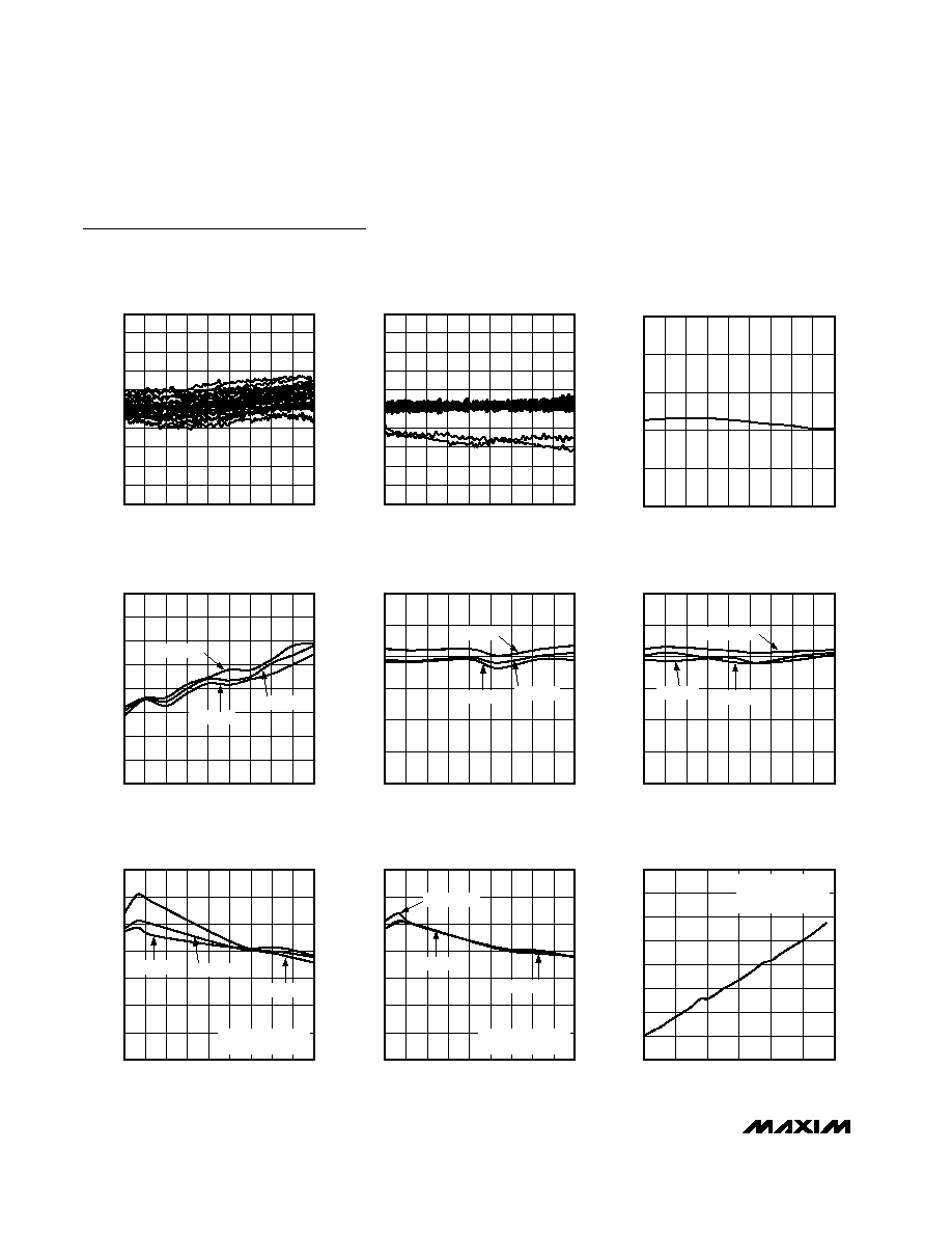
Typical Operating Characteristics (continued)
(Circuit of Figure 1, V
CC
= 5.0V, R
1
= 1.13k
, max gain (B0 = B1 = B2 = B3 = B4 = 0), P
OUT
= 5dBm, T
A
= +25°C, unless other-
wise noted.)
MAX2055
Digitally Controlled, Variable-Gain, Differential
ADC Driver/Amplifier
_______________________________________________________________________________________
5
3RD HARMONIC vs. FREQUENCY
MAX2055 toc16
FREQUENCY (MHz)
HARMONIC (dBc)
270
240
60
90 120
180
150
210
-80
-75
-70
-65
-60
-55
-85
30
300
T
A
= +85
°C
T
A
= -40
°C
T
A
= +25
°C
3RD HARMONIC vs. FREQUENCY
MAX2055 toc17
FREQUENCY (MHz)
HARMONIC (dBc)
270
240
60
90 120
180
150
210
-80
-75
-70
-65
-60
-55
-85
30
300
V
CC
= +5V
V
CC
= +5.25V
V
CC
= +4.75V
2ND HARMONIC vs. FREQUENCY
MAX2055 toc18
FREQUENCY (MHz)
HARMONIC (dBc)
270
240
60
90 120
180
150
210
-80
-75
-70
-65
-60
-85
-90
30
300
T
A
= +85
°C
T
A
= -40
°C
T
A
= +25
°C
2ND HARMONIC vs. FREQUENCY
MAX2055 toc19
FREQUENCY (MHz)
HARMONIC (dBc)
270
240
60
90 120
180
150
210
-80
-75
-70
-65
-60
-85
-90
30
300
V
CC
= +4.75V
V
CC
= +5.25V
V
CC
= +5V
OUTPUT IP2 vs. FREQUENCY (f
1
+ f
2
)
MAX2055 toc20
FREQUENCY (MHz)
OIP2 (dBm)
270
240
60
90 120
180
150
210
55
60
65
70
80
75
85
50
30
300
T
A
= +85
°C
T
A
= -40
°C
T
A
= +25
°C
P
RF1
= P
RF2
= 5dBm
AT OUTPUT,
f = 1MHz
OUTPUT IP2 vs. FREQUENCY (f
1
+ f
2
)
MAX2055 toc21
FREQUENCY (MHz)
OIP2 (dBm)
270
240
60
90 120
180
150
210
55
60
65
70
80
75
85
50
30
300
V
CC
= +5.25V
V
CC
= +4.75V
V
CC
= +5.0
P
RF1
= P
RF2
= 5dBm
AT OUTPUT,
f = 1MHz
OUTPUT-PORT AMPLITUDE UNBALANCE
vs. FREQUENCY
MAX2055 toc22
FREQUENCY (MHz)
AMPLITUDE UNBALANCE (dB)
270
240
60
90 120
180
150
210
0.05
0.10
0.15
0.20
0.25
0
30
300
OUTPUT-PORT PHASE UNBALANCE
vs. FREQUENCY
MAX2055 toc23
FREQUENCY (MHz)
PHASE UNBALANCE (DEGREES)
270
240
60
90 120
180
150
210
0.5
1.0
1.5
2.0
2.5
3.0
0
30
300
Typical Operating Characteristics (continued)
(Circuit of Figure 1, V
CC
= 5.0V, R
1
= 1.13k
, max gain (B0 = B1 = B2 = B3 = B4 = 0), P
OUT
= 5dBm, T
A
= +25°C, unless other-
wise noted.)