Äîêóìåíòàöèÿ è îïèñàíèÿ www.docs.chipfind.ru
General Description
The MAX2009 adjustable RF predistorter is designed to
improve power amplifier (PA) adjacent-channel power
rejection (ACPR) by introducing gain and phase expan-
sion in a PA chain to compensate for the PA's gain and
phase compression. With its +23dBm maximum input
power level and wide adjustable range, the MAX2009
can provide up to 12dB of ACPR improvement for
power amplifiers operating in the 1200MHz to 2500MHz
frequency band. Lower frequencies of operation can be
achieved with this IC's counterpart, the MAX2010.
The MAX2009 is unique in that it provides up to 7dB of
gain expansion and 24° of phase expansion as the
input power is increased. The amount of expansion is
configurable through two independent sets of control:
one set adjusts the gain expansion breakpoint
and slope, while the second set controls the same
parameters for phase. With these settings in place, the
linearization circuit can be run in either a static set-and-
forget mode, or a more sophisticated closed-loop
implementation can be employed with real-time soft-
ware-controlled distortion correction. Hybrid correction
modes are also possible using simple lookup tables to
compensate for factors such as PA temperature drift
or PA loading.
The MAX2009 comes in a 28-pin thin QFN exposed
pad (EP) package (5mm x 5mm) and is specified for
the extended (-40°C to +85°C) temperature range.
Applications
WCDMA/UMTS, cdma2000, DCS1800, and
PCS1900 Base Stations
Feed-Forward PA Architectures
Digital Baseband Predistortion Architectures
Military Applications
WLAN Applications
Features
o Up to 12dB ACPR Improvement*
o Independent Gain and Phase Expansion Controls
o Gain Expansion Up to 7dB
o Phase Expansion Up to 24°
o 1200MHz to 2500MHz Frequency Range
o Exceptional Gain and Phase Flatness
o Group Delay <1.3ns (Gain and Phase Sections
Combined)
o ±0.04ns Group Delay Ripple Over a 100MHz Band
o Capable of Handling Input Drives Up to +23dBm
o On-Chip Temperature Variation Compensation
o Single +5V Supply
o Low Power Consumption: 75mW (typ)
o Fully Integrated into Small 28-Pin Thin QFN
Package
*Performance dependent on amplifier, bias, and modulation.
MAX2009
1200MHz to 2500MHz Adjustable
RF Predistorter
________________________________________________________________ Maxim Integrated Products
1
28
27
26
25
24
23
22
7
6
5
4
3
2
1
15
16
17
18
19
20
21
8
9
10
11
12
13
14
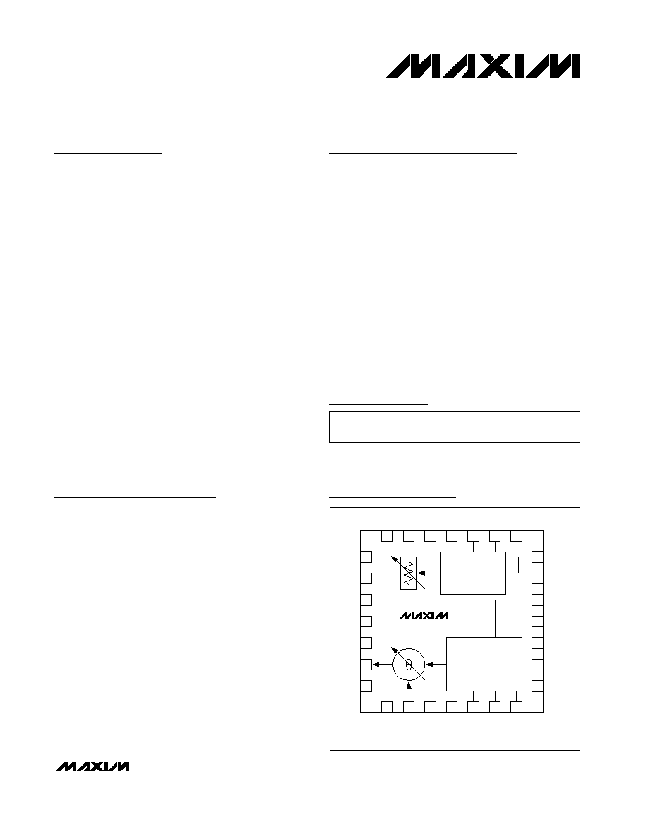
MAX2009
GAIN
CONTROL
PHASE
CONTROL
GND*
GND*
ING
GND*
GND*
OUTP
GND*
V
CCG
GND*
PBRAW
PBEXP
PBIN
GND*
V
CCP
GND*
INP
GND*
PFS1
PFS2
PDCS1
PDCS2
GND*
OUTG
GND*
GCS
GFS
GBP
GND*
*INTERNALLY CONNECTED TO EXPOSED GROUND PADDLE.
Functional Diagram/
Pin Configuration
Ordering Information
19-2929; Rev 0; 8/03
For pricing, delivery, and ordering information, please contact Maxim/Dallas Direct! at
1-888-629-4642, or visit Maxim's website at www.maxim-ic.com.
*EP = Exposed paddle.
PART
TEMP RANGE
PIN-PACKAGE
MAX2009ETI-T
-40
°C to +85°C
28 Thin QFN-EP*
MAX2009
1200MHz to 2500MHz Adjustable
RF Predistorter
2
_______________________________________________________________________________________
ABSOLUTE MAXIMUM RATINGS
DC ELECTRICAL CHARACTERISTICS
(MAX2009 EV kit; V
CCG
= V
CCP
= +4.75V to +5.25V; no RF signal applied; INP, ING, OUTP, OUTG are AC-coupled and terminated to
50
; V
PF_S1
= open; PBEXP shorted to PBRAW; V
PDCS1
= V
PDCS2
= 0.8V; V
PBIN
= V
GBP
= V
GCS
= GND; V
GFS
= V
CCG
; T
A
= -40
°C to
+85
°C. Typical values are at V
CCG
= V
CCP
= +5.0V, T
A
= +25
°C, unless otherwise noted.)
Stresses beyond those listed under "Absolute Maximum Ratings" may cause permanent damage to the device. These are stress ratings only, and functional
operation of the device at these or any other conditions beyond those indicated in the operational sections of the specifications is not implied. Exposure to
absolute maximum rating conditions for extended periods may affect device reliability.
V
CCG
, V
CCP
to GND ..............................................-0.3V to +5.5V
ING, OUTG, GCS, GFS, GBP to GND......-0.3V to (V
CCG
+ 0.3V)
INP, OUTP, PFS_, PDCS_, PBRAW,
PBEXP, PBIN to GND ............................-0.3V to (V
CCP
+ 0.3V)
Input (ING, INP, OUTP, OUTG) Level ............................+23dBm
PBEXP Output Current ........................................................
±1mA
Continuous Power Dissipation (T
A
= +70
°C)
28-Pin Thin QFN-EP
(derate 21mW/
°C above +70°C)...............................1667mW
Operating Temperature Range ...........................-40
°C to +85°C
Junction Temperature ......................................................+150
°C
Storage Temperature Range .............................-65
°C to +150°C
Lead Temperature (soldering 10s) ..................................+300
°C
PARAMETER
CONDITIONS
MIN
TYP
MAX
UNITS
Supply Voltage
V
CCG
, V
CCP
4.75
5.25
V
V
CCP
5.8
7
Supply Current
V
CCG
10
12.1
mA
PBIN, PBRAW
0
V
CCP
Analog Input Voltage Range
GBP, GFS, GCS
0
V
CCG
V
V
GFS
= V
GCS
= V
PBRAW
= 0V
-2
+2
V
GBP
= 0 to +5V
-100
+170
Analog Input Current
V
PBIN
= 0 to +5V
-100
+220
µA
Logic-Input High Voltage
PDCS1, PDCS2 (Note 1)
2.0
V
Logic-Input Low Voltage
PDCS1, PDCS2 (Note 1)
0.8
V
Logic Input Current
-2
+2
µA
MAX2009
1200MHz to 2500MHz Adjustable
RF Predistorter
_______________________________________________________________________________________
3
AC ELECTRICAL CHARACTERISTICS
(MAX2009 EV kit, V
CCG
= V
CCP
= +4.75V to +5.25V, 50
environment, P
IN
= -20dBm, f
IN
= 1200MHz to 2500MHz, V
GCS
= +1.0V,
V
GFS
= +5.0V, V
GBP
= +1.2V, V
PBIN
= V
PDCS1
= V
PDCS2
= 0V, V
PF_S1
= +5V, V
PBRAW
= V
PBEXP
, T
A
= -40
°C to +85°C. Typical values
are at f
IN
= 2140MHz, V
CCG
= V
CCP
= +5V, T
A
= +25
°C, unless otherwise noted.) (Notes 1, 2)
PARAMETER
CONDITIONS
MIN
TYP
MAX
UNITS
Operating Frequency Range
1200
2500
MHz
VSWR
ING, INP, OUTG, OUTP
1.3:1
PHASE CONTROL SECTION
Nominal Gain
-7.5
dB
Gain Variation Over Temperature
T
A
= -40
°C to +85°C
-1.4
dB
Gain Flatness
Over a 100MHz band
±0.1
dB
Phase-Expansion Breakpoint
Maximum
V
PBIN
= +5V
23
dBm
Phase-Expansion Breakpoint
Minimum
V
PBIN
= 0V
3.7
dBm
Phase-Expansion Breakpoint
Variation Over Temperature
T
A
= -40
°C to +85°C
±1.3
dB
V
PF_S1
= +5V, V
PDCS1
= V
PDCS2
= 0V,
P
IN
= -20 dBm to +23 dBm
23.7
V
PDCS1
= 5V, V
PDCS2
= 0V, V
PF_S1
= +1.5V
14.2
V
PDCS1
= 0V, V
PDCS2
= 5V, V
PF_S1
= +1.5V
9.2
Phase Expansion
V
PF_S1
= 0V, V
PDCS1
= V
PDCS2
= +5V,
P
IN
= -20dBm to +23dBm
7.6
Degrees
Phase-Expansion Slope
Maximum
P
IN
= +15dBm
1.2
Degrees
/dB
Phase-Expansion Slope Minimum
V
PF_S1
= 0V, V
PDCS1
= V
PDCS2
= +5V,
P
IN
= +15dBm
0.4
Degrees
/dB
Phase Slope Variation Over
Temperature
P
IN
= +15dBm, T
A
= -40°C to +85°C
-0.1
Degrees
/dB
Phase Ripple
Over a 100MHz band, deviation from linear phase
±0.15
Degrees
Noise Figure
7.5
dB
Absolute Group Delay
Interconnects de-embedded
0.7
ns
Group Delay Ripple
Over a 100MHz band
±0.03
ns
Parasitic Gain Expansion
P
IN
= -20dBm to +23dBm
0.9
dB
MAX2009
1200MHz to 2500MHz Adjustable
RF Predistorter
4
_______________________________________________________________________________________
Note 1: Guaranteed by design and characterization.
Note 2: All limits reflect losses and characteristics of external components shown in the Typical Application Circuit, unless otherwise
noted.
AC ELECTRICAL CHARACTERISTICS (continued)
(MAX2009 EV kit, V
CCG
= V
CCP
= +4.75V to +5.25V, 50
environment, P
IN
= -20dBm, f
IN
= 1200MHz to 2500MHz, V
GCS
= +1.0V,
V
GFS
= +5.0V, V
GBP
= +1.2V, V
PBIN
= V
PDCS1
= V
PDCS2
= 0V, V
PF_S1
= +5V, V
PBRAW
= V
PBEXP
, T
A
= -40
°C to +85°C. Typical values
are at f
IN
= 2140MHz, V
CCG
= V
CCP
= +5V, T
A
= +25
°C, unless otherwise noted.) (Notes 1, 2)
PARAMETER
CONDITIONS
MIN
TYP
MAX
UNITS
GAIN CONTROL SECTION
-16
V
GCS
= 0V, V
GFS
= +5V
-23
Nominal Gain
V
GCS
= +5V, V
GFS
= 0V
-8.5
dB
Gain Variation Over Temperature
T
A
= -40
°C to +85°C
-1
dB
Gain Flatness
Over a 100MHz band
±0.3
dB
Gain-Expansion Breakpoint
Maximum
V
GBP
= +5V
23
dBm
Gain-Expansion Breakpoint
Minimum
V
GBP
= +0.5V
-3
dBm
Gain-Expansion Breakpoint
Variation Over Temperature
T
A
= -40
°C to +85°C
-0.3
dB
V
GFS
= +5V, P
IN
= -20dBm to +23dBm
6.6
Gain Expansion
V
GFS
= 0V, P
IN
= -20dBm to +23dBm
3.6
dB
V
GFS
= +5V, P
IN
= +15dBm
0.5
Gain-Expansion Slope
V
GFS
= +0V, P
IN
= +15dBm
0.26
dB/dB
Gain Slope Variation Over
Temperature
P
IN
= +15dBm, T
A
= -40
°C to +85°C
-0.04
dB/dB
Noise Figure
16
dB
Absolute Group Delay
Interconnects de-embedded
0.61
ns
Group Delay Ripple
Over a 100MHz band
±0.01
ns
Phase Ripple
Over a 100MHz band, deviation from linear phase
±0.07
Degrees
Parasitic Phase Expansion
P
IN
= -20dBm to +23dBm
5
Degrees
MAX2009
1200MHz to 2500MHz Adjustable
RF Predistorter
_______________________________________________________________________________________
5
5.3
5.6
5.5
5.4
5.7
5.8
5.9
6.0
6.1
6.2
6.3
4.75
4.95
4.85
5.05
5.15
5.25
SUPPLY CURRENT
vs. SUPPLY VOLTAGE
MAX2009TOC01
SUPPLY VOLTAGE (V)
SUPPLY CURRENT (mA)
T
A
= +85
°C
T
A
= +25
°C
T
A
= -40
°C
SMALL-SIGNAL INPUT RETURN LOSS
vs. FREQUENCY
MAX2009TOC02
40
35
25
30
10
5
15
20
0
INPUT RETURN LOSS (dB)
1.1
1.5
1.7
1.3
1.9
2.1
2.3
2.5
FREQUENCY (GHz)
A = V
PDCS1
= V
PDCS2
= V
PF_S1
= 0V
B = V
PDCS1
= V
PDCS2
= 0V, V
PF_S1
= 5V
C = V
PDCS1
= V
PDCS2
= 5V, V
PF_S1
= 0V
D = V
PDCS1
= V
PDCS2
= V
PF_S1
= 5V
B
D
C
A
SMALL-SIGNAL OUTPUT RETURN LOSS
vs. FREQUENCY
MAX2009TOC03
40
35
25
30
10
5
15
20
0
OUTPUT RETURN LOSS (dB)
1.1
1.5
1.7
1.3
1.9
2.1
2.3
2.5
FREQUENCY (GHz)
A = V
PDCS1
= V
PDCS2
= V
PF_S1
= 0V
B = V
PDCS1
= V
PDCS2
= 0V, V
PF_S1
= 5V
C = V
PDCS1
= V
PDCS2
= 5V, V
PF_S1
= 0V
D = V
PDCS1
= V
PDCS2
= V
PF_S1
= 5V
B
C
A
D
LARGE-SIGNAL INPUT RETURN LOSS
vs. FREQUENCY
MAX2009TOC04
40
35
25
30
10
5
15
20
0
INPUT RETURN LOSS (dB)
1.1
1.5
1.7
1.3
1.9
2.1
2.3
2.5
FREQUENCY (GHz)
A = V
PDCS1
= V
PDCS2
= V
PF_S1
= 0V
B = V
PDCS1
= V
PDCS2
= 0V, V
PF_S1
= 5V
C = V
PDCS1
= V
PDCS2
= 5V, V
PF_S1
= 0V
D = V
PDCS1
= V
PDCS2
= V
PF_S1
= 5V
C
D
B
A
P
IN
= +15dBm
LARGE-SIGNAL OUTPUT RETURN LOSS
vs. FREQUENCY
MAX2009TOC05
40
35
25
30
10
5
15
20
0
OUTPUT RETURN LOSS (dB)
1.1
1.5
1.7
1.3
1.9
2.1
2.3
2.5
FREQUENCY (GHz)
A = V
PDCS1
= V
PDCS2
= V
PF_S1
= 0V
B = V
PDCS1
= V
PDCS2
= 0V, V
PF_S1
= 5V
C = V
PDCS1
= V
PDCS2
= 5V, V
PF_S1
= 0V
D = V
PDCS1
= V
PDCS2
= V
PF_S1
= 5V
C
D
B
A
P
IN
= +15dBm
-10.0
-8.5
-9.0
-9.5
-7.5
-8.0
-5.5
-6.0
-6.5
-7.0
-5.0
1.1
1.3
1.5
1.7
1.9
2.1
2.3
2.5
SMALL-SIGNAL GAIN
vs. FREQUENCY
MAX2009TOC06
FREQUENCY (GHz)
GAIN (dB)
T
A
= +85
°C
T
A
= +25
°C
T
A
= -40
°C
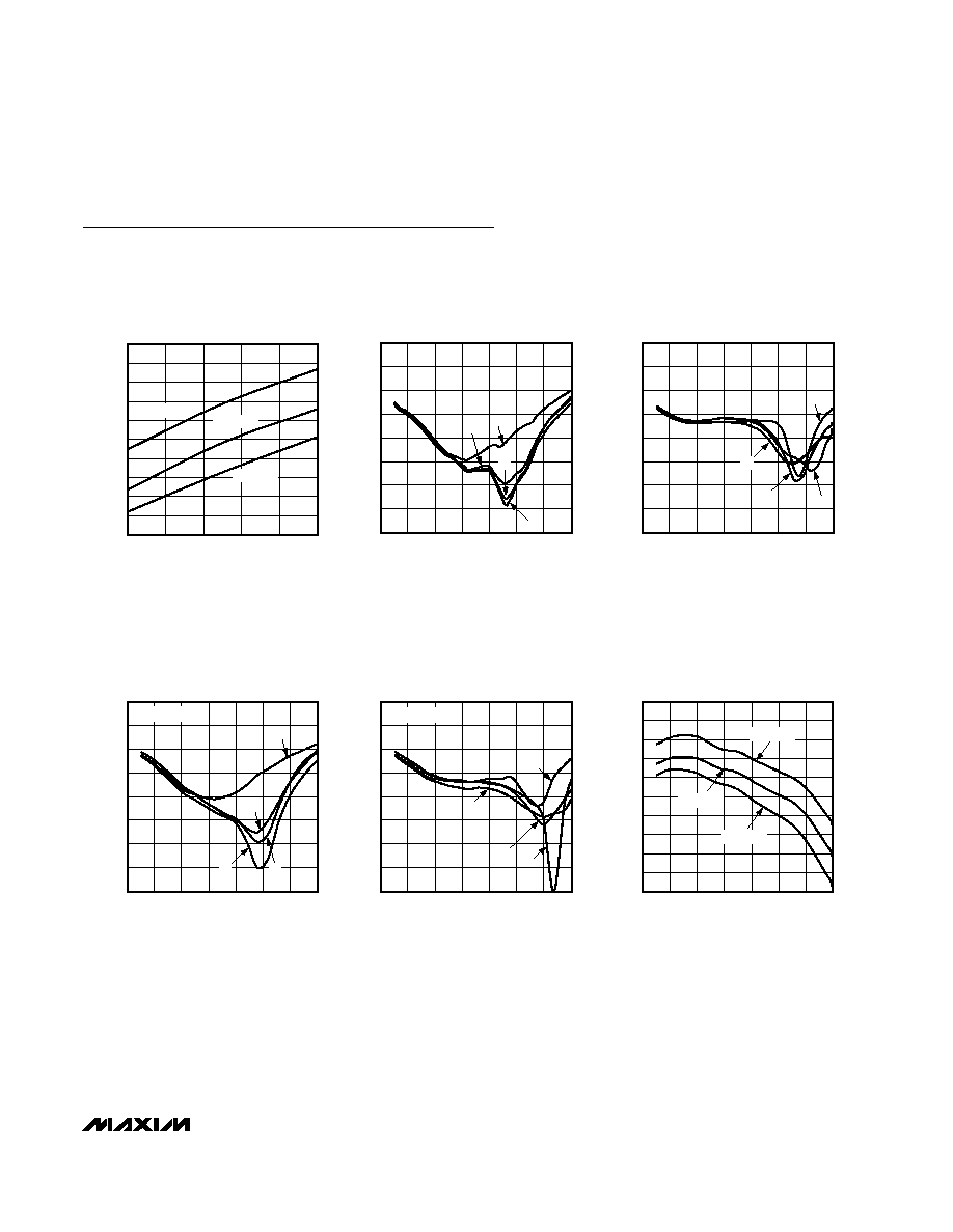
Typical Operating Characteristics
Phase Control Section
(MAX2009 EV kit, V
CCP
= +5.0V, P
IN
= -20dBm, V
PBIN
= 0V, V
PF_S1
= +5.0V, V
PDCS1
= V
PDCS2
= 0V, f
IN
= 2140MHz, T
A
= +25
°C,
unless otherwise noted.)