Äîêóìåíòàöèÿ è îïèñàíèÿ www.docs.chipfind.ru
General Description
The MAX1997/MAX1998 provide the voltages required for
active-matrix, thin-film transistor liquid-crystal displays
(TFT LCDs). Both combine a high-performance step-up
regulator with two linear-regulator controllers, input pro-
tection switch control, and flexible sequence program-
ming. The MAX1997 contains two additional linear-
regulator controllers and a VCOM buffer. The MAX1997/
MAX1998 can operate from input supplies of 2.7V to 5.5V
and feature multiple levels of protection circuitry, making
them complete power-supply systems for displays.
The main DC-DC converter provides the regulated supply
voltage for the display's source-driver ICs. The converter
is a high-frequency (up to 1.5MHz) step-up regulator with
an integrated 14V N-channel MOSFET that allows the use
of ultra-small inductors and ceramic capacitors while
achieving efficiencies over 85%. Its current-mode control
architecture provides fast transient response to pulsed
loads. Internal soft-start and cycle-by-cycle current limit
help prevent input surge currents.
The positive and negative linear-regulator controllers
postregulate charge-pump outputs for TFT gate-on and
gate-off supplies. Both linear-regulator controllers, as well
as the step-up regulator, have supply-sequencing control
inputs. The three outputs can be sequenced in any order
by selecting the appropriate external components.
The MAX1997 features a high-current backplane driver
(VCOM). This buffer provides peak currents exceeding
300mA (typ) and requires only a 0.47µF output filter
capacitor. The MAX1997's two additional linear-regulator
controllers can be used to build the gamma reference
voltage and a logic supply.
The MAX1997/MAX1998 have a unique input switch con-
trol that can replace the typical input supply fuse. When a
fault is detected, the regulator is disconnected from the
input supply. The fault detector monitors all the regulated
output voltages and the current from the input supply. In
addition, the MAX1997/MAX1998 enter shutdown when
the internal over-temperature threshold is reached.
The MAX1997 is available in a 32-pin thin QFN package
and the MAX1998 is available in a 20-pin thin QFN pack-
age. Both packages have a maximum thickness of
0.8mm suitable for ultra-thin LCD panels.
Applications
Notebook Computer Displays
LCD Monitors
Car Navigation Displays
Features
o 2.7V to 5.5V Input Supply Range
o Adjustable (Up to +13V) Output Voltage for
Source-Driver ICs
o Integrated High-Efficiency Power MOSFET
o Linear-Regulator Controllers for TFT Gate-On and
Gate-Off Supplies
o High-Current VCOM Buffer (MAX1997 Only)
o Two Additional Linear-Regulator Controllers
(MAX1997 Only)
o Programmable Power-Up Sequencing
o Multiple Overload Protection with Thermal
Shutdown
o 1µA Shutdown Current
o 32-Pin/20-Pin Thin QFN Packages
MAX1997/MAX1998
Quintuple/Triple-Output TFT LCD Power Supplies
with Fault Protection and VCOM Buffer
________________________________________________________________ Maxim Integrated Products
1
19-2638; Rev 0; 10/02
For pricing, delivery, and ordering information, please contact Maxim/Dallas Direct! at
1-888-629-4642, or visit Maxim's website at www.maxim-ic.com.
Ordering Information
PART
TEMP RANGE
PIN-PACKAGE
MAX1997ETJ
-40
°C to +85°C 32 Thin QFN 5mm x 5mm
MAX1998ETP
-40
°C to +85°C 20 Thin QFN 5mm x 5mm
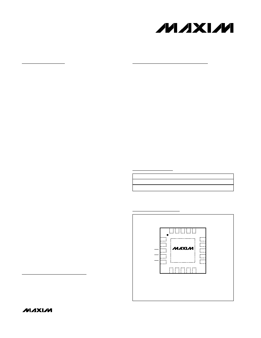
FREQ
IN
GATE
OCP
OCN
DRVN
FBN
DRVA
REF
GND
FB
FBP
DRVP
LX
ON2
ONP
ONN
CT
PGND
TGNDA
TOP VIEW
20
19
18
17
16
13
12
11
14
15
4
3
2
1
5
6
7
8
9
10
MAX1998
THIN QFN 5mm
× 5mm
Pin Configurations
Pin Configurations continued at end of data sheet.
MAX1997/MAX1998
Quintuple/Triple-Output TFT LCD Power Supplies
with Fault Protection and VCOM Buffer
2
_______________________________________________________________________________________
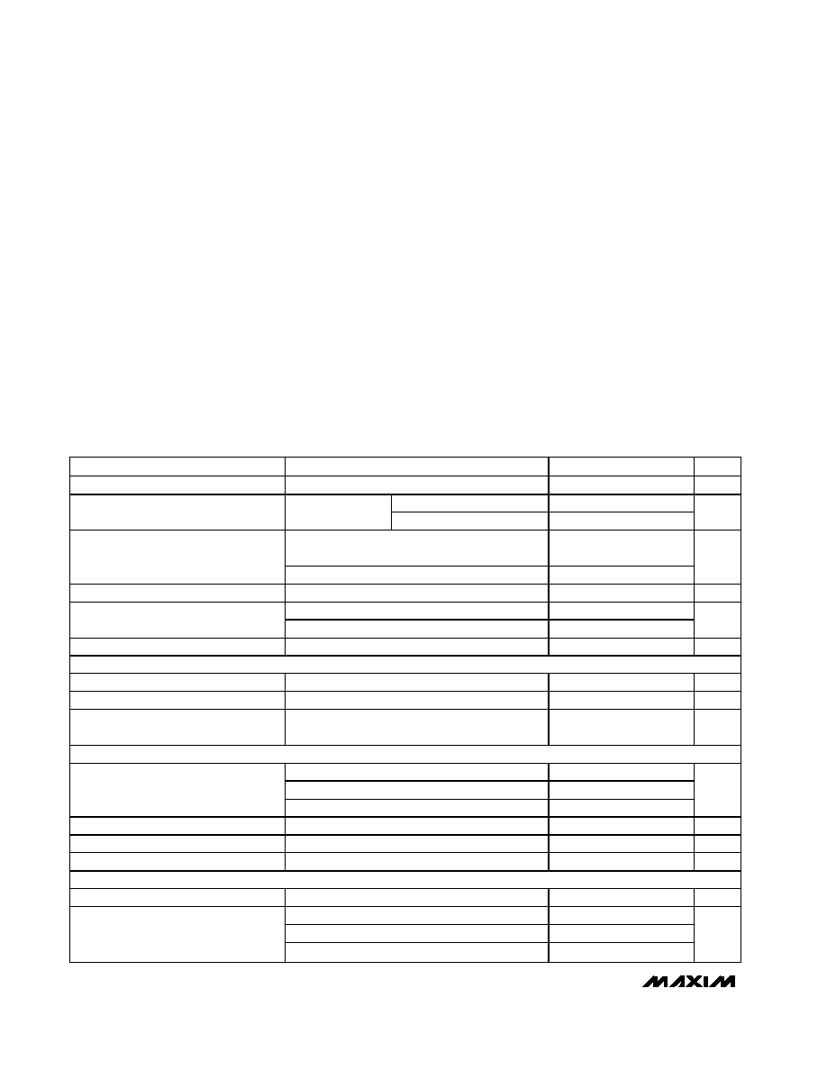
ABSOLUTE MAXIMUM RATINGS
Stresses beyond those listed under "Absolute Maximum Ratings" may cause permanent damage to the device. These are stress ratings only, and functional
operation of the device at these or any other conditions beyond those indicated in the operational sections of the specifications is not implied. Exposure to
absolute maximum rating conditions for extended periods may affect device reliability.
IN, SHDN, FB, FBP, FBN, FB1, FB2, ONDC,
ONP, ONN, ON2, TGNDA, TGNDB to GND.............-0.3V to +6V
PGND to GND .....................................................................
±0.3V
LX, V
DDB
to GND....................................................-0.3V to +14V
DRVP, DRV1, DRV2, DRVA to GND .......................-0.3V to +30V
REF, FREQ, GATE, OCN, OCP, CT,
PFLT to GND ..................................................-0.3V to V
IN
+ 0.3V
DRVN to GND ..........................................V
IN
- 28V to V
IN
+ 0.3V
FBPB, FBNB, OUTB to GND.......................-0.3V to V
DDB
+ 0.3V
OUTB Continuous Output Current ..................................
±100mA
MAX1997 Continuous Power Dissipation (T
A
= +70
°C)
32-Pin Thin QFN
(derate 21.2mW/
°C above +70°C)............................1702mW
MAX1998 Continuous Power Dissipation (T
A
= +70
°C)
20-Pin Thin QFN
(derate 20mW/
°C above +70°C)...............................1600mW
Operating Temperature Range ...........................-40
°C to +85°C
Junction Temperature ......................................................+150
°C
Storage Temperature Range .............................-65
°C to +150°C
Lead Temperature (soldering, 10s) .................................+300
°C
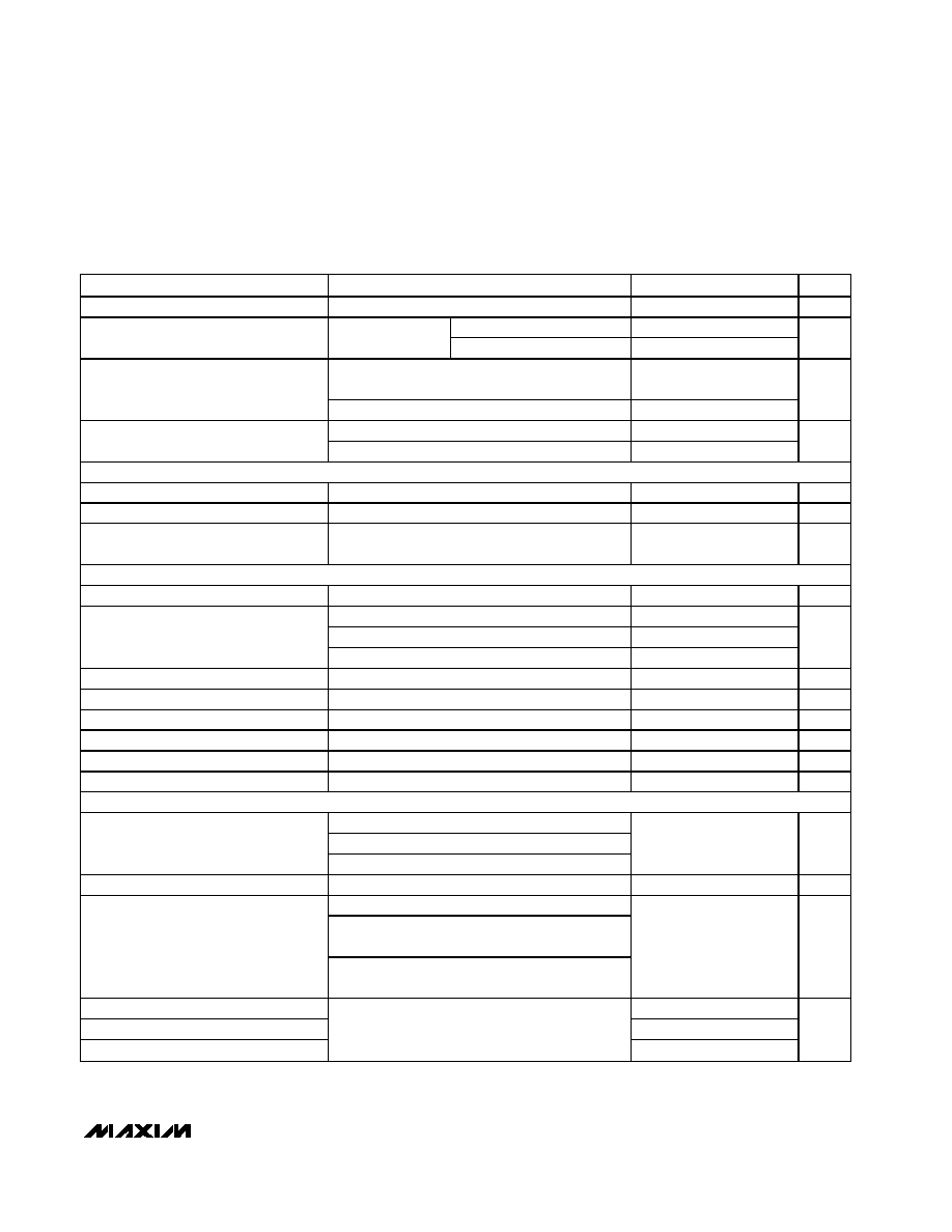
ELECTRICAL CHARACTERISTICS
(Circuit of Figure 1, V
IN
= 3V, V
DDB
= 10V, SHDN = ONDC = FREQ = IN, C
REF
= 0.22µF, PGND = GND, T
A
= 0°C to +85°C.
Typical values are at T
A
= +25
°C, unless otherwise noted.)
PARAMETER
CONDITIONS
MIN
TYP
MAX
UNITS
IN Supply Range
2.7
5.5
V
V
IN
rising
2.5
2.7
2.9
IN Undervoltage Lockout Threshold
350mV (typ)
hysteresis
V
IN
falling
2.2
2.35
2.5
V
V
FB
= V
FBP
= V
FB1
= V
FB2
= 1.5V, V
FBN
= 0
(MAX1997 only)
0.54
1.25
IN Quiescent Current (Note 1)
V
FB
= V
FBP
= 1.5V, V
FBN
= 0 (MAX1998 only)
0.476
1
mA
IN Shutdown Current
V
SHDN
= 0, V
IN
= 5.5V
0.1
1
µA
-2µA < I
REF
< 50µA
1.231
1.250
1.269
REF Output Voltage
-2µA < I
REF
< 75µA
1.225
1.250
1.275
V
Thermal Shutdown
160
°C
OVERCURRENT COMPARATOR
Input Offset Voltage
V
OCN
= V
OCP
= 1.5V to 0.8V
× V
IN
-5
+5
mV
Input Bias Current
V
OCN
= V
OCP
= 0.8V
× V
IN
-50
+50
nA
OCN, OCP Input Common-Mode Range
1.5
0.8
×
V
IN
V
FAULT TIMER
PFLT = GND (MAX1997 only)
21.8
PFLT unconnected (MAX1997 only)
43.6
Fault Timer Period
PFLT = IN, or MAX1998
87.2
ms
GATE Output Sink Current During Slew
V
GATE
= 1.5V during turn-on transition
5
10
15
µA
GATE Output Pulldown Resistance
V
GATE
< 0.5V
200
GATE Output Pullup Resistance
200
MAIN STEP-UP REGULATOR
Output Voltage Range
V
IN
13
V
FREQ = IN
1.5
FREQ unconnected
0.637
0.75
0.863
Operating Frequency
FREQ = GND
0.375
MHz
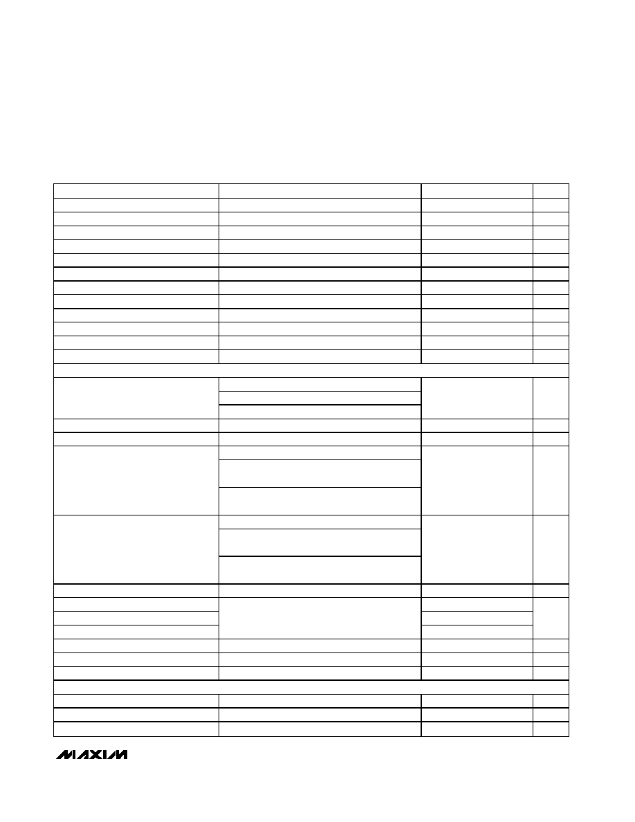
MAX1997/MAX1998
Quintuple/Triple-Output TFT LCD Power Supplies
with Fault Protection and VCOM Buffer
_______________________________________________________________________________________
3
ELECTRICAL CHARACTERISTICS (continued)
(Circuit of Figure 1, V
IN
= 3V, V
DDB
= 10V, SHDN = ONDC = FREQ = IN, C
REF
= 0.22µF, PGND = GND, T
A
= 0°C to +85°C.
Typical values are at T
A
= +25
°C, unless otherwise noted.)
PARAMETER
CONDITIONS
MIN
TYP
MAX
UNITS
Oscillator Maximum Duty Cycle
80
85
90
%
FB Regulation Voltage
I
LX
= 200mA
1.229
1.242
1.254
V
FB Fault Trip Level
V
FB
falling
0.96
1.00
1.04
V
FB Load Regulation
I
MAIN
= 0 to full load
-1.6
%
FB Line Regulation
V
IN
= 2.7V to 5.5V
0.2
0.4
%/V
FB Input Bias Current
V
FB
= 1.5V
-100
+100
nA
LX On-Resistance
250
450
m
LX Leakage Current
V
LX
= 13V
0.01
20
µA
LX Current Limit
1.6
2.1
2.8
A
LX RMS Current Rating
(Note 2)
1.4
A
Soft-Start Period
4096/f
OSC
s
Soft-Start Step Size
V
REF
/32
V
POSITIVE LINEAR-REGULATOR CONTROLLERS (REG P, REG 1, AND REG 2)
I
DRVP
= 100µA
I
DRV1
= 1350µA (MAX1997 only)
FB_ Regulation Voltage
I
DRV2
= 335µA (MAX1997 only)
1.225
1.250
1.275
V
FB_ Fault Trip Level
V
FB
_ falling
0.96
1.00
1.04
V
FB_ Input Bias Current
V
FB
_ = 1.25V
-250
+250
nA
V
DRVP
= 10V, I
DRVP
= 0.05mA to 1mA
V
DRV1
= 10V, I
DRV1
= 0.5mA to 5mA
(MAX1997 only)
FB_ Effective Load Regulation Error
(Transconductance)
V
DRV2
= 10V, I
DRV2
= 0.1mA to 2mA
(MAX1997 only)
-1.5
-2
%
I
DRVP
= 100µA, 2.7V < V
IN
< 5.5V
I
DRV1
= 1350µA, 2.7V < V
IN
< 5.5V
(MAX1997 only)
FB_ Line (IN) Regulation Error
I
DRV2
= 335µA, 2.7V < V
IN
< 5.5V
(MAX1997 only)
1
mV
Bandwidth
(Note 2)
1000
kHz
DRVP Sink Current
2
3.3
DRV1 Sink Current (MAX1997 only)
5
18
DRV2 Sink Current (MAX1997 only)
V
FB
_ = 1.1V, V
DRV
_ = 10V
5
15
mA
DRV_ Leakage Current
V
FB
_ = 1.5V, V
DRV
_ = 28V
0.1
10
µA
Soft-Start Period
4096/f
OSC
s
Soft-Start Step Size
V
REF
/32
V
NEGATIVE LINEAR-REGULATOR CONTROLLER (REG N)
FBN Regulation Voltage
I
DRVN
= 100µA
95
125
155
mV
FBN Fault Trip Level
V
FBN
rising
325
370
475
mV
FBN Input Bias Current
V
FBN
= 0V
-200
+200
nA
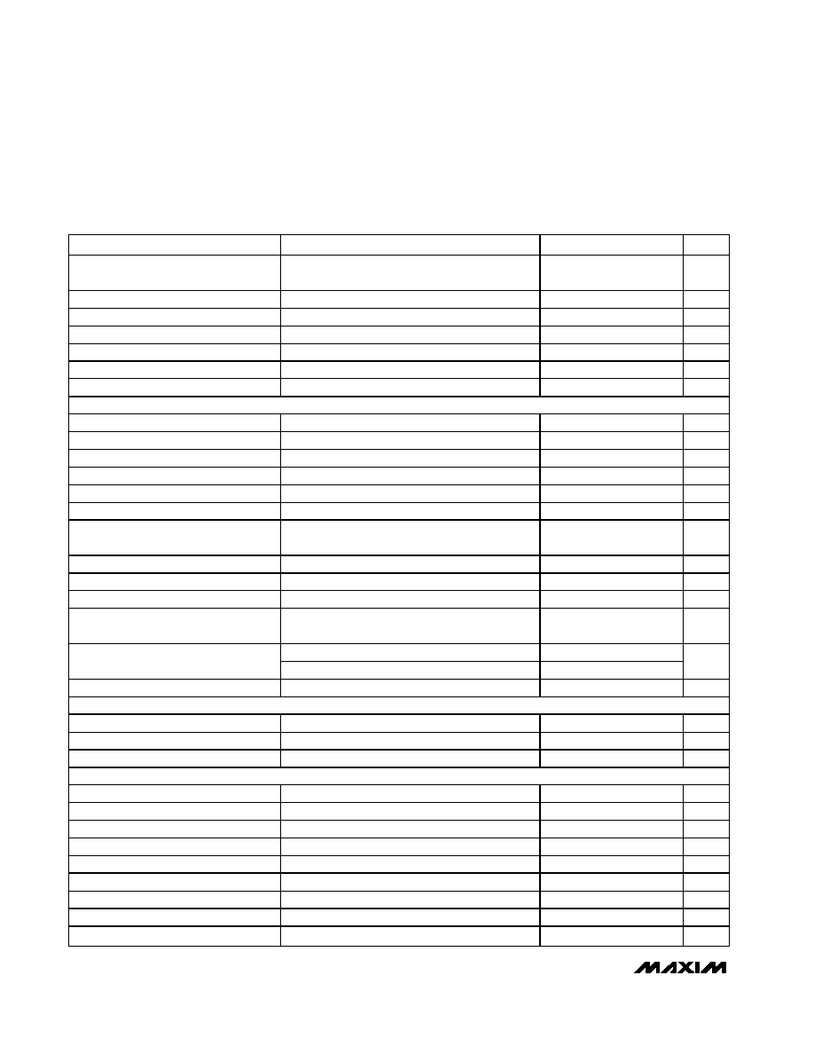
MAX1997/MAX1998
Quintuple/Triple-Output TFT LCD Power Supplies
with Fault Protection and VCOM Buffer
4
_______________________________________________________________________________________
ELECTRICAL CHARACTERISTICS (continued)
(Circuit of Figure 1, V
IN
= 3V, V
DDB
= 10V, SHDN = ONDC = FREQ = IN, C
REF
= 0.22µF, PGND = GND, T
A
= 0°C to +85°C.
Typical values are at T
A
= +25
°C, unless otherwise noted.)
PARAMETER
CONDITIONS
MIN
TYP
MAX
UNITS
FBN Effective Load Regulation Error
(Transconductance)
V
DRVN
= -10V, I
DRVN
= 50µA to 1mA
18
25
mV
FBN Line (IN) Regulation Error
I
DRVN
= 100µA, 2.7V < V
IN
< 5.5V
1
mV
Bandwidth
(Note 2)
1000
kHz
DRVN Source Current
V
FBN
= 200mV, V
DRVN
= -10V
2
4.2
mA
DRVN Leakage Current
V
FBN
= -0.1V, V
DRVN
= -20V
0.1
10
µA
Soft-Start Period
4096/f
OSC
s
Soft-Start Step Size
V
REF
/32
V
VCOM BUFFER (MAX1997 only)
V
DDB
Supply Range
4.5
13
V
V
DDB
Supply Current
V
FBPB
= V
FBNB
= 5V, V
DDB
= 9V
367
900
µA
V
DDB
Shutdown Current
V
DDB
= 13V, SHDN = ONDC = GND
3.5
13
µA
Input Offset Voltage
V
FBPB
= 2.5V, no load
-5
+5
mV
Input Bias Current
V
FBPB
= V
FBNB
= 1.2V to V
DDB
- 1.2V
1
µA
Input Offset Current
V
FBPB
= V
FBNB
= 1.2V to V
DDB
- 1.2V
-100
+100
nA
Input Common-Mode Range
V
DDB
= 4.5V to 13V
1.2
V
DDB
-
1.2
V
Power-Supply Rejection Ratio
V
DDB
= 4.5V to 13V, V
FBPB
= 2.25V
70
dB
Common-Mode Rejection Ratio
V
FBPB
= V
FBNB
= 1.2V to V
DDB
- 1.2V
70
dB
Gain-Bandwidth Product
Small signal
1/6
C
L
Hz
Load-Transient Settling Time
R
L
= 25
, C
L
= 10nF, V
DRIVE
= 9V, settle to within
10mV (Note 4)
5
µs
Small signal (
±1mV overdrive)
0.3
Transconductance
Large signal (
±30mV overdrive)
7.2
µS
Output Current Drive
±100mV overdrive, V
OUTB
= 3V or 7V
±150
±300
mA
LOGIC SIGNALS (SHDN, ONDC)
Input Low Voltage
100mV typ hysteresis
0.4
V
Input High Voltage
1.6
V
Input Current
0.01
1
µA
CONTROL INPUTS AND OUTPUTS
ONN, ONP, ON2 Comparator Offset
V
O N _
- V
CT
, V
CT
= 1.25V ±50mV
-50
+50
mV
DRVA Sink Current
V
DRVA
= 10V, V
CT
= 1.25V, V
ON2
= 2V
5
11
mA
DRVA Off-Leakage
V
DRVA
= 28V, V
CT
= 1.25V, V
ON2
= 1V
0.1
10
µA
CT Source Current
V
CT
= 1V
2.5
5
7.5
µA
CT Discharge Resistance
V
CT
= 1V
15
100
FREQ, PFLT Input Low Voltage
1
V
FREQ, PFLT Input Middle Voltage
V
IN
/2
FREQ, PFLT Input High Voltage
V
IN
- 1
V
FREQ, PFLT Input Current
FREQ, PFLT = GND or IN
-50
+50
µA
MAX1997/MAX1998
Quintuple/Triple-Output TFT LCD Power Supplies
with Fault Protection and VCOM Buffer
_______________________________________________________________________________________
5
ELECTRICAL CHARACTERISTICS
(V
IN
= 3V, V
DDB
= 10V, SHDN = ONDC = FREQ = IN, C
REF
= 0.22µF, PGND = GND, T
A
= -40°C to +85°C, unless otherwise noted.)
(Note 3)
PARAMETER
CONDITIONS
MIN
TYP
MAX
UNITS
IN Supply Range
2.7
5.5
V
V
IN
rising
2.5
2.9
IN Undervoltage Lockout Threshold
350mV typ
hysteresis
V
IN
falling
2.2
2.5
V
V
FB
= V
FBP
= V
FB1
= V
FB2
= 1.5V, V
FBN
= 0
(MAX1997 only)
1.25
IN Quiescent Current (Note 1)
V
FB
= V
FBP
= 1.5V, V
FBN
= 0 (MAX1998 only)
1
mA
-2µA < I
REF
< 50µA
1.223
1.270
REF Output Voltage
-2µA < I
REF
< 75µA
1.218
1.280
V
OVERCURRENT COMPARATOR
Input Offset Voltage
V
OCN
= V
OCP
= 1.5V to 0.8V
× V
IN
-5
+5
mV
Input Bias Current
V
OCN
= V
OCP
= 0.8V
× V
IN
-50
+50
nA
OCN, OCP Input Common-Mode Range
1.5
0.8
×
V
IN
V
MAIN STEP-UP REGULATOR
Output Voltage Range
V
IN
13
V
FREQ = IN
1
2
FREQ unconnected
0.563
0.937
Operating Frequency
FREQ = GND
0.25
0.50
MHz
Oscillator Maximum Duty Cycle
78
92
%
FB Regulation Voltage
I
LX
= 200mA
1.215
1.260
V
FB Fault Trip Level
V
FB
falling
0.96
1.04
V
FB Input Bias Current
V
FB
= 1.5V
-100
+100
nA
LX On-Resistance
450
m
LX Current Limit
1.6
2.8
A
POSITIVE LINEAR-REGULATOR CONTROLLERS (REG P, REG 1, AND REG 2)
I
DRVP
= 100µA
I
DRV1
= 1350µA (MAX1997 only)
FB_ Regulation Voltage
I
DRV2
= 335µA (MAX1997 only)
1.213
1.288
V
FB_ Fault Trip Level
V
FB
_ falling
0.96
1.04
V
V
DRVP
= 10V, I
DRVP
= 0.05mA to 1mA
V
DRV1
= 10V, I
DRV1
= 0.5mA to 5mA
(MAX1997 only)
FB_ Effective Load Regulation Error
(Transconductance)
V
DRV2
= 10V, I
DRV2
= 0.1mA to 2mA
(MAX1997 only)
-2.5
%
DRVP Sink Current
1
DRV1 Sink Current (MAX1997 Only)
5
DRV2 Sink Current (MAX1997 Only)
V
FB
_ = 1.1V, V
DRV
_ = 10V
5
mA