_______________General Description
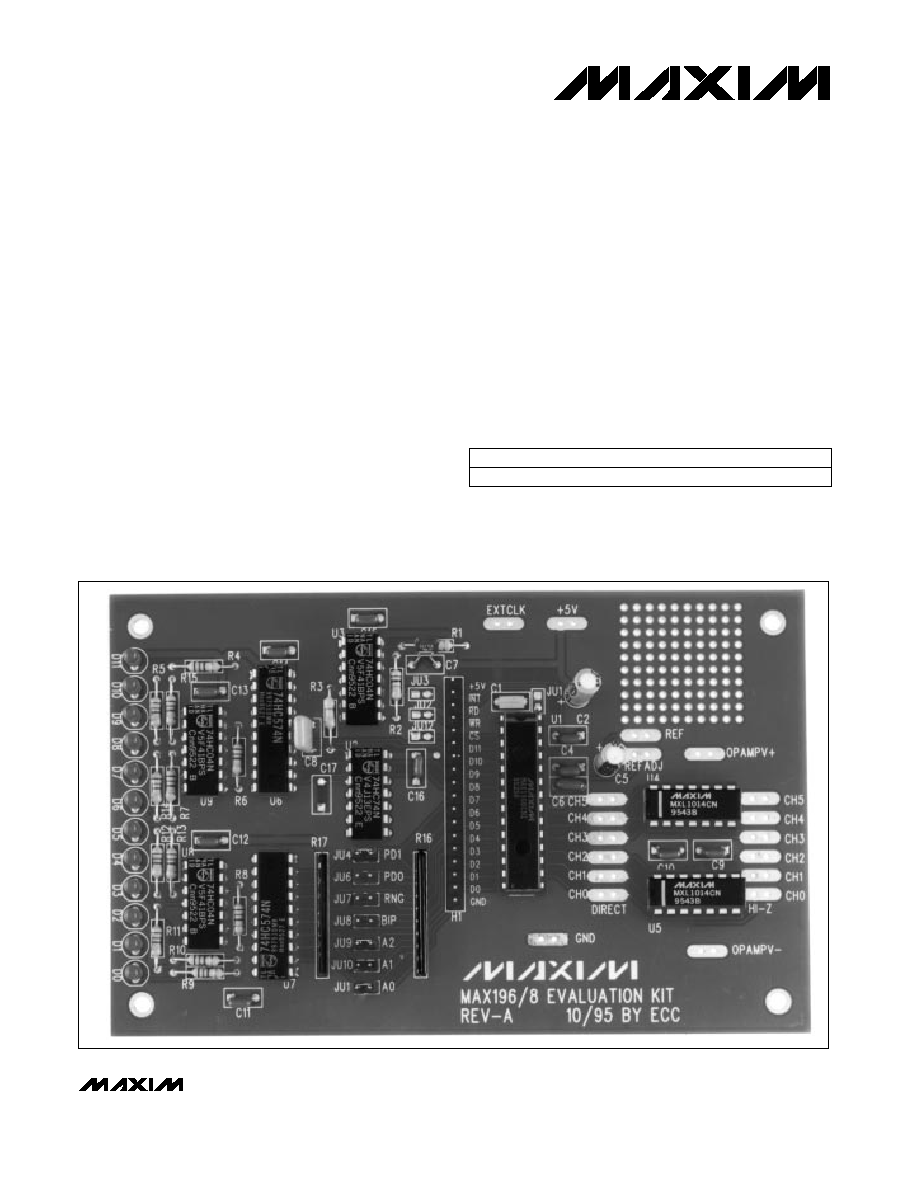
The MAX196 evaluation kit (EV kit) is an assembled and
tested board for prototyping designs using the MAX196
12-bit, multi-range data-acquisition system (DAS). The
board includes voltage buffers for all six analog input
channels, and is designed to be operated in a stand-
alone demo mode using a binary LED readout. It can
be adapted to a user-provided 16-bit microprocessor
(µP) bus. The EV kit requires a +5V power supply for
the MAX196 and ±15V power supplies for the op amps.
The MAX196 EV kit evaluates both the MAX196 and the
MAX198. To evaluate the MAX198, order a free sample
of the MAX198BCNI along with the MAX196 EV kit.
Maxim also offers a complete µP-based EV system for
the 8-bit interface version of this device, the MAX197.
Refer to the MAX197 EV kit manual.
____________________________Features
o
Stand-Alone Demo
o
Proven PC Board Layout
o
User Prototype Area
o
Fully Assembled and Tested
o
Jumper-Selectable Configuration
Evaluates: MAX196/MAX198
MAX196 Evaluation Kit
________________________________________________________________
Maxim Integrated Products
1
19-0473; Rev 0; 2/96
PART
TEMP. RANGE
BOARD TYPE
MAX196EVKIT-DIP
+25°C
Through-Hole
______________Ordering Information
________________________________________________________________________EV Kit
For free samples & the latest literature: http://www.maxim-ic.com, or phone 1-800-998-8800
_________________________Quick Start
The MAX196 EV kit is fully assembled and tested.
Follow these steps to verify board operation.
Do not
turn on the power supply until all connections are
completed.
1) Connect a +5V supply to the pad labeled +5V, and
connect the ground return to the pad labeled GND.
2) Connect ±15V supplies to the pads labeled, respec-
tively, OPAMPV+ and OPAMPV-. Connect the power
supply's common terminal to the EV kit's GND pad.
3) Set configuration jumpers as shown in Table 1. This
selects channel 0 with a ±10V input range and puts
the device in no power-down/internal clock mode.
4) Apply an input signal to the "high-Z" channel 0 input
pad located at the far-right side of the board.
5) Turn on the power supplies.
6) Observe binary readout on the twelve LEDs.
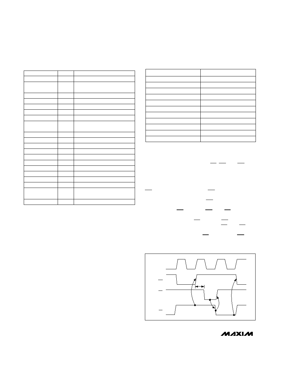
_______________Detailed Description
Stand-Alone Demo Circuit Operation
The demo circuit is a state-machine driven by a 1kHz
system clock that generates the RD, WR, and INT puls-
es. The circuit runs continuously, writing the command
word programmed by the jumpers, and displaying the
results on the LEDs.
At power-up, R3 and C8 reset flip-flop, U2, generating a
WR pulse. On the rising edge of WR, the MAX196 latches
the command word selected by JU4JU11. The rising
edge of the system clock sets WR high, initiating a con-
version. When the MAX196 completes the conversion, the
MAX196 drives INT low. After INT falls, RD goes low at
the next rising edge of the system clock, placing the data
onto the data bus. When RD goes low, INT goes high, so
that the next system clock cycle drives RD high. RD's ris-
ing edge latches the data into U6 and U7. U8 and U9
drive the LED display. After RD returns high, WR goes
low, and the cycle repeats (Figure 1).
Evaluates: MAX196/MAX198
MAX196 Evaluation Kit
2
_______________________________________________________________________________________
Table 1. Default Jumper Settings
JUMPER
SETTING
JU1
Short (default trace)
JU2
Short (default trace)
JU3
Short (default trace)
JU4 (PD1)
Short
JU7 (RNG)
Open
JU5 (PD0)
Open
JU8 (BIP)
Open
JU10 (A1)
Short
JU9 (A2)
Short
JU11 (A0)
Short
JU12
Short (default trace)
____________________Component List
DESIGNATION
QTY
DESCRIPTION
C1
1
100pF ceramic capacitor
C2, C4,
C9C16
10
0.1µF ceramic capacitors
C3, C5
2
10µF ceramic capacitors
C6
1
0.01µF ceramic capacitor
C7
1
0.22µF ceramic capacitor
H1
1
18-pin header
JU1, JU2,
JU3, JU12
0
Open
JU4, JU6JU11
7
2-pin jumpers
D0D11
12
LEDs
SYSTEM
CLOCK
WR
t
CONV
INT
RD
Figure 1. MAX196 Stand-Alone Demo Circuit Timing Diagram
R1, R2
2
10k
, 5% resistors
R4R15
12
620
, 5% resistors
R16
1
10k
, 9-pin SIP resistor
R17
1
100k
, 9-pin SIP resistor
U1
1
Maxim MAX196BCNI
U2
1
74HC74 dual flip-flop
U3, U8, U9
3
74HC04 hex inverter
U4, U5
2
Maxim MXL1014CN quad
op amps
U6, U7
2
74HC574 octal latch
C8
1
1µF ceramic capacitor
R3
1
470k
, 5% resistor

Optional Input Buffers
The op amp buffers are MXL1014 precision quad op
amps, connected in voltage-follower configurations.
These op amps should normally be powered from ±15V
(±22V absolute maximum). Applications that use only
0V to 4V signals may power the MXL1014 from ±5V
with good results.
The MAX196 should be driven from a low output
impedance signal source (such as an op amp). To use
the on-board op amps, drive the HI-Z CH0CH5 input
pads. When using an off-board low-impedance source,
unplug the MXL1014s and drive the DIRECT CH0CH5
input pads.
Configuring the MAX196
Tables 2, 3, and 4 show the jumper connections for the
different operating modes of the MAX196 EV kit. Refer
to Table 2 for clock and power-down modes, Table 3
for input range selection, and Table 4 for channel
selection.
Using an External Clock
As shipped from the factory, the MAX196 EV kit uses
C1 as a timing capacitor for internal clock mode. To
use an external clock, cut JU1 and apply the external
clock source to the EXTCLK input pad. Start up the kit
with JU4 (PD1) and JU5 (PD0) shorted.
Evaluating the MAX198
To evaluate the MAX198, remove the MAX196 and
replace it with a MAX198BCNI.
Interfacing to a 16-Bit Bus
The MAX196/MAX198 are designed to connect directly
to a 16-bit µP bus using standard chip-select (CS),
read strobe (RD), and write strobe (WR) signals. JU2,
JU3, and JU12 must be cut to disable the stand-alone
circuit (Table 5). All interface signals are provided on
header H1. For interface details, refer to the
MAX196/MAX198 data sheet.
Evaluates: MAX196/MAX198
MAX196 Evaluation Kit
_______________________________________________________________________________________
3
Table 3. Range and Polarity Selection
Table 4. Channel Selection
Table 5. Demo Circuit Jumpers
Table 2. Clock and Power-Down
Selection
JU4
(PD1)
FUNCTION
Open
Short
No power-down, external
clock mode
Standby power-down
between readings
Short
No power-down, internal
clock mode
Open
Full power-down between
readings
JU5
(PD0)
Short
Short
Open
Open
JU1
X
Open
Short
X
JU8
(BIP)
MAX196
INPUT RANGE (V)
Open
Short
0 to 5
±5
Short
0 to 10
Open
±10
JU7
(RNG)
Short
Short
Open
Open
MAX198
INPUT RANGE (V)
0 to V
REF
/2
±V
REF
/2
0 to V
REF
±V
REF
JU9
(A2)
JU11
(A0)
Short
Short
Short
Short
Short
Open
Short
Open
JU10
(A1)
Open
Short
Short
Open
CHANNEL
CH0
CH2
CH1
CH3
Open
Short
Open
Open
Short
Short
CH4
CH5
JU2
JU12
Short
Short
Open
Open
JU3
Short
Open
MODE
Stand-alone demo
Connect to a user-
provided system

Evaluates: MAX196/MAX198
MAX196 Evaluation Kit
4
_______________________________________________________________________________________
R4R15, 620
D11
12
10
13
19
18
17
16
15
14
13
12
19
18
17
16
15
14
13
12
2
3
4
5
6
7
8
9
+5V
+5V
+5V
+5V
+5V
+5V
+5V
+5V
JU4
JU12
CUTHERE
JU1
CUTHERE
C1
100pF
C2
0.1
µ
F
C3
10
µ
F
C5
10
µ
F
C4
0.1
µ
F
C6
0.01
µ
F
C9
0.1
µ
F
C10
0.1
µ
F
U1
R17, 100k
R16
10k
D7
2
3
4
5
6
7
8
9
D6
D5
D4
D3
D2
D1
D0
JU6
JU7
JU8
JU9
JU10
JU11
D11
D10
D9
D8
2
11
1
3
4
5
6
7 8
9
D0
D1
D2
D3
D4
D5
D6
D7
11
5
11
5
1
1
9
9
3
3
6
10
13
6
2
2
8
12
U9E
74HC04
U9F 74HC04
U9D 74HC04
U8F 74HC04
U8D 74HC04
U8B 74HC04
U9B 74HC04
U9C
74HC04
74HC574
74HC574
U8E
74HC04
U8C
74HC04
U8A
74HC04
U9A
74HC04
8
4
4
D10
D8
D1
D3
D5
D7
D9
D0
D2
D4
D6
D0
D1
D2
D3
D4
D5
D6
D7
Q0
U7
U6
RD DEMO
H114
H113
H118
H115
H117
REF
H11
GND
BYPASS CAPACITORS
REFADJ
OPAMPV+
OPAMPV-
H116
H112
H111
H110
H19
H18
H17
H16
H15
H14
H13
H12
EXTCLK
1
2
3
28
+5V
27
26
13
12
25
24
23
22
21
20
19
18
17
14
CH5 HI-Z
CH4 HI-Z
CH3 HI-Z
CH2 HI-Z
CH1 HI-Z
CH0 HI-Z
HI-Z
INPUTS
DIRECT
INPUTS
CH5
CH4
CH3
CH2
CH1
CH0
7
1
14
7
1
16
15
D11
D10
D9
D8
D7
D5
D4
D3
D2
D1
D0
D6
4
5
7
8
9
10
11
12
13
14
6
RD DEMO
WR DEMO
CLK
Q1
Q2
Q3
Q4
Q5
Q6
Q7
D0
D1
D2
D3
D4
D5
D6
D7
Q0
Q1
Q2
Q3
Q4
Q5
Q6
Q7
<
OE
11
1
CLK
<
OE
D11
WR
WR
CS
V
DD
CLK
DGND
D10
RD
D9
INT
D8
REF
D7
REF ADJ
D6
CH5
D5
CH4
D4
CH3
D3
CH2
D2
CH1
D1
CH0
D0
GND
RDDEMO
74HC74
74HC74
74HC04
74HC04
74HC04
RD DEMO
10
11
1
2
3
4
6
5
8
9
13
12
U3F
U3E
U3D
11
10
9
8
12
R1
10k
R3
470k
R2
+5V
10k
13
+5V
+5V
+5V
+5V
R
S
INT
Q
Q
D
>CLK
RD
WR
JU3
CUTHERE
JU2
CUTHERE
C16
0.1
µ
F
C15
0.1
µ
F
C14
0.1
µ
F
C11
0.1
µ
F
C12
0.1
µ
F
C13
0.1
µ
F
C8
1
µ
F
C17
OPEN
C7
0.22
µ
F
WR DEMO
U2B
R
S
Q
Q
D
>CLK
U2A
RD
INT
+
+
+
-
6
5
+
-
2
3
+
-
13
12
+
-
6
5
+
-
2
3
+
-
BYPASS
CAPACITORS
+5V
MAX196
MXL1014
U4D, U4B, U4A
MXL1014
U5D, U5B, U5A
Figure 2. MAX196 EV Kit Schematic
Evaluates: MAX196/MAX198
MAX196 Evaluation Kit
_______________________________________________________________________________________
5
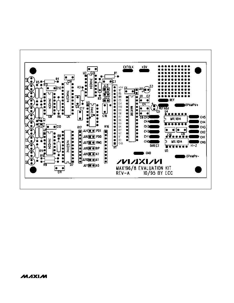
Figure 3. MAX196 EV Kit Component Placement Guide--Component Side