MAX1958EV Kit
General Description
The MAX1958/MAX1959 evaluation (EV) kit demonstrates
an application circuit ideal for use with hetero-junction
bipolar transistor power amplifiers (HBT PA). The
MAX1958/MAX1959 application circuit features an
800mA DC-to-DC buck converter, an operational amplifier,
and a high-accuracy temperature sensor.
The high-efficiency, dynamically adjustable, pulse-width
modulated (PWM), DC-to-DC buck converter is opti-
mized to provide power to the HBT PA in N-CDMA and
W-CDMA cellular phones. The 1MHz PWM switching fre-
quency allows the use of small external components,
while skip mode reduces quiescent current to 190µA
with light loads. The buck regulator is dynamically con-
trolled to provide any fixed output voltage in the 0.75V to
3.4V (MAX1958) and 1V to 3.6V (MAX1959) ranges. The
DC-to-DC converter utilizes a low on-resistance internal
MOSFET switch and synchronous rectifier to maximize
efficiency and minimize external component count.
The built-in operational amplifier is used to provide full
bias control for the PA to maximize efficiency. The
amplifier has Rail-to-Rail
®
input/output capability,
800kHz gain-bandwidth product, and 120dB open-loop
voltage gain. An added feature of the amplifier is an
active output discharge in shutdown mode.
The precision temperature sensor measures tempera-
tures between -40°C and +125°C.
This fully tested EV kit comes with the MAX1958 IC
installed. The MAX1959 has an identical pinout
arrangement and can be evaluated on this board. To
evaluate the MAX1959, request a free sample of the
MAX1959 when ordering this evaluation kit.
Features
o Buck Converter
Dynamically Adjustable Output from 0.75V to
3.4V (MAX1958)
Dynamically Adjustable Output from 1V to
3.6V (MAX1959)
1MHz Fixed-Frequency PWM
800mA Guaranteed Output Current
130mV IC Dropout at 600mA Load
16% to 100% Duty-Cycle Operation
Low Quiescent Current
190µA (typ) in Skip Mode (MAX1958)
3mA (typ) in PWM Mode
0.01µA (typ) in Shutdown Mode
No External Schottky Diode Required
o Operational Amplifier
Active Output Discharge in Shutdown Mode
800kHz Gain-Bandwidth Product
120dB Open-Loop Voltage Gain (R
L
= 100k
)
5mA Rail-to-Rail Output
o Temperature Sensor
-40°C to +125°C Rated Temperature Range
Accurate Sensor, -11.64mV/°C Slope
Evaluates: MAX1958/MAX1959
MAX1958/MAX1959 Evaluation Kit
________________________________________________________________ Maxim Integrated Products
1
19-2775; Rev 0; 2/03
For pricing, delivery, and ordering information, please contact Maxim/Dallas Direct! at
1-888-629-4642, or visit Maxim's website at www.maxim-ic.com.
Ordering Information
PART
TEMP RANGE
IC PACKAGE
MAX1958EVKIT
-40°C to +85°C
20 Thin QFN
Rail-to-Rail is a registered trademark of Nippon Motorola, Ltd.
Note: When contacting these component suppliers, please specify you are using the MAX1958/MAX1959.
Component Suppliers
SUPPLIER
COMPONENT
PHONE
WEBSITE
Kamaya
Resistors
260-489-1533
www.kamaya.com
Murata
Capacitors
770-436-1300
www.murata.com
Sumida
Inductors
81-03-3667-3381
www.sumida.com
Taiyo Yuden
Capacitors
408-573-4150
www.t-yuden.com
Evaluates: MAX1958/MAX1959
Required Equipment
The following equipment is required before beginning:
· Three 6V (at 1A) DC power supplies or batteries
· Digital multimeter (DMM)
· Temperature gauge
· Current meter (optional)
Quick Start
The MAX1958 application circuit is fully assembled and
tested. Follow these steps to verify board operation.
DC-to-DC Converter
1) Preset one DC power supply (PS1) to 2.6V. Turn off
the power supply.
2) Preset the second DC power supply (PS2) to 0.43V.
Turn off the power supply.
3) Verify that the shunt is in place at JU1 between
positions 2 and 3 for normal-mode operation.
4) Verify that there is no shunt at JU2.
5) Connect the positive lead of PS1 to the VIN pad and
connect the negative lead of PS1 to GND.
6) Connect the positive lead of PS2 to the ADJ pad
and connect the negative lead of PS2 to GND5.
7) Connect the positive lead of the DMM to VOUT and
connect the negative lead of the DMM to GND3.
This DMM measures the output voltage at VOUT.
8) Turn on both of the power supplies (PS1 first, then PS2).
9) Verify that the voltage at VOUT is 0.75V.
10) Gradually increase the PS1 output voltage up to
4.7V verifying that the output voltage at VOUT
remains at 0.75V. VOUT does not regulate to 0.75V
at input voltages above 4.7V due to the minimum
duty-cycle range.
11) Gradually increase the output of the PS2 power
supply up to 1.93V verifying that the output voltage
tracks the ADJ voltage at (1.76
V
ADJ
). When V
ADJ
is 1.93V, V
OUT
should be 3.4V.
12) With V
ADJ
set at 0.57V, gradually increase the output
voltage of PS1 to 5.5V verifying that the VOUT output
voltage remains at 1V.
13) Connect an 800mA load between VOUT and GND3.
14) Verify that the voltage at VOUT is 1V.
Operational Amplifier
MAX1958/MAX1959 Evaluation Kit
2
_______________________________________________________________________________________
Component List
DESIGNATION
QTY
DESCRIPTION
C1, C3
2
4.7µF
±10%, 6.3V ceramic
capacitors
Taiyo Yuden JMK212BJ475KG
C2, C7
2
0.1µF
±10%, 50V X7R ceramic
capacitors
Taiyo Yuden EMK107BJ104KA
C4, C8, C9, C10
4
Not installed
C5
1
0.01µF ±10%, 50V X7R ceramic
capacitor
Taiyo Yuden UMK107 B103KZ
C6
1
560pF
±5%, 50V SL ceramic
capacitor
Murata GRM1881X1H561J
C11
1
22pF ±5%, 50V SL ceramic
capacitor
Murata GRM1881X1H220J
C12
1
100pF ±5%, 50V SL ceramic
capacitor
Murata GRM1881X1H101J
JU1
1
Jumper, SIP3, 3-pin header
Digikey S1012-3-ND
JU2, JU3, JU4
3
Jumpers, SIP2, 2-pin headers
Digikey S1012-2-ND
L1
1
4.7µH, 900mA power inductor
Sumida CDRH3D16-4R7
R1
1
20
±5% resistor
R2
1
6.8k
±5% resistor
R3
1
12k
±5% resistor
R4
1
9.1k
±5% resistor
R5, R9, R10
3
Not installed
R6, R7, R8
3
1M
±5% resistors
R11
1
100
±5% resistor
None
2
BNC connectors
A/D Electronics 580-002-00
U1
1
MAX1958ETP

1) Preset one DC power supply (PS1) to 2.6V. Turn off
the power supply.
2) Preset another DC power supply (PS3) to 1V. Turn
off the power supply.
3) Verify that there is no shunt across JU4.
4) Connect the positive lead of PS1 to the VIN pad and
connect the negative lead of PS1 to the GND pad.
5) Connect the positive lead of PS3 to the IN+ pad and
connect the negative lead of PS3 to the GND4 pad.
6) Connect the positive lead of the DMM to AOUT.
Connect the negative lead of the DMM to GND1.
The DMM now measures the output voltage, AOUT.
7) Turn on the power supplies (PS1 first and then PS3).
8) Verify the output voltage at AOUT is 1.57V.
9) Gradually increase the output voltage of PS3 and
verify that the voltage at AOUT is (1.57
V
IN+
).
V
AOUT
cannot be higher than (V
IN
- 25mV).
10) Gradually increase the output voltage of PS1 up to
5.5V verifying that the output voltage remains at
(1.57
V
IN+
).
Temperature Sensor
1) Preset a DC power supply (PS1) to 2.6V. Turn off
the power supply.
2) Verify that there is no shunt across JU3.
3) Connect the positive lead of PS1 to the VIN pad and
connect the negative lead of PS1 to the GND pad.
4) Place the input of the temperature gauge as close
to the IC as possible. For best results, solder a ther-
mocouple to the via connected to the exposed pad
on the back of the IC.
5) Turn on the power supply.
6) Measure the voltage at TOUT. Compare this voltage
with the output of the temperature gauge. See the
Temperature Sensor Operation section for the TOUT
voltage calculation.
Detailed Description
Setting the Output Voltage
The MAX1958's output voltage tracks the voltage at
ADJ. V
OUT
should regulate at 1.76
V
ADJ
for the
MAX1958 and 2
V
ADJ
- 0.8 for the MAX1959.
Temperature Sensor Operation
The temperature sensor provides information about the
MAX1958/MAX1959 die temperature. The voltage at
TOUT (V
TOUT
) is found as follows:
This equation can be approximated with the linear
function:
The temperature sensor provides accurate information
about the die temperature. Additional error in the temper-
ature output caused by die self-heating may exist. Refer
to the Temperature Sensor section in the MAX1958/
MAX1959 data sheet for more details.
Operational Amplifier Operation
The MAX1958 EV kit demonstrates the operational
amplifier in the MAX1958 in a noninverting configuration
with a gain of 1.57V/V. Resistors R2 and R3 can be
changed to alter the noninverting gain. The following
equation shows the relationship between R2 and R3 to
determine gain.
Jumper Settings
Jumper JU2/JU3/JU4 Functions
(Shutdown)
The MAX1958/MAX1959 feature a shutdown mode to
minimize the quiescent current. Place a shunt between
pins 1 and 2 on JU2 to shutdown the DC-to-DC converter.
Place a shunt between pins 1 and 2 on JU4 to shutdown
the operational amplifier. Place a shunt between pins 1
and 2 on JU3 to shutdown the temperature sensor.
Remove the shunts for normal operation.
Jumper JU1 Function (Mode Select)
The DC-to-DC converter contained in the MAX1958/
MAX1959 can be operated in two modes. Place a shunt
between pins 1 and 2 on JU1 to operate in forced-PWM
mode at all loads. Place a shunt between pins 2 and 3
on JU1 to operate in skip mode at light loads (<150mA)
and PWM mode at medium to heavy loads. Do not
leave JU1 unconnected.
V
V
R
R
AOUT
IN
=
×
+
+
2
3
1
V
mV
C
T
TOUT
.
.
=
°
×
+
-11 64
1 8778
V
TOUT
=
×
×
+
×
×
+
-4 10
T
-1.13 10
T
-6
2
-2
1 8708
.
Evaluates: MAX1958/MAX1959
MAX1958/MAX1959 Evaluation Kit
_______________________________________________________________________________________
3
Evaluates: MAX1958/MAX1959
MAX1958/MAX1959 Evaluation Kit
4
_______________________________________________________________________________________
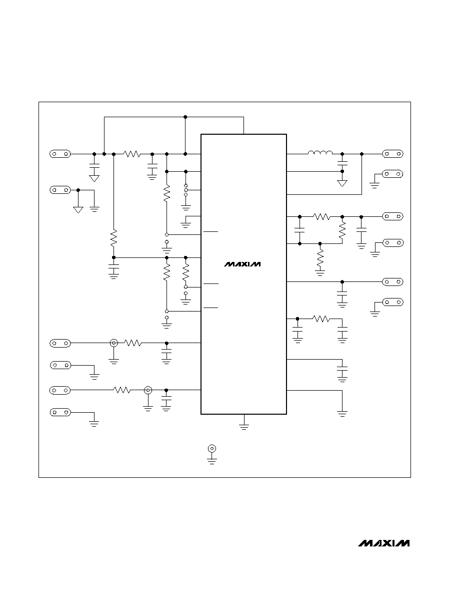
MAX1958
U1
IN
R9
OPEN
C1
4.7
µF
C9
OPEN
R1
20
R7
1M
R8
1M
R6
1M
C2
0.1
µF
C10
OPEN
C8
OPEN
VIN
2.6V TO 5.5V
GND
IN
PWM
AGND
SHDN1
V
CC
SHDN2
SHDN3
ADJ
EXPOSED PAD
IN+
LX
14
C3
4.7
µF
VOUT
GND3
AOUT
GND1
TOUT
GND2
R4
9.1k
R11
100
C12
100pF
R2
6.8k
R3
12k
C4
OPEN
C5
0.01
µF
C6
560pF
C7
0.1
µF
C11
22pF
12
10
11
1
20
4
7
5
3
13
16
JU1
JU4
JU3
JU2
R10
SHORT
R5
SHORT
ADJ
GND5
IN+
GND4
15
6
17
18
2
9
8
19
BNC CONNECTOR
PGND
OUT
AOUT
IN-
TOUT
COMP
REF
AGND
INP
L1
4.7
µH
SUMIDA CDRH3D16-4R7
1
2
3
2
1
2
1
2
1
Figure 1. MAX1958/MAX1959 EV Kit Schematic
Evaluates: MAX1958/MAX1959
MAX1958/MAX1959 Evaluation Kit
_______________________________________________________________________________________
5
1.994in
2.713in
1.994in
2.713in
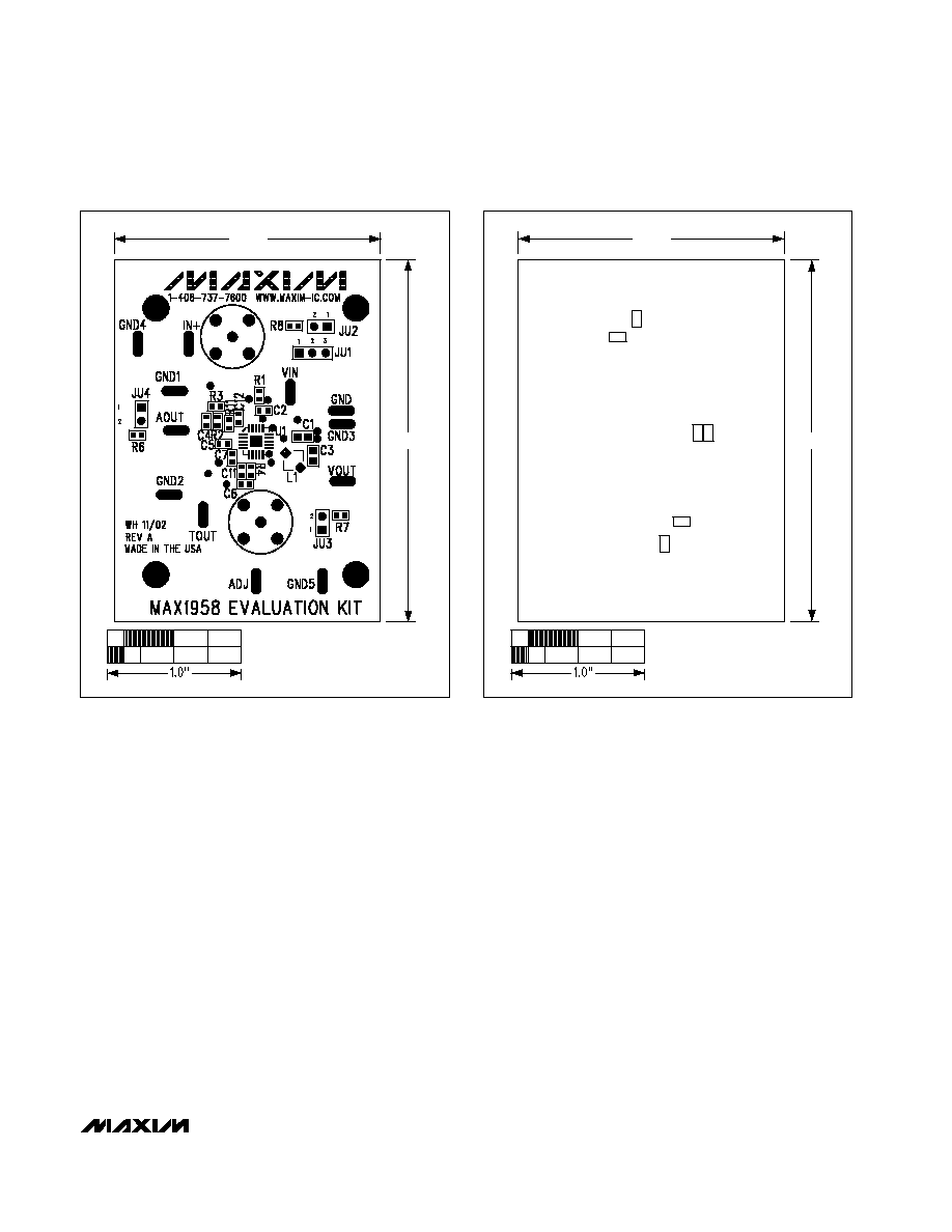
Figure 2. MAX1958 EV Kit Component Placement Guide--Top
Silkscreen
Figure 3. MAX1958 EV Kit Component Placement Guide--
Back Silkscreen