General Description
The MAX19586 is a 3.3V, high-speed, high-perfor-
mance analog-to-digital converter (ADC) featuring a
fully differential wideband track-and-hold (T/H) and a
16-bit converter core. The MAX19586 is optimized for
multichannel, multimode receivers, which require the
ADC to meet very stringent dynamic performance
requirements. With a -82dBFS noise floor, the
MAX19586 allows for the design of receivers with supe-
rior sensitivity requirements.
At 80Msps, the MAX19586 achieves a 79.2dB signal-to-
noise ratio (SNR) and an 84.3dBc/100dBc single-tone
spurious-free dynamic range (SFDR) performance
(SFDR1/SFDR2) at f
IN
= 70MHz. The MAX19586 is not
only optimized for excellent dynamic performance in
the 2nd Nyquist region, but also for high-IF input fre-
quencies. For instance, at 130MHz, the MAX19586
achieves an 82.5dBc SFDR and its SNR performance
stays flat (within 2.5dB) throughout the 4th Nyquist
region. This level of performance makes the part ideal
for high-performance digital receivers.
The MAX19586 operates from a 3.3V analog supply
voltage and a 1.8V digital voltage, features a 2.56V
P-P
full-scale input range, and allows for a guaranteed sam-
pling speed of up to 80Msps. The input track-and-hold
stage operates with a 600MHz full-scale, full-power
bandwidth.
The MAX19586 features parallel, low-voltage CMOS-
compatible outputs in two's-complement output format.
The MAX19586 is manufactured in an 8mm x 8mm,
56-pin thin QFN package with exposed paddle (EP) for
low thermal resistance, and is specified for the extend-
ed industrial (-40°C to +85°C) temperature range.
Applications
Cellular Base-Station Transceiver Systems (BTS)
Wireless Local Loop (WLL)
Multicarrier Receivers
Multistandard Receivers
E911 Location Receivers
High-Performance Instrumentation
Antenna Array Processing
Features
o 80Msps Minimum Sampling Rate
o -82dBFS Noise Floor
o Excellent Dynamic Performance
80dB/79.2dB SNR at f
IN
= 10MHz/70MHz
and -2dBFS
96dBc/102dBc Single-Tone SFDR1/
SFDR2 at f
IN
= 10MHz
84.3dBc/100dBc Single-Tone SFDR1/
SFDR2 at f
IN
= 70MHz
o Less than 0.1ps Sampling Jitter
o 1.1W Power Dissipation
o 2.56V
P-P
Fully Differential Analog Input Voltage
Range
o CMOS-Compatible Two's-Complement Data
Output
o Separate Data Valid Clock and Over-Range
Outputs
o Flexible Input Clock Buffer
o 3.3V Analog Power Supply; 1.8V Digital Output
Supply
o Small 8mm x 8mm x 0.8mm 56-Pin Thin QFN
Package
o EV Kit Available for MAX19586
(Order MAX19586EVKIT)
MAX19586
High-Dynamic-Range, 16-Bit,
80Msps ADC with -82dBFS Noise Floor
________________________________________________________________ Maxim Integrated Products
1
TOP VIEW
MAX19586
THIN QFN
8mm x 8mm
15
17
16
18
19
20
21
22
23
24
25
26
27
28
N.C.
N.C.
AV
DD
AV
DD
AV
DD
AGND
AGND
AGND
AV
DD
AV
DD
AV
DD
REFOUT
REFIN
AGND
AV
DD
AV
DD
N.C.
DOR
DGND
DV
DD
DAV
D15
D14
D13
D12
D11
D10
D9
48
47
46
45
44
43
54
53
56
55
52
51
50
49
1
2
3
4
5
6
7
8
9
10
11 12 13 14
42 41 40 39 38 37 36 35 34 33 32 31 30 29
AGND
AGND
AGND
INN
INP
AGND
AGND
AGND
AGND
CLKN
CLKP
AGND
AV
DD
AV
DD
DGND
DGND
DV
DD
D0
D1
D2
D3
D4
D5
D6
D7
D8
DV
DD
DV
DD
Pin Configuration
Ordering Information
19-3758; Rev 0; 8/05
For pricing, delivery, and ordering information, please contact Maxim/Dallas Direct! at
1-888-629-4642, or visit Maxim's website at www.maxim-ic.com.
EVALUATION KIT
AVAILABLE
+Denotes lead-free package.
PART
TEMP RANGE
PIN-PACKAGE
PKG
CODE
MAX19586ETN
-40
°C to +85°C 56 Thin QFN-EP T5688-2
MAX19586ETN+
-40
°C to +85°C 56 Thin QFN-EP T5688-2

MAX19586
High-Dynamic-Range, 16-Bit,
80Msps ADC with -82dBFS Noise Floor
2
_______________________________________________________________________________________
ABSOLUTE MAXIMUM RATINGS
ELECTRICAL CHARACTERISTICS
(AV
DD
= 3.3V, DV
DD
= 1.8V, AGND = DGND = 0, INP and INN driven differentially, internal reference CLKP and CLKN driven differentially,
C
L
= 5pF at digital outputs, f
CLK
= 80MHz, T
A
= T
MIN
to T
MAX
, unless otherwise noted. Typical values are at T
A
= +25°C, unless otherwise
noted.) (Note 1)
Stresses beyond those listed under "Absolute Maximum Ratings" may cause permanent damage to the device. These are stress ratings only, and functional
operation of the device at these or any other conditions beyond those indicated in the operational sections of the specifications is not implied. Exposure to
absolute maximum rating conditions for extended periods may affect device reliability.
AV
DD
to AGND ..................................................... -0.3V to +3.6V
DV
DD
to DGND..................................................... -0.3V to +2.4V
AGND to DGND.................................................... -0.3V to +0.3V
INP, INN, CLKP, CLKN, REFP, REFN,
REFIN, REFOUT to AGND....................-0.3V to (AV
DD
+ 0.3V)
D0D15, DAV, DOR, DAV to GND...........-0.3V to (DV
DD
+ 0.3V)
Continuous Power Dissipation (T
A
= +70°C)
56-Pin Thin QFN
(derate 47.6mW/°C above +70°C) .........................3809.5mW
Operating Temperature Range ..........................-40°C to +85°C
Thermal Resistance
JA
..................................................21°C/W
Thermal Resistance
JC
.................................................0.6°C/W
Junction Temperature ......................................................+150°C
Storage Temperature Range .............................-60°C to +150°C
Lead Temperature (soldering, 10s) .................................+300°C
PARAMETER
SYMBOL
CONDITIONS
MIN
TYP
MAX
UNITS
DC ACCURACY
Resolution
N
16
Bits
Offset Error
VOS
0
10
20
mV
Gain Error
GE
-3.5
+3.5
%FS
ANALOG INPUTS (INP, INN)
Input Voltage Range
V
DIFF
Fully differential input, V
IN
= V
INP
- V
INN
2.56
V
P-P
Common-Mode Voltage
V
CM
Internally self-biased
2.2
V
Differential Input Resistance
R
IN
10
±20%
k
Differential Input Capacitance
C
IN
7
pF
Full-Power Analog Bandwidth
BW
-3dB
-3dB rolloff for FS Input
600
MHz
REFERENCE INPUT/OUTPUT (REFIN, REFOUT)
Reference Input Voltage Range
REFIN
1.28
±10%
V
Reference Output Voltage
REFOUT
1.28
V
DYNAMIC SPECIFICATIONS (f
CLK
= 80Msps)
Thermal Plus Quantization Noise
Floor
NF
A
IN
< -35dBFS
-82
dBFS
f
IN
= 10MHz, A
IN
= -2dBFS
80
f
IN
= 70MHz, A
IN
= -2dBFS
77.5
79.2
f
IN
= 100MHz, A
IN
= -2dBFS
78.5
f
IN
= 130MHz, A
IN
= -2dBFS
77.9
Signal-to-Noise Ratio
(First 4 Harmonics Excluded)
(Notes 2, 3)
SNR
f
IN
= 168MHz, A
IN
= -2dBFS
77.2
dB
f
IN
= 10MHz, A
IN
= -2dBFS
79.6
f
IN
= 70MHz, A
IN
= -2dBFS
75
77.6
f
IN
= 100MHz, A
IN
= -2dBFS
77.4
f
IN
= 130MHz, A
IN
= -2dBFS
76.4
Signal-to-Noise Plus Distortion
(Notes 2, 3)
SINAD
f
IN
= 168MHz, A
IN
= -2dBFS
72.7
dB

MAX19586
High-Dynamic-Range, 16-Bit,
80Msps ADC with -82dBFS Noise Floor
_______________________________________________________________________________________
3
ELECTRICAL CHARACTERISTICS (continued)
(AV
DD
= 3.3V, DV
DD
= 1.8V, AGND = DGND = 0, INP and INN driven differentially, internal reference CLKP and CLKN driven differentially,
C
L
= 5pF at digital outputs, f
CLK
= 80MHz, T
A
= T
MIN
to T
MAX
, unless otherwise noted. Typical values are at T
A
= +25°C, unless otherwise
noted.) (Note 1)
PARAMETER
SYMBOL
CONDITIONS
MIN
TYP
MAX
UNITS
f
IN
= 10MHz, A
IN
= -2dBFS
96
f
IN
= 70MHz, A
IN
= -2dBFS
80
84.3
f
IN
= 100MHz, A
IN
= -2dBFS
84
f
IN
= 130MHz, A
IN
= -2dBFS
82.5
Spurious-Free Dynamic Range
(Worst Harmonic, 2nd and 3rd)
SFDR1
f
IN
= 168MHz, A
IN
= -2dBFS
78
dBc
f
IN
= 10MHz, A
IN
= -2dBFS
102
f
IN
= 70MHz, A
IN
= -2dBFS
90
100
f
IN
= 100MHz, A
IN
= -2dBFS
92
f
IN
= 130MHz, A
IN
= -2dBFS
94
Spurious-Free Dynamic Range
(Worst Harmonic, 4th and Higher)
(Note 3)
SFDR2
f
IN
= 168MHz, A
IN
= -2dBFS
90
dBc
f
IN
= 10MHz, A
IN
= -2dBFS
-100
f
IN
= 70MHz, A
IN
= -2dBFS
-95
-84
f
IN
= 100MHz, A
IN
= -2dBFS
-94
f
IN
= 130MHz, A
IN
= -2dBFS
-88.8
Second-Order Harmonic
Distortion
HD2
f
IN
= 168MHz, A
IN
= -2dBFS
-78
dBc
f
IN
= 10MHz, A
IN
= -2dBFS
-96
f
IN
= 70MHz, A
IN
= -2dBFS
-84.3
-80
f
IN
= 100MHz, A
IN
= -2dBFS
-84
f
IN
= 130MHz, A
IN
= -2dBFS
-82.5
Third-Order Harmonic Distortion
HD3
f
IN
= 168MHz, A
IN
= -2dBFS
-78
dBc
Two-Tone Intermodulation
Distortion
TTIMD
f
IN1
= 65.1MHz, A
IN
= -8dBFS
f
IN2
= 70.1MHz, A
IN
= -8dBFS
-85.2
dBc
Two-Tone SFDR
TTSFDR
f
IN1
= 65.1MHz, f
IN2
= 70.1MHz
-100dBFS < A
IN
< -10dBFS
99
dBFS
CONVERSION RATE
Maximum Conversion Rate
f
CLKMAX
80
MHz
Minimum Conversion Rate
f
CLKMIN
20
MHz
Aperture Jitter
t
J
0.094
ps
RMS
CLOCK INPUTS (CLKP, CLKN)
Differential Input Swing
V
DIFFCLK
Fully differential inputs
1.0 to
5.0
V
P-P
Common-Mode Voltage
V
CMCLK
Self-biased
1.6
V
Differential Input Resistance
R
INCLK
10
k
Differential Input Capacitance
C
INCLK
3
pF
CMOS-COMPATIBLE DIGITAL OUTPUTS (D0D15, DOR, DAV)
Digital Output High Voltage
V
OH
I
SOURCE
= 200µA
DV
DD
-
0.2
V
Digital Output Low Voltage
V
OL
I
SINK
= 200µA
0.2
V
MAX19586
High-Dynamic-Range, 16-Bit,
80Msps ADC with -82dBFS Noise Floor
4
_______________________________________________________________________________________
ELECTRICAL CHARACTERISTICS (continued)
(AV
DD
= 3.3V, DV
DD
= 1.8V, AGND = DGND = 0, INP and INN driven differentially, internal reference CLKP and CLKN driven differentially,
C
L
= 5pF at digital outputs, f
CLK
= 80MHz, T
A
= T
MIN
to T
MAX
, unless otherwise noted. Typical values are at T
A
= +25°C, unless otherwise
noted.) (Note 1)
PARAMETER
SYMBOL
CONDITIONS
MIN
TYP
MAX
UNITS
TIMING SPECIFICATION (Figures 4, 5), C
L
= 5pF (D0D15, DOR); C
L
= 15pF (DAV)
CLKP - CLKN High
t
CLKP
(Note 2)
5
ns
CLKP - CLKN Low
t
CLKN
(Note 2)
5
ns
Effective Aperture Delay
t
AD
-300
ps
Output Data Delay
t
DAT
3.3
ns
Data Valid Delay
t
DAV
(Note 2)
2.8
3.8
5.0
ns
Pipeline Latency
t
P
7
Clock
Cycles
CLKP Rising Edge to DATA Not
Valid
t
DNV
(Note 2)
1.2
ns
CLKP Rising Edge to DATA
Guaranteed Valid
t
DGV
(Note 2)
6.5
ns
DATA Setup Time Before Rising
DAV
t
S
Clock duty cycle = 50% (Note 2)
3
ns
DATA Hold Time After Rising
DAV
t
H
Clock duty cycle = 50% (Note 2)
3
ns
POWER SUPPLIES
Analog Power-Supply Voltage
AV
DD
3.13
3.3
3.46
V
Digital Output Power-Supply
Voltage
DV
DD
1.7
1.8
1.9
V
Analog Power-Supply Current
I
AVDD
320
382
mA
Digital Output Power-Supply
Current
I
DVDD
28
35
mA
Power Dissipation
P
DISS
1105
1325
mW
Note 1:
+25°C guaranteed by production test, < +25°C guaranteed by design and characterization. Typical values are at T
A
= +25°C.
Note 2: Parameter guaranteed by design and characterization.
Note 3: AC parameter measured in a 32,768-point FFT record, where the first 2 bins of the FFT and 2 bins on either side of the carrier
are excluded.
MAX19586
High-Dynamic-Range, 16-Bit,
80Msps ADC with -82dBFS Noise Floor
_______________________________________________________________________________________
5
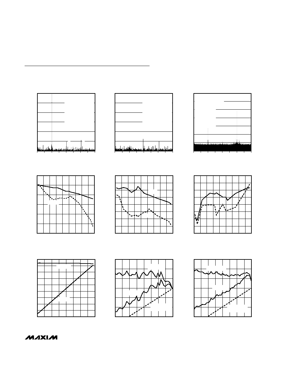
-120
-100
-80
-60
-40
-20
0
0
10
5
15
20
25
30
35
40
FFT PLOT
(32,768-POINT RECORD)
MAX19586 toc01
ANALOG INPUT FREQUENCY (MHz)
AMPLITUDE (dBFS)
f
CLK
= 80.00012288MHz
f
IN
= 10.10011317MHz
A
IN
= -2.02dBFS
SNR = 80dB
SINAD = 79.8dB
SFDR1 = 96.2dBc
SFDR2 = 101dBc
HD2 = -99.6dBc
HD3 = -96.2dBc
2
3
-120
-100
-80
-60
-40
-20
0
0
10
5
15
20
25
30
35
40
FFT PLOT
(32,768-POINT RECORD)
MAX19586 toc02
ANALOG INPUT FREQUENCY (MHz)
AMPLITUDE (dBFS)
2
3
f
CLK
= 80.00012288MHz
f
IN
= 70.16368199MHz
A
IN
= -2.06dBFS
SNR = 79.3dB
SINAD = 77.7dB
SFDR1 = 83.3dBc
SFDR2 = 98.2dBc
HD2 = -93.5dBc
HD3 = -83.3dBc
-140
-100
-120
-80
-60
-40
-20
0
0
10
5
15
20
25
30
35
40
FFT PLOT
(261,244-POINT DATA RECORD)
MAX19586 toc03
ANALOG INPUT FREQUENCY (MHz)
AMPLITUDE (dBFS)
3
2
f
CLK
= 80.00012288MHz
f
IN
= 130.00050486MHz
A
IN
= -1.82dBFS
SNR = 77.7dB
SINAD = 76.4dB
SFDR1 = 83.1dBc
SFDR2 = 91.2dBc
HD2 = -89.4dBc
HD3 = -83.1dBc
70
72
76
80
74
78
82
0
40
60
80
20
100 120 140 160 180
SNR/SINAD vs. ANALOG INPUT FREQUENCY
(f
CLK
= 80MHz, A
IN
= -2dBFS)
MAX19586toc04
f
IN
(MHz)
SNR/SINAD (dB)
SNR
SINAD
70
75
85
100
80
90
105
95
110
0
40
60
80
20
100 120 140 160 180
SFDR1/SFDR2 vs. ANALOG INPUT FREQUENCY
(f
CLK
= 80MHz, A
IN
= -2dBFS)
MAX19586toc05
f
IN
(MHz)
SFDR1/SFDR2 (dBc)
SFDR2
SFDR1
-110
-105
-95
-80
-100
-90
-75
-85
-70
0
40
60
80
20
100 120 140 160 180
HD2/HD3 vs. ANALOG INPUT FREQUENCY
(f
CLK
= 80MHz, A
IN
= -2dBFS)
MAX19586toc06
f
IN
(MHz)
HD2/HD3 (dBc)
HD3
HD2
40
50
70
60
45
55
65
75
80
85
-40
-30
-25
-20
-35
-15
-10
-5
0
SNR vs. ANALOG INPUT AMPLITUDE
(f
CLK
= 80MHz, f
IN
= 10.10011MHz)
MAX19586toc07
ANALOG INPUT AMPLITUDE (dBFS)
SNR (dB, dBFS)
SNR (dBFS)
SNR (dB)
60
80
110
90
70
100
120
-40
-30
-25
-20
-35
-15
-10
-5
0
SFDR1 vs. ANALOG INPUT AMPLITUDE
(f
CLK
= 80MHz, f
IN
= 10.10011MHz)
MAX19586toc08
ANALOG INPUT AMPLITUDE (dBFS)
SFDR1 (dBc, dBFS)
SFDR1 (dBFS)
SFDR1 (dBc)
SFDR = 90dB
REFERENCE LINE
60
80
110
90
70
100
120
-40
-30
-25
-20
-35
-15
-10
-5
0
SFDR2 vs. ANALOG INPUT AMPLITUDE
(f
CLK
= 80MHz, f
IN
= 10.10011MHz)
MAX19586toc09
ANALOG INPUT AMPLITUDE (dBFS)
SFDR2 (dBc, dBFS)
SFDR2 (dBFS)
SFDR2 (dBc)
SFDR = 90dB
REFERENCE LINE
Typical Operating Characteristics
(AV
DD
= 3.3V, DV
DD
= 1.8V, INP and INN driven differentially, internal reference, CLKP and CLKN driven differentially, C
L
= 5pF at
digital outputs, f
CLK
= 80MHz, T
A
= +25°C. Unless otherwise noted, all AC data based on 32k-point FFT records and under coherent
sampling conditions.)