MAX1955/56 DS
General Description
The MAX1955/MAX1956 are dual-output, fixed-frequency,
voltage-mode, pulse-width modulated (PWM) step-down
controllers with 0.5% output accuracy. Each controller
switches at a constant 600kHz and is 180° out-of-phase
with the other controller, reducing input ripple current
and the number of input capacitors.
An on-chip bias supply generates a 5V gate drive to
deliver up to 25A output current per phase with low-cost
N-channel MOSFETs at up to 93% efficiency. Lossless
adjustable current limit eliminates expensive current-
sense resistors and improves efficiency. Foldback current
limit reduces power dissipation during short-circuit
conditions and handles transient overloads better than
controllers using hiccup-mode short-circuit protection.
Output voltage margining shifts output voltage by
±4% from the nominal value to simplify system test.
Outputs also can be powered up and down in select-
able sequences to meet core and logic supply-rail
requirements.
The MAX1955/MAX1956 are available in a 28-lead thin
QFN package with exposed pad.
Applications
Base Stations
Telecom and Network Equipment
Servers
DSP, ASIC, µP, and FPGA Supplies
Features
o Operates from a 1.6V to 5.5V Supply (MAX1956)
o 0.5% Output Accuracy
o 0.8V to 0.9V
IN
Output Range
o Up to 25A per Phase Output Current
o On-Chip Boost Regulator Provides 5V Gate Drive
o Up to 93% Efficiency
o 180° Out-of-Phase Operation
o ±4% Voltage Margining
o Lossless, Foldback Current Limit
o Selectable Voltage Sequencing
o Synchronizable to External Clock
o Digital Soft-Start and Soft-Stop
o Small 28-Pin, 5mm
5mm Thin QFN Package
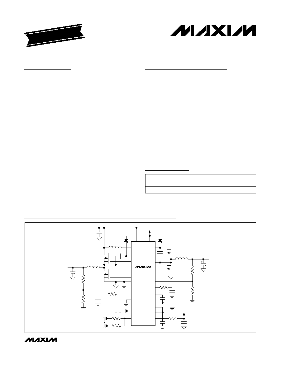
MAX1955/MAX1956
1.6V to 5.5V Input, 0.5% Accurate, Dual
180° Out-of-Phase Step-Down Controllers
________________________________________________________________ Maxim Integrated Products
1
Ordering Information
LXB
BST1
DH1
LX1
DL1
PGND
FB1
COMP1
SEQ
SYNC
SYNCHRONIZATION
CLOCK
EN
ON/OFF
VOLTAGE
MARGINING
BST2
DH2
LX2
DL2
FB2
COMP2
REF
GND
ILIM1
ILIM2
AV
DD
IN
V
DD
INPUT
1.6V TO 5.5V
OUTPUT 1
0.8V TO 0.9V
IN
UP TO 25A
OUTPUT 2
0.8V TO 0.9V
IN
UP TO 25A
VDD
VDD
MAX1956
Typical Operating Circuit
19-2623; Rev 0; 1/03
For pricing, delivery, and ordering information, please contact Maxim/Dallas Direct! at
1-888-629-4642, or visit Maxim's website at www.maxim-ic.com.
EVALUATION KIT
AVAILABLE
PART
TEMP RANGE
PIN-PACKAGE
MAX1955ETI
-40
°C to +85°C
28 Thin QFN-EP*
MAX1956ETI
-40
°C to +85°C
28 Thin QFN-EP*
*EP = Exposed pad.
Pin Configuration appears at end of data sheet.
MAX1955/MAX1956
1.6V to 5.5V Input, 0.5% Accurate, Dual
180° Out-of-Phase Step-Down Controllers
2
_______________________________________________________________________________________
ABSOLUTE MAXIMUM RATINGS
Stresses beyond those listed under "Absolute Maximum Ratings" may cause permanent damage to the device. These are stress ratings only, and functional
operation of the device at these or any other conditions beyond those indicated in the operational sections of the specifications is not implied. Exposure to
absolute maximum rating conditions for extended periods may affect device reliability.
IN, AVDD, SYNC, EN, ILIM_, FB_, SEQ to GND.......-0.3V to +6V
COMP_, REF to GND..............................-0.3V to (V
AVDD
+ 0.3V)
LXB to GND ..............................................-0.3V to (V
VDD
+ 0.3V)
DL_ to GND ...............................(V
PGND
- 0.3V) to (V
VDD
+ 0.3V)
BST_ to GND ..........................................................-0.3V to +12V
DH1 to LX1 ...............................................-0.3V to (BST1 + 0.3V)
DH2 to LX2 ...............................................-0.3V to (BST2 + 0.3V)
LX1 to BST1..............................................................-6V to +0.3V
LX2 to BST2..............................................................-6V to +0.3V
PGND to GND or VDD to AVDD ............................-0.3V to +0.3V
REF Short-Circuit to GND...........................................Continuous
I
VDD
...................................................................................250mA
Continuous Power Dissipation* (T
A
= +70°C)
28-Lead Thin QFN
(derate 20.8mW/°C above +70°C)................................1667mW
Operating Temperature Range ...........................-40°C to +85°C
Junction Temperature ......................................................+150°C
Storage Temperature Range .............................-65°C to +150°C
Lead Temperature (soldering 10s) ..................................+300°C
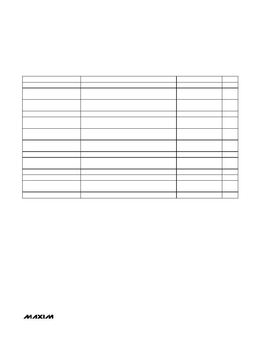
ELECTRICAL CHARACTERISTICS
(V
IN
= V
EN
= 3.3V; V
VDD
= V
AVDD
= 5V; V
PGND
= V
GND
= 0; C
REF
= 0.22µF; SEQ = SYNC = GND; T
A
= 0°C to +85°C, unless other-
wise noted. Typical values are at T
A
= +25°C.)
PARAMETER
CONDITIONS
MIN
TYP
MAX
UNITS
MAX1955
2.25
5.50
IN Input Voltage Range
MAX1956 (Note 1)
1.6
5.5
V
MAX1955, hysteresis = 35mV
1.9
2.2
IN Input Voltage UVLO
Rise or fall
MAX1956, hysteresis = 30mV
1.30
1.58
V
FB Regulation Voltage
0.796
0.8
0.804
V
FB Regulation Voltage with
Positive Voltage Margining
Percentage change from nominal regulation voltage
3
4
5
%
FB Regulation Voltage with
Negative Voltage Margining
Percentage change from nominal regulation voltage
-5
-4
-3
%
Line Regulation Error
Note 2
0.1
0.3
%
Feedback Input Bias
-0.2
+0.2
µA
Feedback Transconductance
1
2
3
mS
COMP Source Current
100
150
µA
COMP Sink Current
100
150
µA
COMP Pulldown Resistance
In shutdown
100
Output Soft-Start Time
4.27
ms
Step-Down Switching Frequency
SYNC = GND (Note 3)
540
600
660
kHz
SYNC Frequency Range
2 times step-down switching frequency
1080
1320
kHz
Maximum Duty Cycle
Measured at DH_
90
93
97
%
Minimum Duty Cycle
Measured at DH_
7
10
%
*Exposed pad soldered to PC board.
MAX1955/MAX1956
1.6V to 5.5V Input, 0.5% Accurate, Dual
180° Out-of-Phase Step-Down Controllers
_______________________________________________________________________________________
3
PARAMETER
CONDITIONS
MIN
TYP
MAX
UNITS
V
DD
No-Load Supply Current
Total of VDD1
+ VDD2 + AVDD current, SYNC = GND,
no load on DH_ or DL_
20
32
mA
IN Supply Current
35
100
µA
IN Shutdown Supply Current
20
µA
REF Voltage
1.267
1.28
1.293
V
REF Load Regulation
I
REF
= -50µA to +50µA
0.01
V
Default Current-Limit Threshold
ILIM_ = V
DD
, measured from PGND to LX_
127.5
150
172.5
mV
R
ILIM_
= 100k
60
75
90
Adjustable Current-Limit
Threshold
Measured from PGND to LX_
R
ILIM_
= 400k
240
300
360
mV
Thermal-Shutdown Threshold
T
J
rising, 15
°C hysteresis
160
°C
DH_ Gate-Driver
On-Resistance
Pulling up or down
1
1.8
DL_ Gate-Driver Pullup
On-Resistance
DL_ high state
1
1.8
DL_ Gate-Driver Pulldown
On-Resistance
DL_ low state
0.35
0.65
DH_ falling to DL_ rising
23
Dead Time (Adaptive)
DL_ falling to DH_ rising
26
ns
SYNC Minimum Pulse Width
High or low
200
ns
EN Voltage Range for Nominal
Output Voltage
Percentage of V
IN
80
90
100
%
EN Voltage Range for Positive
Voltage Margining
Percentage of V
IN
55
70
%
EN Voltage Range for Negative
Voltage Margining
Percentage of V
IN
30
45
%
EN Voltage Range for Shutdown
Percentage of V
IN
0
20
%
EN, SEQ, SYNC Input High
Voltage
(Note 4)
V
IN
- 0.5
V
SEQ, SYNC Input Low Voltage
0.5
V
EN, SEQ, SYNC Input Current
-1
+1
µA
BST_ Leakage Current in
Shutdown
-20
+20
µA
V
DD
Output Voltage
I
VDD
= 0 to 150mA
4.75
5.50
V
ELECTRICAL CHARACTERISTICS (continued)
(V
IN
= V
EN
= 3.3V; V
VDD
= V
AVDD
= 5V; V
PGND
= V
GND
= 0; C
REF
= 0.22µF; SEQ = SYNC = GND; T
A
= 0°C to +85°C, unless other-
wise noted. Typical values are at T
A
= +25°C.)
MAX1955/MAX1956
1.6V to 5.5V Input, 0.5% Accurate, Dual
180° Out-of-Phase Step-Down Controllers
4
_______________________________________________________________________________________
ELECTRICAL CHARACTERISTICS
(V
IN
= V
EN
= 3.3V; V
VDD
= V
AVDD
= 5V; PGND = GND = 0; C
REF
= 0.22µF; SYNC = GND; T
A
= -40°C to +85°C, unless otherwise
noted.) (Note 5)
PARAMETER
CONDITIONS
MIN
TYP
MAX
UNITS
MAX1955
2.25
5.50
IN Input Voltage Range
MAX1956 (Note 1)
1.6
5.5
V
MAX1955
1.9
2.2
IN Input Voltage UVLO
Rise or fall
MAX1956
1.30
1.58
V
FB Regulation Voltage
0.794
0.806
V
FB Regulation Voltage with
Positive Voltage Margining
Percentage change from nominal regulation voltage
+3
+5
%
FB Regulation Voltage with
Negative Voltage Margining
Percentage change from nominal regulation voltage
-5
-3
%
Line Regulation Error
(Note 2)
0.3
%
FB_ Input Bias
-0.2
+0.2
µA
Feedback Transconductance
1.0
3.1
mS
COMP_ Source Current
100
µA
COMP_ Sink Current
100
µA
COMP_ Pulldown Resistance
In shutdown
100
Step-Down Switching Frequency
SYNC = GND (Note 3)
540
660
kHz
SYNC Frequency Range
2 times step-down switching frequency
1080
1320
kHz
Maximum Duty Cycle
Measured at DH_
90
97
%
Minimum Duty Cycle
Measured at DH_
10
%
V
DD
Quiescent Supply Current
Total of VDD1
+ VDD2 + AVDD current, SYNC = GND,
no load on DH_ or DL_
32
mA
IN Quiescent Supply Current
100
µA
IN Shutdown Supply Current
20
µA
REF Voltage
1.267
1.293
V
REF Load Regulation
I
REF
= -50µA to +50µA
0.01
V
Default Current-Limit Threshold
ILIM_ = V
DD
; measured from PGND to LX_
127.5
172.5
mV
R
ILIM_
= 100k
60
90
Adjustable Current-Limit
Threshold
Measured from PGND to LX_
R
ILIM_
= 400k
240
360
mV
MAX1955/MAX1956
1.6V to 5.5V Input, 0.5% Accurate, Dual
180° Out-of-Phase Step-Down Controllers
_______________________________________________________________________________________
5
ELECTRICAL CHARACTERISTICS (continued)
(V
IN
= V
EN
= 3.3V; V
VDD
= V
AVDD
= 5V; PGND = GND = 0; C
REF
= 0.22µF; SYNC = GND; T
A
= -40°C to +85°C, unless otherwise
noted.) (Note 5)
PARAMETER
CONDITIONS
MIN
TYP
MAX
UNITS
DH_ Gate-Driver On-Resistance
Pulling up or down
1.8
DL_ Gate-Driver Pullup
On-Resistance
DL_ high state
1.8
DL_ Gate-Driver Pulldown
On-Resistance
DL_ low state
0.65
SYNC Minimum Pulse Width
High or low
200
ns
EN Voltage Range for Nominal
Output Voltage
Percentage of V
IN
80
100
%
EN Voltage Range for Positive
Voltage Margining
Percentage of V
IN
55
70
%
EN Voltage Range for Negative
Voltage Margining
Percentage of V
IN
30
45
%
EN Voltage Range for Shutdown
Percentage of V
IN
0
20
%
EN, SEQ, SYNC Input High
Voltage
(Note 4)
V
IN
- 0.5
V
SEQ, SYNC Input Low Voltage
0.5
V
EN, SEQ, SYNC Input Current
-1
+1
µA
BST_ Leakage Current in
Shutdown
-20
+20
µA
V
DD
Output Voltage
I
VDD
= 0 to 150mA
4.75
5.50
V
Note 1: IN input voltage must not drop below minimum voltage because of ripple or transient conditions.
Note 2: Guaranteed by design.
Note 3: Boost frequency is 2x step-down frequency.
Note 4: For proper startup, EN must exceed V
IN
- 0.5V.
Note 5: Specifications to -40°C are guaranteed by design but not production tested.