General Description
The MAX1940 triple current-limited switch with auto-
reset supplies a guaranteed 500mA load per channel in
accordance with USB specifications. The MAX1940
operates from a 4V to 5.5V input supply and consumes
only 60ÁA of quiescent current when operating and only
3ÁA in standby. Selectable active-high/active-low con-
trol logic and independent shutdown controls for each
channel provide additional flexibility. An autoreset fea-
ture latches the switch off in the event of a short circuit,
saving system power. The switch reactivates upon
removal of the shorted condition.
The MAX1940 provides several safety features to pro-
tect the USB port. Built-in thermal-overload protection
turns off the switch when the die temperature exceeds
+160░C. Accurate internal current-limiting circuitry pro-
tects the input supply against both overload and short-
circuit conditions. Independent open-drain fault signals
(FAULTA, FAULTB, and FAULTC) notify the micro-
processor when a thermal-overload, current-limit,
undervoltage lockout (UVLO), or short-circuit fault
occurs. A 20ms fault-blanking feature enables the cir-
cuit to ignore momentary faults, such as those caused
when hot-swapping a capacitive load, preventing false
alarms to the host system. The fault-blanking feature
also prevents fault signals from being issued when the
device powers up the load.
The MAX1940 is available in a space-saving 16-pin
QSOP package and operates over the extended (-40░C
to +85░C) temperature range.
Applications
Features
o Triple USB Switch in Tiny 16-Pin QSOP Package
o Autoreset Feature Saves System Power
o Guaranteed 500mA Load Current per Channel
o Built-In 20ms Fault-Blanking Circuitry
o Active-High/Active-Low Control Logic
o Fully Compliant to USB Specifications
o 4V to 5.5V Input Voltage Range
o Independent Shutdown Control
o Independent Fault Indicator Outputs
o Thermal-Overload Protection
o 3ÁA Standby Current
o UL Certification Pending
MAX1940
Triple USB Switch with Autoreset and
Fault Blanking
________________________________________________________________ Maxim Integrated Products
1
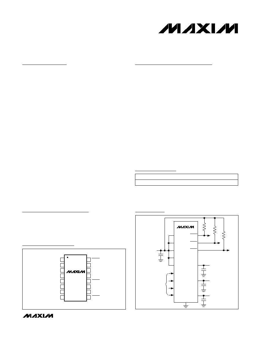
IN1
IN2
IN3
IN4
IN5
ONA
ONB
ONC
SEL
FAULTA
FAULTB
FAULTC
OUTA
OUTB
OUTC
GND
MAX1940
INPUT
4V TO 5.5V
USB
PORT A
USB
PORT B
USB
PORT C
ACTIVE-HIGH/ACTIVE-LOW
SELECTABLE
Typical Operating Circuit
Ordering Information
19-2497; Rev 0; 7/02
For pricing, delivery, and ordering information, please contact Maxim/Dallas Direct! at
1-888-629-4642, or visit Maxim's website at www.maxim-ic.com.
PART
TEMP RANGE
PIN-PACKAGE
MAX1940EEE
-40░C to +85░C
16 QSOP
16
15
14
13
12
11
10
9
1
2
3
4
5
6
7
8
ONA
FAULTA
OUTA
GND
OUTB
FAULTB
SEL
OUTC
FAULTC
TOP VIEW
MAX1940
QSOP
IN1
IN2
IN4
IN3
ONB
IN5
ONC
Pin Configuration
USB Ports
USB Hubs
Notebook Computers
Desktop Computers
PDAs and Palmtop
Computers
Docking Stations

MAX1940
Triple USB Switch with Autoreset and
Fault Blanking
2
_______________________________________________________________________________________
ABSOLUTE MAXIMUM RATINGS
Stresses beyond those listed under "Absolute Maximum Ratings" may cause permanent damage to the device. These are stress ratings only, and functional
operation of the device at these or any other conditions beyond those indicated in the operational sections of the specifications is not implied. Exposure to
absolute maximum rating conditions for extended periods may affect device reliability.
IN_, ON_, OUT_, SEL, FAULT_, to GND...................-0.3V to +6V
IN1, IN2 to OUTA......................................................-0.3V to +6V
IN2, IN3 to OUTB......................................................-0.3V to +6V
IN4, IN5 to OUTC .....................................................-0.3V to +6V
OUT_ Continuous Switch Current
(per channel, internally limited).........................................1.4A
FAULT_ DC Current ............................................................20mA
Continuous Power Dissipation (T
A
= +70░C)
16-Pin QSOP (derate 8.3mW/░C above +70░C)...........667mW
Operating Temperature Range ...........................-40░C to +85░C
Junction Temperature ......................................................+150░C
Storage Temperature Range .............................-65░C to +150░C
Lead Temperature (soldering, 10s) .................................+300░C
ELECTRICAL CHARACTERISTICS
(V
IN_
= 5V, C
IN_
= 0.1ÁF, C
OUT_
= 1ÁF, T
A
= 0░C to +85░C, unless otherwise noted. Typical values are at T
A
= +25░C.)
PARAMETER
SYM B O L
CONDITIONS
MIN
TYP
MAX
UNITS
Supply Voltage Range
V
IN_
4.0
5.5
V
Switch On-Resistance
R
ON
T
A
= 0░C to +85░C, each switch
85
135
m
Standby Supply Current
All switches disabled
3
10
ÁA
One switch enabled, I
OUT_
= 0
47
75
Two switches enabled, I
OUT_
= 0
55
90
Quiescent Supply Current
I
IN_
All switches enabled, I
OUT_
= 0
63
100
ÁA
OUT_ Off-Leakage Current
I
LKG
All switches disabled, V
OUT_
= 0,
T
A
= 0░C to +85░C
0.02
10
ÁA
Undervoltage Lockout Threshold
V
ULVO
Rising edge, 3% hysteresis
3.0
3.4
3.8
V
Continuous Load Current
500
mA
Continuous Current Limit
I
LIM
V
IN_
- V
OUT_
= 0.5V
0.7
0.9
1.2
A
0.9
1.2
1.6
A
PK
Short-Circuit Current Limit
I
SC
V
OUT_
= 0 (I
OUT_
pulsing)
0.35
A
RMS
Short-Circuit Detect Threshold
(Note 1)
1
V
Continuous Current-Limit
Blanking Timeout Period
From continuous current-limit condition to
FAULT_ asserted
10
20
35
ms
Short-Circuit Blanking Timeout
Period
From short-circuit current-limit condition to
FAULT_ asserted
7.5
18
35.0
ms
Turn-On Delay
t
ON
R
OUT_
= 10
, does not include rise time
(from ON_ to 10% of V
OUT_
)
0.5
1.2
4.0
ms
Output Rise Time
t
RISE
R
OUT_
= 10
, from 10% to 90% of V
OUT_
2.5
ms
Turn-Off Delay
t
OFF
R
OUT_
= 10
, does not include fall time
(from ON_ to 90% of V
OUT_
)
0.8
3
ms
Output Fall Time
t
FALL
R
OUT_
= 10
, from 90% to 10% of V
OUT_
2.5
ms
Thermal-Shutdown Threshold
15░C hysteresis
160
░C
ON_, SEL Input High Level
V
IH
V
IN_
= 4V to 5.5V
2
V
ON_, SEL Input Low Level
V
IL
V
IN_
= 4V to 5.5V
0.8
V
ON_, SEL Input Leakage Current
V
ON_
= 0 or V
IN_
-1
+1
ÁA
MAX1940
Triple USB Switch with Autoreset and
Fault Blanking
_______________________________________________________________________________________
3
ELECTRICAL CHARACTERISTICS (continued)
(V
IN_
= 5V, C
IN_
= 0.1ÁF, C
OUT_
= 1ÁF, T
A
= 0░C to +85░C, unless otherwise noted. Typical values are at T
A
= +25░C.)
PARAMETER
SYM B O L
CONDITIONS
MIN
TYP
MAX
UNITS
FAULT_ Output Low Voltage
V
OL
I
SINK
= 1mA, V
IN_
= 4V
0.4
V
FAULT_ Output High Leakage
Current
V
IN_
= V
FAULT_
= 5.5V
1
ÁA
OUT_ Autoreset Current
In latched off state, V
OUT_
= 0
10
25
45
mA
OUT_ Autoreset Threshold
In latched off state, OUT_ rising
0.4
0.5
0.6
V
OUT_ Autoreset Blanking Time
In latched off state, V
OUT_
> 0.5V
10
20
35
ms
ELECTRICAL CHARACTERISTICS
(V
IN_
= 5V, C
IN_
= 0.1ÁF, C
OUT_
= 1ÁF, T
A
= -40░C to +85░C, unless otherwise noted.) (Note 2)
PARAMETER
SYM B O L
CONDITIONS
MIN
MAX
UNITS
Supply Voltage Range
V
IN_
4.0
5.5
V
Switch On-Resistance
R
ON
Each switch
135
m
Standby Supply Current
All switches disabled
10
ÁA
One switch enabled, I
OUT_
= 0
75
Two switches enabled, I
OUT_
= 0
90
Quiescent Supply Current
I
IN_
All switches enabled, I
OUT_
= 0
100
ÁA
OUT_ Off-Leakage Current
I
LKG
All switches disabled, V
OUT_
= 0
10
ÁA
Undervoltage Lockout Threshold
V
ULVO
Rising edge, 3% hysteresis
3.0
3.8
V
Continuous Load Current
500
mA
Continuous Current Limit
I
LIM
V
IN_
- V
OUT_
= 0.5V
0.7
1.2
A
Short-Circuit Current Limit
I
SC
V
OUT_
= 0 (I
OUT_
pulsing)
0.9
1.6
A
PK
Continuous Current-Limit
Blanking Timeout Period
From continuous current-limit condition to
FAULT_ asserted
10
35
ms
Short-Circuit Blanking Timeout
Period
From short-circuit current-limit condition to
FAULT_ asserted
7.5
35.0
ms
Turn-On Delay
t
ON
R
OUT_
= 10
, does not include rise time
(from ON_ to 10% of V
OUT_
)
0.5
4.0
ms
Turn-Off Delay
t
OFF
R
OUT_
= 10
, does not include fall time
(from ON_ to 90% of V
OUT_
)
3
ms
ON_, SEL Input High Level
V
IH
V
IN_
= 4V to 5.5V
2
V
ON_, SEL Input Low Level
V
IL
V
IN_
= 4V to 5.5V
0.8
V
ON_, SEL Input Leakage Current
V
ON_
= 0 or V
IN_
-1
+1
ÁA
FAULT_ Output Low Voltage
V
OL
I
SINK
= 1mA, V
IN_
= 4V
0.4
V
FAULT_ Output High Leakage
Current
V
IN_
= V
FAULT_
= 5.5V
1
ÁA
OUT_ Autoreset Current
In latched off state, V
OUT_
= 0
10
50
mA
OUT_ Autoreset Threshold
In latched off state, OUT_ rising
0.4
0.6
V
OUT_ Autoreset Blanking Time
In latched off state, V
OUT_
> 0.5V
10
35
ms
Note 1: Short-circuit detect threshold is the output voltage at which the device transitions from short-circuit current limit to
continuous current limit.
Note 2: Specifications to -40░C are guaranteed by design, not production tested.
MAX1940
Triple USB Switch with Autoreset and
Fault Blanking
4
_______________________________________________________________________________________
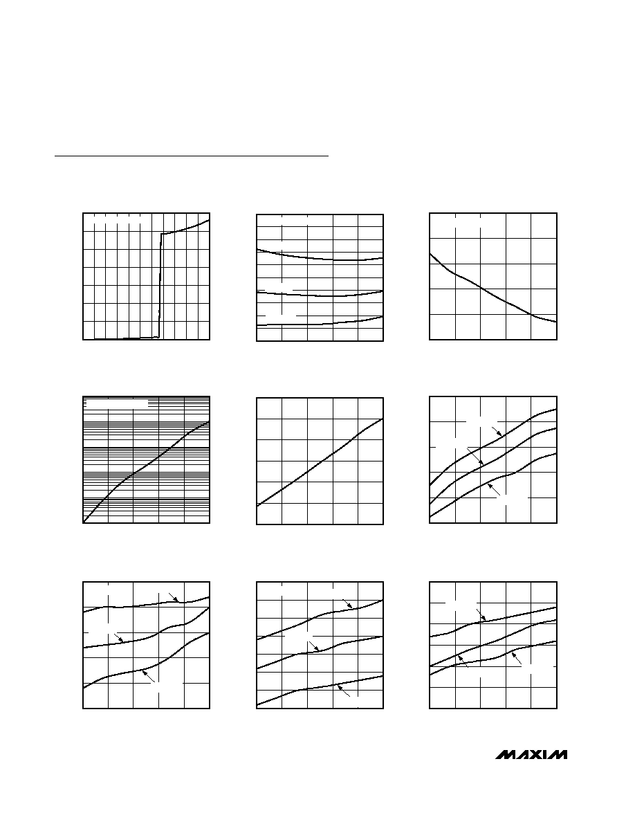
Typical Operating Characteristics
(Circuit of Figure 2, V
IN_
= 5V, C
IN_
= 0.1ÁF, C
OUT_
= 1ÁF, ON_ = SEL, T
A
= +25░C, unless otherwise noted.)
QUIESCENT SUPPLY CURRENT
vs. INPUT VOLTAGE
MAX1940 toc01
INPUT VOLTAGE (V)
QUIESCENT SUPPLY CURRENT (
Á
A)
5.0
4.5
4.0
3.5
3.0
2.5
2.0
1.5
1.0
0.5
10
20
30
40
50
60
70
0
0
5.5
ALL SWITCHES ACTIVE
QUIESCENT SUPPLY CURRENT
vs. TEMPERATURE
MAX1940 toc02
TEMPERATURE (
░C)
QUIESCENT SUPPLY CURRENT (
Á
A)
60
35
10
-15
61
62
63
64
65
66
67
68
69
70
60
-40
85
ALL SWITCHES ACTIVE
V
IN_
= 5.5V
V
IN_
= 5V
V
IN_
= 4.5V
SHUTDOWN SUPPLY CURRENT
vs. TEMPERATURE
MAX1940 toc03
TEMPERATURE (
░C)
SHUTDOWN SUPPLY CURRENT (
Á
A)
60
35
10
-15
2.6
2.7
2.8
2.9
3.0
2.5
-40
85
ON_ = GND, V
SEL
= 5V
SWITCH OFF-LEAKAGE (ONE SWITCH)
vs. TEMPERATURE
MAX1940 toc04
TEMPERATURE (
░C)
SWITCH OFF-LEAKAGE (nA)
60
35
10
-15
0.1
1
10
100
1000
0.01
-40
85
ON_ = OUT_, V
SEL
= 5V
NORMALIZED ON-RESISTANCE
vs. TEMPERATURE
MAX1940 toc05
TEMPERATURE (
░C)
NORMALIZED ON-RESISTANCE
60
35
10
-15
0.8
0.9
1.0
1.1
1.2
1.3
0.7
-40
85
CONTINUOUS CURRENT-LIMIT THRESHOLD
vs. TEMPERATURE
MAX1940 toc06
TEMPERATURE (
░C)
CONTINUOUS CURRENT-LIMIT THRESHOLD (mA)
60
35
10
-15
904
908
912
916
920
900
-40
85
V
IN_
= 5.0V
V
IN_
= 5.5V
V
IN_
= 4.5V
TURN-ON TIME (t
ON
+ t
RISE
)
vs. TEMPERATURE
MAX1940 toc07
TEMPERATURE (
░C)
TURN-ON TIME (ms)
60
35
10
-15
3.1
3.2
3.3
3.4
3.5
3.0
-40
85
V
IN_
= 5V
V
IN_
= 4.5V
V
IN_
= 5.5V
R
OUT_
= 10
MAX1940 toc08
TEMPERATURE (
░C)
TURN-OFF TIME (ms)
60
35
10
-15
2.7
2.8
2.9
3.0
3.1
3.2
3.3
2.6
-40
85
V
IN_
= 5V
V
IN_
= 5.5V
V
IN_
= 4.5V
R
OUT_
= 10
TURN-OFF TIME (t
OFF
+ t
FALL
)
vs. TEMPERATURE
FAULT-BLANKING TIME
vs. TEMPERATURE
MAX1940 toc09
TEMPERATURE (
░C)
FAULT-BLANKING TIME (ms)
60
35
10
-15
19.5
20.0
20.5
21.0
21.5
22.0
19.0
-40
85
V
IN_
= 5.5V
V
IN_
= 5V
V
IN_
= 4.5V
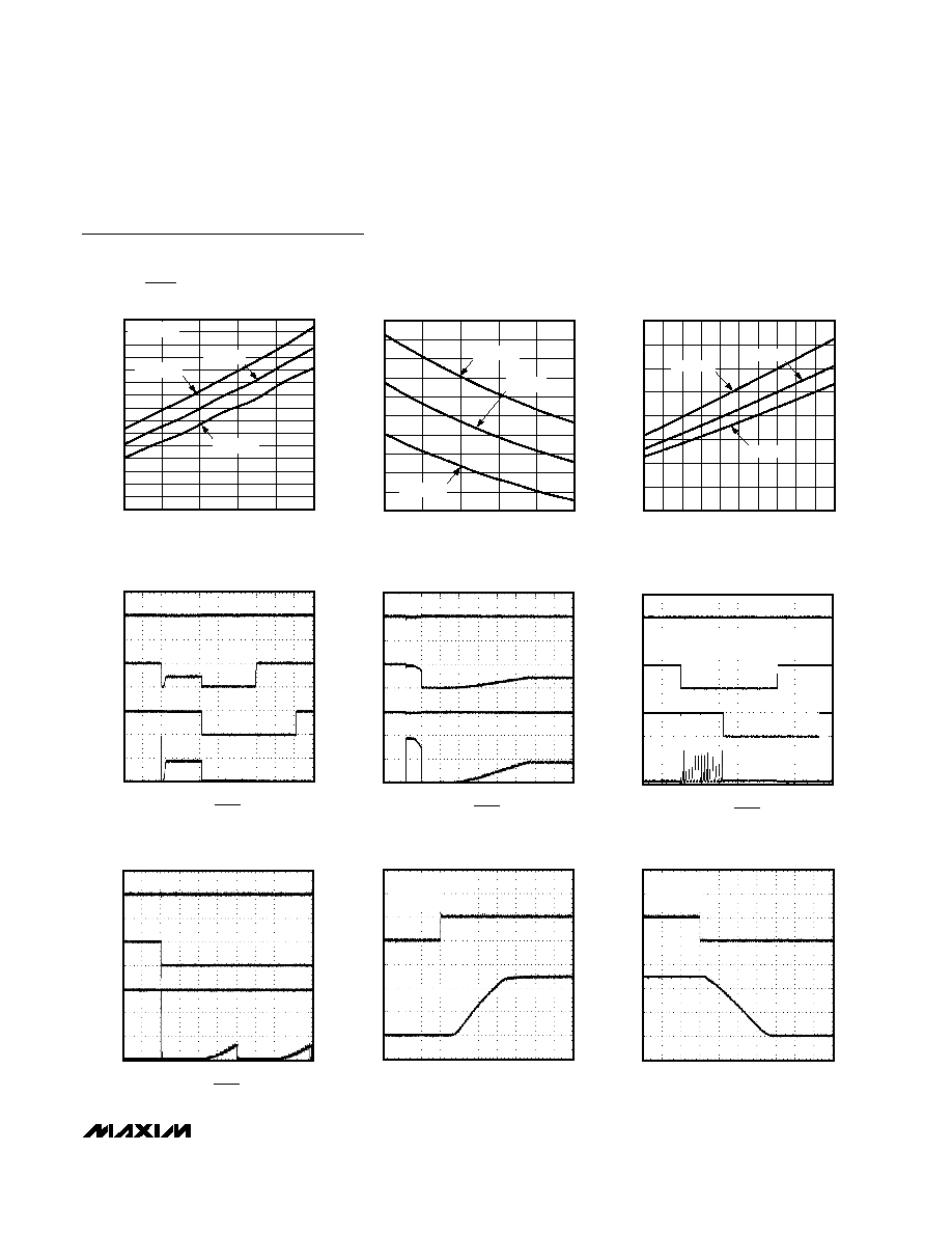
MAX1940
Triple USB Switch with Autoreset and
Fault Blanking
_______________________________________________________________________________________
5
MAX1940 toc10
TEMPERATURE (
░C)
FAULT OUTPUT LOW VOLTAGE (mV)
60
35
10
-15
110
120
130
140
150
160
170
180
190
200
210
220
230
240
250
100
-40
85
V
IN_
= 5.5V
V
IN_
= 5V
V
IN_
= 4.5V
R
PU
= 4.7k
FAULT OUTPUT LOW VOLTAGE
vs. TEMPERATURE
AUTORESET CURRENT
vs. TEMPERATURE
MAX1940 toc11
TEMPERATURE (
░C)
AUTORESET CURRENT (mA)
60
35
10
-15
20
22
24
26
28
30
32
34
36
38
18
-40
85
V
IN_
= 5.5V
V
IN_
= 4.5V
V
IN_
= 5V
AUTORESET CURRENT
vs. INPUT VOLTAGE
MAX1940 toc12
INPUT VOLTAGE (V)
AUTORESET CURRENT (mA)
5.3
5.1
3.7 3.9 4.1
4.5 4.7
4.3
4.9
5
10
15
20
25
30
35
40
0
3.5
5.5
T
A
= -40
░C
T
A
= +25
░C
T
A
= +85
░C
OVERLOAD RESPONSE INTO 2.5
MAX1940 toc13
10ms/div
B
A
C
0
5V
0
D
0
A: V
IN_
5V/div
B: V
OUT_
5V/div
C: V
FAULT_
5V/div
D: I
OUT_
1A/div
OVERLOAD RESPONSE INTO 2.5
(EXPANDED TIME SCALE)
MAX1940 toc14
400
Ás/div
B
A
C
0
5V
0
D
5V
A: V
IN_
5V/div
B: V
OUT_
5V/div
C: V
FAULT_
5V/div
D: I
OUT_
1A/div
SHORT-CIRCUIT RESPONSE INTO 0
MAX1940 toc15
10ms/div
B
A
C
5V
5V
0
D
5V
A: V
IN_
5V/div
B: V
OUT_
5V/div
C: V
FAULT_
5V/div
D: I
OUT_
1A/div
SHORT-CIRCUIT RESPONSE INTO 0
(EXPANDED TIME SCALE)
MAX1940 toc16
400
Ás/div
B
A
C
0
5V
0
D
5V
A: V
IN_
5V/div
B: V
OUT_
5V/div
C: V
FAULT_
5V/div
D: I
IN_
2A/div
MAX1940 toc17
1ms/div
B
A
5V
5V
A: V
ON_
5V/div
B: V
OUT_
2V/div
V
SEL
= 5V
R
OUT_
= 10
C
OUT_
= 1
ÁF
SWITCH TURN-ON TIME (t
ON
+ t
RISE
)
MAX1940 toc18
1ms/div
B
A
5V
0
A: V
ON_
5V/div
B: V
OUT_
2V/div
V
SEL
= 5V
R
OUT_
= 10
C
OUT_
= 1
ÁF
SWITCH TURN-ON TIME (t
ON
+ t
FALL
)
Typical Operating Characteristics (continued)
(Circuit of Figure 2, V
IN_
= 5V, C
IN_
= 0.1ÁF, C
OUT_
= 1ÁF, ON_ = SEL, T
A
= +25░C, unless otherwise noted.)