
MAX1930
Current-Limited Switch for Two USB Ports
________________________________________________________________ Maxim Integrated Products
1
OUT
1
2
8
7
OUT
OUT
IN
IN
GND
SO
TOP VIEW
3
4
6
5
MAX1930
OUTNC
EN
MAX1930
IN
OUTPUT
OUT
INPUT
2.7V TO 5.5V
ON
OFF
GND
EN
Typical Operating Circuit
19-2385; Rev 2; 11/02
Pin Configuration
Ordering Information
General Description
The MAX1930 current-limited 70m
switch with built-in
fault blanking provides an accurate, preset 1.2A to 2.3A
current limit, making it ideal for dual USB applications.
Its low quiescent supply current (16µA) and standby
current (1µA) conserve battery power in portable appli-
cations. The MAX1930 operates with inputs from 2.7V to
5.5V, making it ideal for both 3V and 5V systems.
The MAX1930 has several safety features to ensure that
the USB port is protected. Built-in thermal-overload
protection limits power dissipation and junction tempera-
ture. The device also has accurate internal current-limiting
circuitry to protect the input supply against overload.
The MAX1930 is offered in a space-saving 8-pin SO
package and operates over the extended (-40°C to
+85°C) temperature range.
Applications
Notebook Computers
USB Ports and Hubs
Docking Stations
Features
o Pin Compatible with TPS2010TPS2013
o Accurate Current Limit (1.2A min, 2.3A max)
o 125m (max) High-Side MOSFET
o Short-Circuit and Thermal Protection
o Undervoltage Lockout
o 16µA Quiescent Supply Current
o 1µA (max) Standby Supply Current
o 2.7V to 5.5V Supply Range
o UL Recognized: UL# E211395
PART
TEMP RANGE
PIN-PACKAGE
MAX1930ESA
-40°C to +85°C
8 SO
For pricing, delivery, and ordering information, please contact Maxim/Dallas Direct! at
1-888-629-4642, or visit Maxim's website at www.maxim-ic.com.
MAX1930
Current-Limited Switch for Two USB Ports
2
_______________________________________________________________________________________
ABSOLUTE MAXIMUM RATINGS
ELECTRICAL CHARACTERISTICS
(V
IN
= 5V, T
A
= 0°C to +85°C, unless otherwise noted. Typical values are at T
A
= +25°C.)
Stresses beyond those listed under "Absolute Maximum Ratings" may cause permanent damage to the device. These are stress ratings only, and functional
operation of the device at these or any other conditions beyond those indicated in the operational sections of the specifications is not implied. Exposure to
absolute maximum rating conditions for extended periods may affect device reliability.
IN, EN to GND ..........................................................-0.3V to +6V
OUT to GND ................................................-0.3V to (V
IN
+ 0.3V)
Maximum Switch Current.........................2.3A (internally limited)
OUT Short Circuit to GND ..........................................Continuous
Continuous Power Dissipation (T
A
= +70°C)
8-Pin SO (derate 5.88mW/°C above +70°C)................471mW
Operating Temperature Range (extended) .........-40°C to +85°C
Storage Temperature Range .............................-65°C to +150°C
Lead Temperature (soldering, 10s) .................................+300°C
PARAMETER
SYMBOL
CONDITIONS
MIN
TYP
MAX
UNITS
OPERATING CONDITION
Input Voltage
V
IN
2.7
5.5
V
POWER SWITCH
T
A
= +25°C
V
IN
= 4.4V to 5.5V
70
100
V
IN
= 4.4V to 5.5V
125
Switch Static Drain-Source
On-Resistance
R
DS(ON)
T
A
= 0°C to +85°C
V
IN
= 3V
72
150
m
Switch Turn-On Time
t
ON
I
LOAD
= 400mA
80
200
µs
Switch Turn-Off Time
t
OFF
I
LOAD
= 400mA
3
6
20
µs
ENABLE INPUT (EN)
V
IN
= 2.7V to 3.6V
2.0
EN High-Level Input Voltage
V
IH
V
IN
= 3.7V to 5.5V
2.4
V
EN Low-Level Input Voltage
V
IL
V
IN
= 2.7V to 5.5V
0.8
V
EN Input Current
V
EN
= V
IN
or GND
-1
+1
µA
Startup Time
V
IN
= 5V, C
OUT
= 150µF from EN driven low
to 50% full V
OUT
1
ms
CURRENT LIMIT
Overload Output Current
I
LIMIT
Force V
OUT
to 4.5V
1.2
1.75
2.3
A
Short-Circuit Output Current
I
SC
OUT shorted to GND
1
1.5
A
SUPPLY CURRENT
Supply Current, Low-Level Input
V
EN
= V
IN
= V
OUT
= 5.5V
0.002
1
µA
Timer not running
16
25
Supply Current, High-Level Input
I
Q
V
EN
= 0, I
OUT
= 0
Timer running
35
µA
T
A
= +25°C
0.01
2
Supply Leakage Current
V
EN
= V
IN
= 5.5V,
V
OUT
= 0
T
A
= 0°C to +85°C
15
µA
UNDERVOLTAGE LOCKOUT
Undervoltage Lockout
UVLO
Rising edge, 100mV hysteresis
2.0
2.4
2.6
V
THERMAL SHUTDOWN
Thermal-Shutdown Threshold
165
°C
MAX1930
Current-Limited Switch for Two USB Ports
_______________________________________________________________________________________
3
Note 1: Specifications to -40°C are guaranteed by design, not production tested.
ELECTRICAL CHARACTERISTICS
(V
IN
= 5V, T
A
= -40°C to +85°C, unless otherwise noted.) (Note 1)
PARAMETER
SYMBOL
CONDITIONS
MIN
TYP
MAX
UNITS
OPERATING CONDITION
Input Voltage
V
IN
3.0
5.5
V
POWER SWITCH
V
IN
= 4.4V to 5.5V
125
Switch Static Drain-Source
On-Resistance
R
DS(ON)
V
IN
= 3V
150
m
Switch Turn-On Time
t
ON
I
LOAD
= 400mA
200
µs
Switch Turn-Off Time
t
OFF
I
LOAD
= 400mA
1
20
µs
ENABLE INPUT (EN)
V
IN
= 3V to 3.6V
2.0
EN High-Level Input Voltage
V
IH
V
IN
= 3.7V to 5.5V
2.4
V
EN Low-Level Input Voltage
V
IL
V
IN
= 3V to 5.5V
0.8
V
EN Input Current
V
EN
= V
IN
or GND
-1
+1
µA
CURRENT LIMIT
Overload Output Current
I
LIMIT
Force V
OUT
to 4.5V
1.2
2.3
A
Short-Circuit Output Current
I
SC
OUT shorted to GND
1.5
A
SUPPLY CURRENT
Supply Current, Low-Level Input
V
EN
= V
IN
= V
OUT
= 5.5V
2
µA
Supply Current, High-Level Input
I
Q
V
EN
= GND, I
OUT
= 0, timer not running
25
µA
Supply Leakage Current
V
EN
= V
IN
= 5.5V, V
OUT
= GND
15
µA
UNDERVOLTAGE LOCKOUT
Undervoltage Lockout
UVLO
Rising edge, 100mV hysteresis
2.0
2.9
V
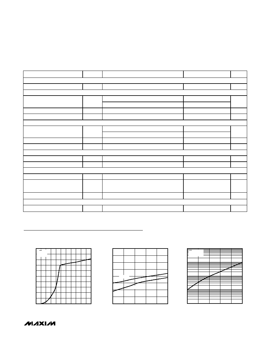
Typical Operating Characteristics
(Circuit of Figure 2, V
IN
= 5V, T
A
= +25°C, unless otherwise noted.)
0
6
4
2
8
10
12
14
16
18
20
0 0.5
2.0 2.5
1.0 1.5
3.0 3.5 4.0 4.5 5.0 5.5
QUIESCENT CURRENT vs. INPUT VOLTAGE
MAX1930 toc01
INPUT VOLTAGE (V)
QUIESCENT CURRENT (
µ
A)
I
OUT
= 0
V
EN
= 0
14.5
14.0
15.5
15.0
16.5
16.0
17.5
17.0
18.0
-40
-15
10
35
60
85
QUIESCENT CURRENT vs. TEMPERATURE
MAX1930 toc02
TEMPERATURE (
°C)
QUIESCENT CURRENT (
µ
A)
V
IN
= 5V
V
IN
= 3V
I
OUT
= 0
100
0.01
OFF SUPPLY CURRENT
vs. TEMPERATURE
0.1
1
10
MAX1930 toc03
TEMPERATURE (
°C)
OFF SUPPLY CURRENT (nA)
-40
-15
10
35
60
85
EN = IN
OUT = OPEN

0
0
0
20
µs/div
MAX1930 toc10
SWITCH TURN-ON TIME
V
OUT
, 5V/div
I
OUT
,
500mA/div
V
EN
, 5V/div
0
0
0
1
µs/div
MAX1930 toc11
SWITCH TURN-OFF TIME
V
OUT
, 5V/div
I
OUT
,
500mA/div
V
EN
, 5V/div
STARTUP TIME
(TYPICAL USB APPLICATION)
MAX1930 toc12
1ms/div
0
0
0
FULL CURRENT LIMIT CHARGES CAPACITOR
RESISTOR LOAD CURRENT
SHORT-CIRCUIT
CURRENT LIMIT
V
OUT
5V/div
V
EN
5V/div
I
IN
1A/div
MAX1930
Current-Limited Switch for Two USB Ports
4
_______________________________________________________________________________________
0
40
20
80
60
140
120
100
160
-40
-15
10
35
60
85
TURN-ON TIME vs. TEMPERATURE
MAX1930 toc07
TEMPERATURE (
°C)
TURN-ON TIME (
µ
s)
I
OUT
= 850mA
C
OUT
= 0.1
µF
V
IN
= 3V
V
IN
= 5V
4.0
5.5
6.0
5.0
4.5
7.5
7.0
6.5
8.5
8.0
9.0
-40
10
-15
35
60
85
TURN-OFF TIME vs. TEMPERATURE
MAX1930 toc08
TEMPERATURE (
°C)
TURN-OFF TIME (
µ
s)
I
OUT
= 850mA
C
OUT
= 0.1
µF
V
IN
= 3V
V
IN
= 5V
5V
0
0
4
µs/div
MAX1930 toc09
CURRENT-LIMIT RESPONSE
V
IN
AC-COUPLED
500mV/div
V
OUT
, 5V/div
I
OUT
, 2A/div
100
1000
0.01
OFF SWITCH CURRENT
vs. TEMPERATURE
0.1
1
10
MAX1930 toc04
TEMPERATURE (
°C)
OFF SWITCH CURRENT (nA)
-40
-15
10
35
60
85
EN = IN
V
OUT
= 0
-40
-15
35
85
NORMALIZED ON-RESISTANCE
vs. TEMPERATURE
MAX1930 toc05
TEMPERATURE (
°C)
NORMALIZED R
ON
10
60
0.4
0.7
0.6
0.5
0.9
0.8
1.3
1.2
1.1
1.0
1.4
I
OUT
= 850mA
0
0.4
0.2
0.8
0.6
1.0
1.2
0
0.5
2.0 2.5 3.0 3.5
1.0 1.5
4.0 4.5 5.0
NORMALIZED OUTPUT CURRENT
vs. OUTPUT VOLTAGE
MAX1930 toc06
OUTPUT VOLTAGE (V)
NORMALIZED OUTPUT CURRENT
SHORT-CIRCUIT CURRENT
I
LIMIT
(1.75A)
Typical Operating Characteristics (continued)
(Circuit of Figure 2, V
IN
= 5V, T
A
= +25°C, unless otherwise noted.)

MAX1930
Current-Limited Switch for Two USB Ports
_______________________________________________________________________________________
5
Detailed Description
The MAX1930 P-channel MOSFET power switch limits
output current to 1.2A (min) and 2.3A (max). When the
output current increases beyond the current limit
(I
LIMIT
), the current also increases through the replica
switch (I
OUT
/ 13,000). The current-limit error amplifier
compares the voltage to the internal 1.24V reference
and regulates the current back to the I
LIMIT
(Figure 1).
These switches are not bidirectional. As a result, the
input voltage must be higher than the output voltage.
Continuous Short-Circuit Protection
The MAX1930 is a short-circuit protected switch. In the
event of an output short-circuit condition, the current
through the switch is foldback-current-limited to 1A
continuous.
Thermal Shutdown
The MAX1930 has a thermal shutdown feature. The
switch turns off when the junction temperature exceeds
+165°C. When the MAX1930 cools 20°C, the switch
turns back on. If the fault short-circuit condition is not
removed, the switch cycles on and off, resulting in a
pulsed output.
Applications Information
Input Capacitor
To limit the input voltage drop during momentary output
short-circuit conditions, connect a capacitor from IN to
GND. A 1µF ceramic capacitor is adequate for most
applications; however, higher capacitor values further
reduce the voltage drop at the input (Figure 2).
Output Capacitor
Connect a 0.1µF capacitor from OUT to GND. This
capacitor helps to prevent inductive parasitics from
pulling OUT negative during turn-off.
Layout and Thermal Dissipation
It is important to optimize the switch response time to
output short-circuit conditions by keeping all traces as
short as possible to reduce the effect of undesirable
parasitic inductance. Place input and output capacitors
as close as possible to the device (no more than 5mm
away). All IN and OUT pins must be connected with
short traces to the power bus. Wide power-bus planes
provide superior heat dissipation through the
MAX1930's IN and OUT pins.
Under normal operating conditions, the package can
dissipate and channel heat away. Calculate the maxi-
mum power dissipation as follows:
P = (I
LIMIT
)
2
R
ON
where I
LIMIT
is the preset current limit (2.3A max) and
R
ON
is the on-resistance of the switch (125m
max).
When the output is short circuited, foldback-current-lim-
iting activates and the voltage drop across the switch
equals the input supply voltage. The power dissipated
across the switch increases, as does the die tempera-
Pin Description
MAX1930
P
P
P
OUT
GND
1.24V
ON
CURRENT-LIMIT
AMPLIFIER
REPLICA
AMPLIFIER
ON
EN
IN
Figure 1. Functional Diagram
PIN
NAME
FUNCTION
1
GND
Ground
2, 3
IN
Input. P-channel MOSFET source--connect all IN pins together and bypass with a 1µF capacitor to ground.
4
EN
Active-Low Switch Enable Input. A logic low turns on the switch.
5
OUTNC
No Connection. This pin is not internally connected and can be connected to OUT.
6, 7, 8
OUT
Switch Output. P-channel MOSFET drain--connect all OUT pins together and bypass with a 0.1µF capacitor
to ground.