
________________General Description
The MAX192 is a low-cost, 10-bit data-acquisition system
that combines an 8-channel multiplexer, high-bandwidth
track/hold, and serial interface with high conversion
speed and ultra-low power consumption. The device
operates with a single +5V supply. The analog inputs are
software configurable for single-ended and differential
(unipolar/bipolar) operation.
The 4-wire serial interface connects directly to SPITM,
QSPITM, and MicrowireTM devices, without using external
logic. A serial strobe output allows direct connection to
TMS320 family digital signal processors. The MAX192
uses either the internal clock or an external serial-
interface clock to perform successive approximation A/D
conversions. The serial interface can operate beyond
4MHz when the internal clock is used. The MAX192 has
an internal 4.096V reference with a drift of ±30ppm typi-
cal. A reference-buffer amplifier simplifies gain trim and
two sub-LSBs reduce quantization errors.
The MAX192 provides a hardwired SHDN pin and two
software-selectable power-down modes. Accessing the
serial interface automatically powers up the device, and
the quick turn-on time allows the MAX192 to be shut
down between conversions. By powering down
between conversions, supply current can be cut to
under 10µA at reduced sampling rates.
The MAX192 is available in 20-pin DIP and SO pack-
ages, and in a shrink-small-outline package (SSOP)
that occupies 30% less area than an 8-pin DIP. The
data format provides hardware and software compati-
bility with the MAX186/MAX188. For anti-aliasing filters,
consult the data sheets for the MAX291MAX297.
________________________Applications
Automotive
Pen-Entry Systems
Consumer Electronics
Portable Data Logging
Robotics
Battery-Powered Instruments, Battery
Management
Medical Instruments
____________________________Features
o
8-Channel Single-Ended or 4-Channel Differential
Inputs
o
Single +5V Operation
o
Low Power: 1.5mA (operating)
2µA (power-down)
o
Internal Track/Hold, 133kHz Sampling Rate
o
Internal 4.096V Reference
o
4-Wire Serial Interface is Compatible
with SPI, QSPI, Microwire, and TMS320
o
20-Pin DIP, SO, SSOP Packages
o
Pin-Compatible 12-Bit Upgrade (MAX186/MAX188)
_______________Ordering Information
MAX192
Low-Power, 8-Channel,
Serial 10-Bit ADC
________________________________________________________________ Maxim Integrated Products
1
20
19
18
17
16
15
14
13
12
11
1
2
3
4
5
6
7
8
9
10
TOP VIEW
DIP/SO/SSOP
V
DD
SCLK
CS
DIN
SSTRB
DOUT
DGND
AGND
REFADJ
VREF
SHDN
AGND
CH7
CH6
CH5
CH4
CH3
CH2
CH1
CH0
MAX192
___________________Pin Configuration
SPI and QSPI are trademarks of Motorola Corp.
Microwire is a trademark of National Semiconductor Corp.
19-0247; Rev. 1; 4/97
PART
TEMP. RANGE
MAX192ACPP
0°C to +70°C
MAX192BCPP
0°C to +70°C
MAX192ACWP
0°C to +70°C
20 Wide SO
20 Plastic DIP
20 Plastic DIP
PIN-PACKAGE
MAX192BCWP
0°C to +70°C
20 Wide SO
MAX192ACAP
0°C to +70°C
20 SSOP
MAX192BCAP
0°C to +70°C
20 SSOP
±1/2
±1
±1/2
INL (LSB)
±1
±1/2
±1
MAX192AEPP
-40°C to +85°C
20 Plastic DIP
±1/2
MAX192BEPP
-40°C to +85°C
20 Plastic DIP
±1
MAX192AEWP
-40°C to +85°C
20 Wide SO
±1/2
MAX192BEWP
-40°C to +85°C
20 Wide SO
±1
MAX192AEAP
-40°C to +85°C
20 SSOP
±1/2
MAX192BEAP
-40°C to +85°C
20 SSOP
±1
MAX192AMJP
-55°C to +125°C
20 CERDIP
±1/2
MAX192BMJP
-55°C to +125°C
20 CERDIP
±1
See last page for Typical Operating Circuit.
For free samples & the latest literature: http://www.maxim-ic.com, or phone 1-800-998-8800.
For small orders, phone 408-737-7600 ext. 3468.

MAX192
Low-Power, 8-Channel,
Serial 10-Bit ADC
2
_______________________________________________________________________________________
V
DD
to AGND........................................................... -0.3V to +6V
AGND to DGND.................................................... -0.3V to +0.3V
CH0CH7 to AGND, DGND ...................... -0.3V to (V
DD
+ 0.3V)
CH0CH7 Total Input Current.......................................... ±20mA
VREF to AGND .......................................... -0.3V to (V
DD
+ 0.3V)
REFADJ to AGND...................................... -0.3V to (V
DD
+ 0.3V)
Digital Inputs to DGND.............................. -0.3V to (V
DD
+ 0.3V)
Digital Outputs to DGND ........................... -0.3V to (V
DD
+ 0.3V)
Digital Output Sink Current .................................................25mA
Continuous Power Dissipation (T
A
= +70°C)
Plastic DIP (derate 11.11mW/°C above +70°C) ......... 889mW
SO (derate 10.00mW/°C above +70°C) ...................... 800mW
SSOP (derate 8.00mW/°C above +70°C) ................... 640mW
CERDIP (derate 11.11mW/°C above +70°C) .............. 889mW
Operating Temperature Ranges
MAX192_C_P ..................................................... 0°C to +70°C
MAX192_E_P .................................................. -40°C to +85°C
MAX192_MJP ............................................... -55°C to +125°C
Storage Temperature Range ............................ -60°C to +150°C
Lead Temperature (soldering, 10sec) ............................ +300°C
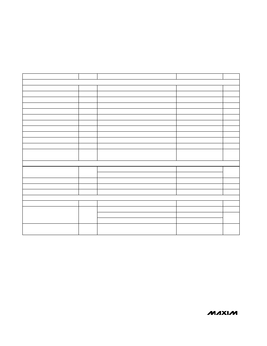
ELECTRICAL CHARACTERISTICS
(V
DD
= 5V ±5%, f
CLK
= 2.0MHz, external clock (50% duty cycle), 15 clocks/conversion cycle (133ksps), 4.7µF capacitor at VREF pin,
T
A
= T
MIN
to T
MAX,
unless otherwise noted. Typical values are at T
A
= +25°C.)
Stresses beyond those listed under "Absolute Maximum Ratings" may cause permanent damage to the device. These are stress ratings only, and functional
operation of the device at these or any other conditions beyond those indicated in the operational sections of the specifications is not implied. Exposure to
absolute maximum rating conditions for extended periods may affect device reliability.
ABSOLUTE MAXIMUM RATINGS
MAX192A
-3dB rolloff
65kHz, V
IN
= 4.096Vp-p (Note 3)
External reference, 4.096V
MAX192B
No missing codes over temperature
External reference, 4.096V
CONDITIONS
kHz
800
Full-Power Bandwidth
MHz
4.5
Small-Signal Bandwidth
dB
-75
Channel-to-Channel Crosstalk
dB
70
SFDR
Spurious-Free Dynamic Range
dB
-70
THD
Total Harmonic Distortion
(up to the 5th harmonic)
dB
66
SINAD
Signal-to-Noise + Distortion Ratio
±1/2
Bits
10
Resolution
LSB
±0.1
Channel-to-Channel
Offset Matching
ppm/°C
±0.8
Gain Temperature Coefficient
LSB
±1
Relative Accuracy (Note 2)
LSB
±1
DNL
Differential Nonlinearity
LSB
±2
Offset Error
LSB
±2
Gain Error
UNITS
MIN
TYP
MAX
SYMBOL
PARAMETER
Internal clock
5.5
10
Conversion Time (Note 4)
t
CONV
External clock, 2MHz, 12 clocks/conversion
6
µs
Track/Hold Acquisition Time
t
AZ
1.5
µs
Aperture Delay
10
ns
Aperture Jitter
<50
ps
Internal Clock Frequency
1.7
MHz
DC ACCURACY
(Note 1)
DYNAMIC SPECIFICATIONS
(10kHz sine-wave input, 4.096Vp-p, 133ksps, 2.0MHz external clock)
CONVERSION RATE

MAX192
Low-Power, 8-Channel,
Serial 10-Bit ADC
_______________________________________________________________________________________
3
ELECTRICAL CHARACTERISTICS (continued)
(V
DD
= 5V ±5%, f
CLK
= 2.0MHz, external clock (50% duty cycle), 15 clocks/conversion cycle (133ksps), 4.7µF capacitor at VREF pin,
T
A
= T
MIN
to T
MAX,
unless otherwise noted. Typical values are at T
A
= +25°C.)
Internal compensation
0mA to 0.5mA output load
T
A
= +25°C (Note 7)
(Note 5)
On/off leakage current; V
IN
= 0V, 5V
Bipolar
Used for data transfer only
Internal compensation (Note 5)
External compensation, 4.7µF
Single-ended range (unipolar only)
Common-mode range (any input)
CONDITIONS
0
mV
2.5
Load Regulation (Note 8)
ppm/°C
±30
VREF Tempco
mA
30
VREF Short-Circuit Current
V
4.066
4.096
4.126
VREF Output Voltage
pF
16
Input Capacitance
µA
±0.01
±1
Multiplexer Leakage Current
V
-V
REF
+V
REF
-2
2
Analog Input Voltage
(Note 6)
0
V
REF
0
V
REF
0
V
DD
MHz
10
External Clock Frequency
0.1
0.4
0.1
2.0
UNITS
MIN
TYP
MAX
SYMBOL
PARAMETER
Capacitive Bypass at VREF
External compensation
4.7
µF
Internal compensation
0.01
Capacitive Bypass at REFADJ
External compensation
0.01
µF
REFADJ Adjustment Range
±1.5
%
Input Voltage Range
2.5
V
DD
+
50mV
V
Input Current
200
350
µA
Input Resistance
12
20
k
Shutdown VREF Input Current
1.5
10
µA
Buffer Disable Threshold
REFADJ
V
DD
-
50mV
V
Unipolar
Differential range
Internal compensation mode
0
Capacitive Bypass at VREF
External compensation mode
4.7
µF
Reference-Buffer Gain
1.678
V/V
REFADJ Input Current
±50
µA
ANALOG INPUT
INTERNAL REFERENCE
(reference buffer enabled)
EXTERNAL REFERENCE AT VREF
(buffer disabled, VREF = 4.096V)
EXTERNAL REFERENCE AT REFADJ
Note 1:
Tested at V
DD
= 5.0V; single-ended, unipolar.
Note 2:
Relative accuracy is the deviation of the analog value at any code from its theoretical value after the full-scale range has
been calibrated.
Note 3:
Grounded on-channel; sine wave applied to all off channels.
Note 4:
Conversion time defined as the number of clock cycles times the clock period; clock has 50% duty cycle.
Note 5:
Guaranteed by design. Not subject to production testing.
Note 6:
The common-mode range for the analog inputs is from AGND to V
DD
.
Note 7:
Sample tested to 0.1% AQL.
Note 8:
External load should not change during conversion for specified accuracy.
Note 9:
Measured at V
SUPPLY
+ 5% and V
SUPPLY
- 5% only.
MAX192
Low-Power, 8-Channel,
Serial 10-Bit ADC
4
_______________________________________________________________________________________
ELECTRICAL CHARACTERISTICS (continued)
(V
DD
= 5V ±5%, f
CLK
= 2.0MHz, external clock (50% duty cycle), 15 clocks/conversion cycle (133ksps), 4.7µF capacitor at VREF pin,
T
A
= T
MIN
to T
MAX,
unless otherwise noted. Typical values are at T
A
= +25°C.)
I
SINK
= 16mA
I
SINK
= 5mA
SHDN = open
SHDN = open
SHDN = 0V
SHDN = V
DD
(Note 5)
V
IN
= 0V or V
DD
CONDITIONS
V
0.3
V
OL
Output Voltage Low
0.4
nA
-100
100
SHDN Max Allowed Leakage,
Mid Input
V
2.75
V
FLT
SHDN Voltage, Floating
V
1.5
V
DD
- 1.5
V
IM
SHDN Input Mid Voltage
µA
-4.0
I
INL
SHDN Input Current, Low
µA
4.0
I
INH
SHDN Input Current, High
V
0.5
V
INL
SHDN Input Low Voltage
V
V
DD
- 0.5
V
INH
SHDN Input High Voltage
pF
15
C
IN
DIN, SCLK, CS Input Capacitance
µA
±1
I
IN
DIN, SCLK, CS Input Leakage
V
0.15
V
HYST
DIN, SCLK, CS Input Hysteresis
V
0.8
V
INL
DIN,SCLK, CS Input Low Voltage
V
2.4
V
INH
DIN,SCLK, CS Input High Voltage
UNITS
MIN
TYP
MAX
SYMBOL
PARAMETER
Output Voltage High
V
OH
I
SOURCE
= 1mA
4
V
Three-State Leakage Current
I
L
CS = 5V
±10
µA
Three-State Leakage Capacitance
C
OUT
CS = 5V (Note 5)
15
pF
Positive Supply Voltage
V
DD
5 ±5%
V
Operating mode
1.5
2.5
mA
Fast power-down
30
70
Positive Supply Current
I
DD
Full power-down
2
10
µA
Positive Supply Rejection
(Note 9)
PSR
V
DD
= 5V ±5%; external reference, 4.096V;
full-scale input
±0.06
±0.5
mV
EXTERNAL REFERENCE AT REFADJ
DIGITAL INPUTS (DIN, SCLK,
C
--
S
,
S
--
H
--
D
--
N
)
DIGITAL OUTPUTS (DOUT, SSTRB)
POWER REQUIREMENTS
Note 5:
Guaranteed by design. Not subject to production testing.
MAX192
Low-Power, 8-Channel,
Serial 10-Bit ADC
_______________________________________________________________________________________
5
TIMING CHARACTERISTICS
(V
DD
= 5V ±5%, T
A
= T
MIN
to T
MAX
, unless otherwise noted.)
C
LOAD
= 100pF
External clock mode only, C
LOAD
= 100pF
C
LOAD
= 100pF
C
LOAD
= 100pF
C
LOAD
= 100pF
External clock mode only, C
LOAD
= 100pF
CONDITIONS
ns
200
t
STR
CS Rise to SSTRB Output
Disable (Note 5)
CS Fall to SSTRB Output Enable
(Note 5)
ns
200
t
SDV
ns
0
t
DH
DIN to SCLK Hold
ns
100
t
DS
µs
1.5
t
AZ
Acquisition Time
DIN to SCLK Setup
ns
200
t
SSTRB
SCLK Fall to SSTRB
ns
200
t
CL
SCLK Pulse Width Low
ns
200
t
CH
SCLK Pulse Width High
ns
0
t
CSH
CS to SCLK Rise Hold
ns
20
150
t
DO
ns
100
t
DV
ns
100
t
TR
SCLK Fall to Output Data Valid
ns
100
t
CSS
CS to SCLK Rise Setup
UNITS
MIN
TYP
MAX
SYMBOL
PARAMETER
SSTRB Rise to SCLK Rise
(Note 5)
t
SCK
Internal clock mode only
0
ns
CS Rise to Output Disable
CS Fall to Output Enable
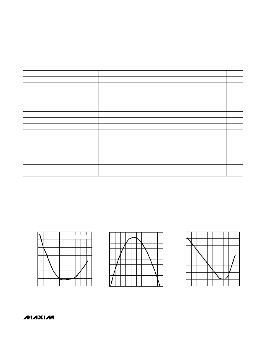
__________________________________________Typical Operating Characteristics
0.16
0
-60
-20
60
140
CHANNEL-TO-CHANNEL OFFSET MATCHING
vs. TEMPERATURE
0.02
0.12
TEMPERATURE (°C)
OFFSET MATCHING (LSBs)
20
100
0.10
0.04
-40
0
40
80
120
0.14
0.08
0.06
0.30
-0.05
-60
140
POWER-SUPPLY REJECTION
vs. TEMPERATURE
0
0.25
TEMPERATURE (°C)
PSR (LSBs)
60
0.10
0.05
-40
20
100
0.15
0.20
-20
0
40
80
120
V
DD
= +5V ±5%
2.456
INTERNAL REFERENCE VOLTAGE
vs. TEMPERATURE
2.452
2.455
TEMPERATURE (°C)
VREFADJ (V)
2.454
2.453
-40 -20 0
20 40 60 80 100 120
-60
140