_______________General Description
The MAX186/MAX188 are 12-bit data-acquisition sys-
tems that combine an 8-channel multiplexer, high-band-
width track/hold, and serial interface together with high
conversion speed and ultra-low power consumption.
The devices operate with a single +5V supply or dual
±5V supplies. The analog inputs are software config-
urable for unipolar/bipolar and single-ended/differential
operation.
The 4-wire serial interface directly connects to SPITM,
QSPITM and MicrowireTM devices without external logic. A
serial strobe output allows direct connection to TMS320
family digital signal processors. The MAX186/MAX188
use either the internal clock or an external serial-interface
clock to perform successive-approximation A/D conver-
sions. The serial interface can operate beyond 4MHz
when the internal clock is used.
The MAX186 has an internal 4.096V reference while the
MAX188 requires an external reference. Both parts
have a reference-buffer amplifier that simplifies gain
trim .
The MAX186/MAX188 provide a hard-wired
SHDN pin
and two software-selectable power-down modes.
Accessing the serial interface automatically powers up
the devices, and the quick turn-on time allows the
MAX186/MAX188 to be shut down between every
conversion. Using this technique of powering down
between conversions, supply current can be cut to
under 10µA at reduced sampling rates.
The MAX186/MAX188 are available in 20-pin DIP and
SO packages, and in a shrink small-outline package
(SSOP), that occupies 30% less area than an 8-pin DIP.
For applications that call for a parallel interface, see the
MAX180/MAX181 data sheet. For anti-aliasing filters,
consult the MAX274/MAX275 data sheet.
________________________Applications
Portable Data Logging
Data-Acquisition
High-Accuracy Process Control
Automatic Testing
Robotics
Battery-Powered Instruments
Medical Instruments
____________________________Features
o
8-Channel Single-Ended or 4-Channel
Differential Inputs
o
Single +5V or ±5V Operation
o
Low Power: 1.5mA (operating mode)
2µA (power-down mode)
o
Internal Track/Hold, 133kHz Sampling Rate
o
Internal 4.096V Reference (MAX186)
o
SPI-, QSPI-, Microwire-, TMS320-Compatible
4-Wire Serial Interface
o
Software-Configurable Unipolar or Bipolar Inputs
o
20-Pin DIP, SO, SSOP Packages
o
Evaluation Kit Available
______________Ordering Information
Ordering Information continued on last page.
NOTE: Parts are offered in grades A, B, C and D (grades defined
in Electrical Characteristics). When ordering, please specify grade.
Contact factory for availability of A-grade in SSOP package.
* Dice are specified at +25°C, DC parameters only.
* * Contact factory for availability and processing to MIL-STD-883.
TEMP. RANGE
MAX186/MAX188
Low-Power, 8-Channel,
Serial 12-Bit ADCs
________________________________________________________________ Maxim Integrated Products
1
PART
PIN-PACKAGE
MAX186_CPP
20 Plastic DIP
MAX186_CWP
20 SO
20 SSOP
MAX186DC/D
Dice*
MAX186_EPP
20 Plastic DIP
MAX186_CAP
20
19
18
17
16
15
14
13
12
11
1
2
3
4
5
6
7
8
9
10
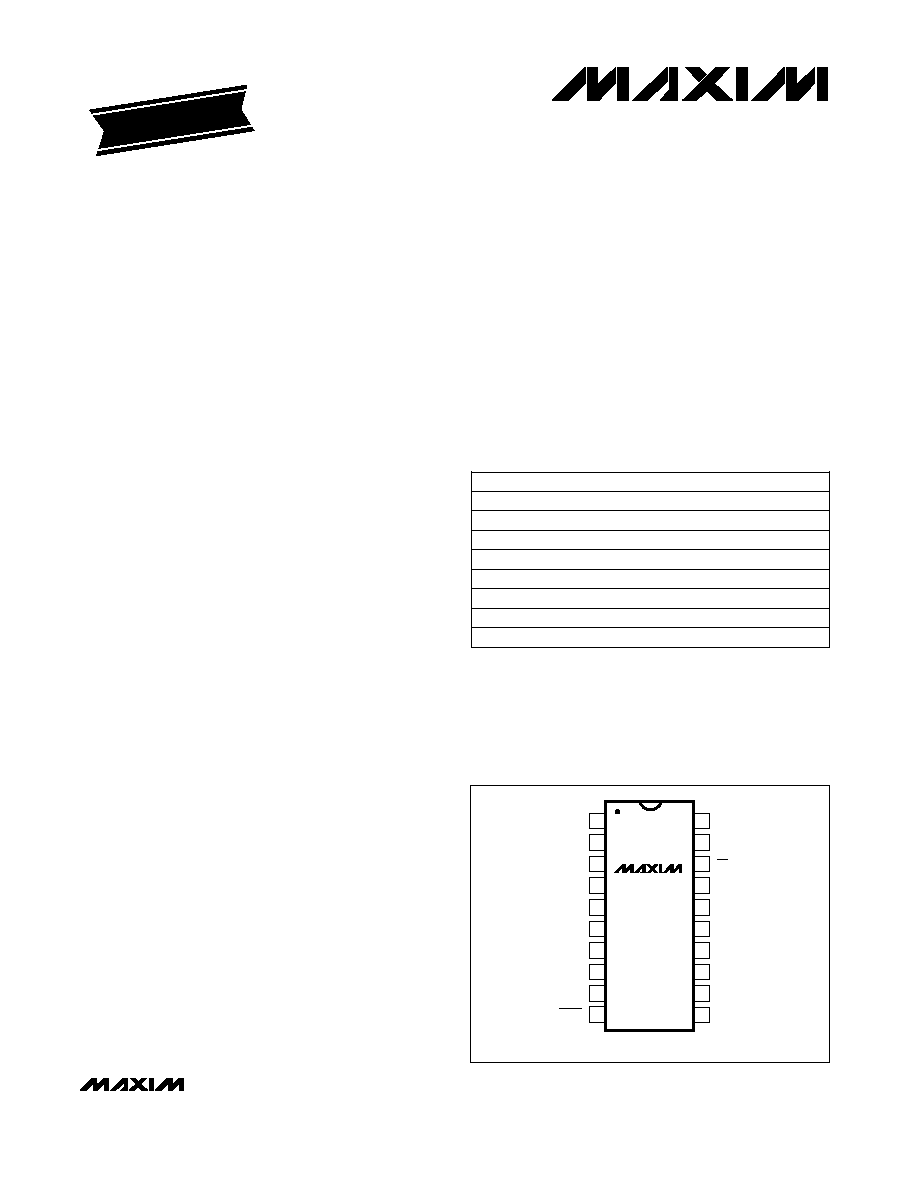
TOP VIEW
DIP/SO/SSOP
V
DD
SCLK
CS
DIN
SSTRB
DOUT
DGND
AGND
REFADJ
VREF
SHDN
V
SS
CH7
CH6
CH5
CH4
CH3
CH2
CH1
CH0
MAX186
MAX188
____________________Pin Configuration
0°C to +70°C
0°C to +70°C
0°C to +70°C
0°C to +70°C
MAX186_EWP
20 SO
MAX186_EAP
-40°C to +85°C
20 SSOP
MAX186_MJP
-55°C to +125°C
20 CERDIP**
SPI and QSPI are registered trademarks of Motorola.
Microwire is a registered trademark of National Semiconductor.
-40°C to +85°C
-40°C to +85°C
19-0123; Rev. 4; 8/96
For free samples & the latest literature: http://www.maxim-ic.com, or phone 1-800-998-8800
EVALUATION KIT
AVAILABLE

Relative Accuracy (Note 2)
MAX186/MAX188
Low-Power, 8-Channel,
Serial 12-Bit ADCs
2
_______________________________________________________________________________________
ABSOLUTE MAXIMUM RATINGS
ELECTRICAL CHARACTERISTICS
(V
DD
= 5V ±5%; V
SS
= 0V or -5V; f
CLK
= 2.0MHz, external clock (50% duty cycle); 15 clocks/conversion cycle (133ksps); MAX186--
4.7µF capacitor at VREF pin; MAX188--external reference, VREF = 4.096V applied to VREF pin; T
A
= T
MIN
to T
MAX
, unless otherwise
noted.)
Stresses beyond those listed under "Absolute Maximum Ratings" may cause permanent damage to the device. These are stress ratings only, and functional
operation of the device at these or any other conditions beyond those indicated in the operational sections of the specifications is not implied. Exposure to
absolute maximum rating conditions for extended periods may affect device reliability.
PARAMETER
SYMBOL
MIN
TYP
MAX
UNITS
±1.0
LSB
±0.75
±1.0
±0.5
Differential Nonlinearity
DNL
±1
LSB
±2.0
±3.0
±3.0
Resolution
12
Bits
±0.5
Offset Error
±3.0
LSB
±3.0
±1.5
±2.0
±2.0
Gain Error (Note 3)
±3.0
LSB
Gain Temperature Coefficient
±0.8
ppm/°C
±0.1
LSB
SINAD
70
dB
THD
-80
dB
Spurious-Free Dynamic Range
SFDR
80
dB
Channel-to-Channel Crosstalk
-85
dB
CONDITIONS
MAX186D/MAX188D
MAX186D/MAX188D
MAX186 (all grades)
MAX188C
MAX186C
MAX186B/MAX188B
No missing codes over temperature
MAX186A/MAX188A
MAX186B/MAX188B
MAX186C/MAX188C
External reference
4.096V (MAX188)
External reference, 4.096V
MAX186A/MAX188A
65kHz, V
IN
= 4.096V
P-P
(Note 4)
V
DD
to AGND............................................................-0.3V to +6V
V
SS
to AGND ............................................................+0.3V to -6V
V
DD
to V
SS
..............................................................-0.3V to +12V
AGND to DGND.....................................................-0.3V to +0.3V
CH0CH7 to AGND, DGND .............(V
SS
- 0.3V) to (V
DD
+ 0.3V)
CH0CH7 Total Input Current ..........................................±20mA
VREF to AGND ...........................................-0.3V to (V
DD
+ 0.3V)
REFADJ to AGND.......................................-0.3V to (V
DD
+ 0.3V)
Digital Inputs to DGND...............................-0.3V to (V
DD
+ 0.3V)
Digital Outputs to DGND ............................-0.3V to (V
DD
+ 0.3V)
Digital Output Sink Current .................................................25mA
Continuous Power Dissipation (T
A
= +70°C)
Plastic DIP (derate 11.11mW/°C above +70°C) ...........889mW
SO (derate 10.00mW/°C above +70°C) ........................800mW
SSOP (derate 8.00mW/°C above +70°C) .....................640mW
CERDIP (derate 11.11mW/°C above +70°C) ................889mW
Operating Temperature Ranges:
MAX186_C/MAX188_C ........................................0°C to +70°C
MAX186_E/MAX188_E......................................-40°C to +85°C
MAX186_M/MAX188_M ..................................-55°C to +125°C
Storage Temperature Range .............................-60°C to +150°C
Lead Temperature (soldering, 10sec) .............................+300°C
MAX188A
MAX188B
MAX188C
MAX188D
Channel-to-Channel
Offset Matching
Signal-to-Noise + Distortion Ratio
Total Harmonic Distortion
(up to the 5th harmonic)
DC ACCURACY
(Note 1)
DYNAMIC SPECIFICATIONS
(10kHz sine wave input, 4.096V
P-P
, 133ksps, 2.0MHz external clock, bipolar input mode)

External Clock Frequency Range
MAX186/MAX188
Low-Power, 8-Channel,
Serial 12-Bit ADCs
_______________________________________________________________________________________
3
PARAMETER
SYMBOL
CONDITIONS
MIN
TYP
MAX
UNITS
Small-Signal Bandwidth
-3dB rolloff
4.5
MHz
Full-Power Bandwidth
800
kHz
Internal clock
5.5
10
Conversion Time (Note 5)
t
CONV
External clock, 2MHz, 12 clocks/conversion
6
µs
Track/Hold Acquisition Time
t
AZ
1.5
µs
Aperture Delay
10
ns
Aperture Jitter
<50
ps
Internal Clock Frequency
1.7
MHz
ELECTRICAL CHARACTERISTICS (continued)
(V
DD
= 5V ±5%; V
SS
= 0V or -5V; f
CLK
= 2.0MHz, external clock (50% duty cycle); 15 clocks/conversion cycle (133ksps); MAX186--
4.7µF capacitor at VREF pin; MAX188--external reference, VREF = 4.096V applied to VREF pin; T
A
= T
MIN
to T
MAX
, unless otherwise
noted.)
External compensation, 4.7µF
0.1
2.0
Internal compensation (Note 6)
0.1
0.4
Used for data transfer only
10
MHz
Unipolar, V
SS
= 0V
Input Voltage Range,
Single-Ended and Differential
(Note 9)
Bipolar, V
SS
= -5V
V
Multiplexer Leakage Current
On/off leakage current, V
IN
= ±5V
±0.01
±1
µA
Input Capacitance
(Note 6)
16
pF
VREF Output Voltage
T
A
= +25°C
4.076
4.096
4.116
V
VREF Short-Circuit Current
30
mA
MAX186A, MAX186B,
MAX186C
±30
±50
±30
±60
±30
±80
VREF Tempco
MAX186D
±30
ppm/°C
Load Regulation (Note 7)
0mA to 0.5mA output load
2.5
mV
Internal compensation
0
Capacitive Bypass at VREF
External compensation
4.7
µF
Internal compensation
0.01
Capacitive Bypass at REFADJ
External compensation
0.01
µF
MAX186_C
MAX186_E
MAX186_M
REFADJ Adjustment Range
±1.5
%
±VREF/2
0 to
VREF
Input Voltage Range
V
Input Current
200
350
µA
Input Resistance
12
20
k
Shutdown VREF Input Current
1.5
10
µA
Buffer Disable Threshold REFADJ
V
DD
-
50mV
V
V
DD +
2.50
50mV
CONVERSION RATE
ANALOG INPUT
INTERNAL REFERENCE
(MAX186 only, reference buffer enabled)
EXTERNAL REFERENCE AT VREF
(Buffer disabled, VREF = 4.096V)

MAX186/MAX188
Low-Power, 8-Channel,
Serial 12-Bit ADCs
4
_______________________________________________________________________________________
ELECTRICAL CHARACTERISTICS (continued)
(V
DD
= 5V ±5%; V
SS
= 0V or -5V; f
CLK
= 2.0MHz, external clock (50% duty cycle); 15 clocks/conversion cycle (133ksps); MAX186--
4.7µF capacitor at VREF pin; MAX188--external reference, VREF = 4.096V applied to VREF pin; T
A
= T
MIN
to T
MAX
, unless otherwise
noted.)
PARAMETER
SYMBOL
CONDITIONS
MIN
TYP
MAX
Internal compensation mode
0
µF
Capacitive Bypass at VREF
External compensation mode
4.7
MAX186
1.678
V/V
MAX188
1.638
MAX186
±50
µA
REFADJ Input Current
MAX188
±5
V
INH
2.4
V
V
INL
0.8
V
DIN, SCLK,
CS Input Hysteresis
V
HYST
0.15
V
DIN, SCLK,
CS Input Leakage
I
IN
V
IN
= 0V or V
DD
±1
µA
C
IN
(Note 6)
15
pF
SHDN Input High Voltage
V
INH
V
DD
- 0.5
V
SHDN Input Low Voltage
V
INL
0.5
V
SHDN Input Current, High
I
INH
SHDN = V
DD
4.0
µA
SHDN Input Current, Low
I
INL
SHDN = 0V
-4.0
µA
SHDN Input Mid Voltage
V
IM
V
SHDN Voltage, Floating
V
FLT
SHDN = open
2.75
V
SHDN = open
-100
100
nA
I
SINK
= 5mA
0.4
Output Voltage Low
V
OL
I
SINK
= 16mA
0.3
V
Output Voltage High
V
OH
I
SOURCE
= 1mA
4
V
Three-State Leakage Current
I
L
CS = 5V
±10
µA
Three-State Output Capacitance
C
OUT
CS = 5V (Note 6)
15
pF
Positive Supply Voltage
V
DD
5 ±5%
V
DIN, SCLK,
CS Input Capacitance
SHDN Max Allowed Leakage,
Mid Input
Negative Supply Voltage
V
SS
0 or
-5 ±5%
V
Operating mode
1.5
2.5
Fast power-down
30
70
Positive Supply Current
I
DD
Full power-down
2
10
Operating mode and fast power-down
50
Negative Supply Current
I
SS
Full power-down
10
µA
mA
µA
DIN, SCLK,
CS Input Low Voltage
DIN, SCLK,
CS Input High Voltage
1.5
V
DD
-1.5
DIGITAL INPUTS (DIN, SCLK,
CS
,
SHDN
)
DIGITAL OUTPUTS (DOUT, SSTRB)
POWER REQUIREMENTS
UNITS
EXTERNAL REFERENCE AT REFADJ
Reference-Buffer Gain

Note 1:
Tested at V
DD
= 5.0V; V
SS
= 0V; unipolar input mode.
Note 2:
Relative accuracy is the deviation of the analog value at any code from its theoretical value after the full-scale range has
been calibrated.
Note 3:
MAX186 internal reference, offset nulled; MAX188 external reference (VREF = +4.096V), offset nulled.
Note 4:
Ground on-channel; sine wave applied to all off channels.
Note 5:
Conversion time defined as the number of clock cycles times the clock period; clock has 50% duty cycle.
Note 6:
Guaranteed by design. Not subject to production testing.
Note 7:
External load should not change during conversion for specified accuracy.
Note 8:
Measured at V
SUPPLY
+5% and V
SUPPLY
-5% only.
Note 9:
The common-mode range for the analog inputs is from V
SS
to V
DD
.
MAX186/MAX188
Low-Power, 8-Channel,
Serial 12-Bit ADCs
_______________________________________________________________________________________
5
PARAMETER
SYMBOL
CONDITIONS
UNITS
Positive Supply Rejection
(Note 8)
PSR
±0.06
±0.5
mV
Negative Supply Rejection
(Note 8)
PSR
V
SS
= -5V ±5%; external reference, 4.096V;
full-scale input
±0.01
±0.5
mV
ELECTRICAL CHARACTERISTICS (continued)
(V
DD
= 5V ±5%; V
SS
= 0V or -5V; f
CLK
= 2.0MHz, external clock (50% duty cycle); 15 clocks/conversion cycle (133ksps); MAX186--
4.7µF capacitor at VREF pin; MAX188--external reference, VREF = 4.096V applied to VREF pin; T
A
= T
MIN
to T
MAX
, unless otherwise
noted.)
TIMING CHARACTERISTICS
(V
DD
= 5V ±5%; V
SS
=0V or -5V, T
A
= T
MIN
to T
MAX
, unless otherwise noted.)
PARAMETER
SYMBOL
CONDITIONS
UNITS
SCLK Pulse Width Low
t
CL
200
ns
SCLK Fall to SSTRB
t
SSTRB
C
LOAD
= 100pF
200
ns
t
SDV
External clock mode only, C
LOAD
= 100pF
200
ns
t
STR
External clock mode only, C
LOAD
= 100pF
200
ns
t
SCK
Internal clock mode only
0
ns
Acquisition Time
t
AZ
1.5
µs
DIN to SCLK Setup
t
DS
100
ns
DIN to SCLK Hold
t
DH
0
ns
C
LOAD
= 100pF
20
150
ns
SCLK Fall to Output Data Valid
t
DO
20
200
ns
CS Fall to Output Enable
t
DV
C
LOAD
= 100pF
100
ns
CS Rise to Output Disable
t
TR
C
LOAD
= 100pF
100
ns
CS to SCLK Rise Setup
t
CSS
100
ns
CS to SCLK Rise Hold
t
CSH
0
ns
SCLK Pulse Width High
t
CH
200
ns
MAX18_ _C/E
MAX18_ _M
SSTRB Rise to SCLK Rise
(Note 6)
CS Fall to SSTRB Output Enable
(Note 6)
V
DD
= 5V ±5%; external reference, 4.096V;
full-scale input
MIN
TYP
MAX
MIN
TYP
MAX
CS Rise to SSTRB Output Disable
(Note 6)