
General Description
The MAX1857 low-dropout linear regulator operates
from a +2.5V to +5.5V supply and delivers a guaran-
teed 500mA load current with low 120mV dropout. The
high-accuracy (±1%) output voltage is preset at an
internally trimmed 4.75V or can be adjusted from 1.25V
to 5.0V with an external resistive divider.
An internal PMOS pass transistor allows the low 135µA
supply current to remain independent of load, making
this device ideal for portable battery-operated equip-
ment such as personal digital assistants (PDAs), cellu-
lar phones, cordless phones, base stations, and
notebook computers.
Other features include an active-low open-drain reset
output with a 4.5ms timeout period that indicates when
the output is out of regulation, a 0.1µA shutdown mode,
short-circuit protection, and thermal shutdown protec-
tion. The device is available in a miniature 8-pin µMAX
package. For higher power applications, refer to the
MAX1792 and MAX1793 data sheets.
________________________Applications
Notebook Computers
Cellular and Cordless Telephones
PDAs
Palmtop Computers
Base Stations
USB Hubs
Docking Stations
Features
o Guaranteed 500mA Output Current
o Low 120mV Dropout at 500mA
o Up to ±1% Output Voltage Accuracy
Preset at 4.75V
Adjustable from 1.25V to 5.0V
o Reset Output with 4.5ms Timeout Period
o Low 135µA Ground Current
o 0.1µA Shutdown Current
o Thermal Overload Protection
o Output Current Limit
o Tiny µMAX Package
MAX1857
500mA, Low-Dropout,
Ripple-Rejecting LDO in µMAX
________________________________________________________________ Maxim Integrated Products
1
SET
GND
SHDN
1
2
8
7
OUT
OUT
IN
RST
IN
µMAX
TOP VIEW
3
4
6
5
MAX1857
Pin Configuration
NC
MAX1857
IN
IN
ON
OFF
C
IN
1
µF
SHDN
OUT
OUT
RST
GND
SET
C
OUT
3.3
µF
TO
µC
V
IN
= +5V
V
OUT
= 4.75V
R
RST
100k
Typical Operating Circuit
19-1812; Rev 0; 1/01
Ordering Information
PART*
TEMP. RANGE
PIN-PACKAGE
MAX1857EUA47
-40
°C to +85°C
8
µMAX
*Contact factory for other preset output voltages.
For price, delivery, and to place orders, please contact Maxim Distribution at 1-888-629-4642,
or visit Maxim's website at www.maxim-ic.com.

MAX1857
500mA, Low-Dropout,
Ripple-Rejecting LDO in µMAX
2
_______________________________________________________________________________________
ABSOLUTE MAXIMUM RATINGS
ELECTRICAL CHARACTERISTICS
(V
IN
= +5.25V, V
OUT
= 4.75V, SHDN = IN, SET = GND, T
A
= 0°C to +85°C, unless otherwise noted. Typical values are at T
A
= +25°C.)
Stresses beyond those listed under "Absolute Maximum Ratings" may cause permanent damage to the device. These are stress ratings only, and functional
operation of the device at these or any other conditions beyond those indicated in the operational sections of the specifications is not implied. Exposure to
absolute maximum rating conditions for extended periods may affect device reliability.
IN, SHDN, RST, SET to GND ....................................-0.3V to +6V
OUT to GND ................................................-0.3V to (V
IN
+ 0.3V)
Output Short-Circuit Duration ........................................Indefinite
Continuous Power Dissipation (T
A
= +70°C)
8-Pin µMAX (derate 4.5mW/°C above +70°C) .............362mW
Operating Temperature Range ...........................-40°C to +85°C
Junction Temperature ......................................................+150°C
Storage Temperature Range .............................-65°C to +150°C
Lead Temperature (soldering, 10s) .................................+300°C
PARAMETER
SYMBOL
CONDITIONS
MIN
TYP
MAX
UNITS
Input Voltage
V
IN
2.5
5.5
V
Input Undervoltage Lockout
V
UVLO
Rising, 75mV hysteresis
2.0
2.15
2.3
V
V
OUT
2.5V
-1
+1
I
OUT
= 100mA,
T
A
= +85
°C
V
OUT
< 2.5V
-1.5
+1.5
%
I
OUT
= 100mA, T
A
= 0
°C to +85°C
-2
+2
Output Voltage Accuracy
(Preset Mode)
V
OUT
I
OUT
= 1mA to 500mA, V
IN
> V
OUT
+ 0.5V,
T
A
= 0
°C to +85°C
-3
+3
%
Adjustable Output Voltage
Range
V
SET
= 1.25V
1.25
5
V
T
A
= +85
°C
1.229
1.250
1.271
SET Voltage Threshold
(Adjustable Mode)
V
SET
V
IN
= +2.7V,
V
OUT
set to 2.0V,
I
OUT
= 100mA
T
A
= 0
°C to +85°C
1.219
1.281
V
Maximum Output Current
I
OUT
V
IN
2.7V
500
mA
RMS
Short-Circuit Current Limit
I
LIM
V
OUT
= 0, V
IN
2.7V
0.55
1.2
2.2
A
In-Regulation Current Limit
V
OUT
> 96% of nominal value, V
IN
2.7V
2.0
A
SET Dual ModeTM Threshold
50
100
150
mV
SET Input Bias Current
I
SET
V
SET
= 1.25V
-100
+100
nA
I
OUT
= 1mA
135
250
Ground-Pin Current
I
Q
I
OUT
= 500mA
175
µA
Dropout Voltage (Note 1)
V
IN
-
V
OUT
I
OUT
= 500mA
120
175
mV
Line Regulation
V
LNR
V
IN
from (V
OUT
+ 100mV) to 5.5V,
I
LOAD
= 5mA
-0.15
0
+0.15
%/V
Load Regulation
V
LDR
I
OUT
= 1mA to 500mA
0.4
1.0
%
Output Voltage Noise
10Hz to 1MHz, C
OUT
= 3.3
µF (ESR < 0.1)
115
µV
RMS
SHUTDOWN
Shutdown Supply Current
I
OFF
SHDN = GND, V
IN
= 5.5V
0.1
15
µA
V
IH
2.5V < V
IN
< 5.5V
1.6
SHDN Input Threshold
V
IL
2.5V < V
IN
< 5.5V
0.6
V
SHDN Input Bias Current
SHDN = IN or GND
10
100
nA
Dual Mode is a trademark of Maxim Integrated Products.

MAX1857
500mA, Low-Dropout,
Ripple-Rejecting LDO in µMAX
_______________________________________________________________________________________
3
ELECTRICAL CHARACTERISTICS
(V
IN
= +5.25V, V
OUT
= 4.75V, SHDN = IN, SET = GND, T
A
= -40°C to +85°C, unless otherwise noted.) (Note 2)
ELECTRICAL CHARACTERISTICS (continued)
((V
IN
= +5.25V, V
OUT
= 4.75V, SHDN = IN, SET = GND, T
A
= 0°C to +85°C, unless otherwise noted. Typical values are at T
A
= +25°C.)
PARAMETER
SYMBOL
CONDITIONS
MIN
TYP
MAX
UNITS
RESET OUTPUT
Reset Output Low Voltage
V
OL
RST sinking 1mA
0.01
0.1
V
Operating Voltage Range for
Valid Reset
RST sinking 100
µA
1.0
5.5
V
RST Output High Leakage
Current
V
RST
= +5.5V
100
nA
RST Threshold
Rising edge, referred to V
OUT(NOMINAL)
83
86
89
%
RST Release Delay
t
RP
Rising edge of OUT to rising edge of
RST
1.4
4.5
8
ms
THERMAL PROTECTION
Ther m al S hutd ow n Tem p er atur e
T
SHDN
170
°C
Thermal Shutdown Hysteresis
T
SHDN
20
°C
PARAMETER
SYMBOL
CONDITIONS
MIN
MAX
UNITS
Input Voltage
V
IN
2.5
5.5
V
Input Undervoltage Lockout
V
UVLO
Rising or falling
2.0
2.3
V
Output Voltage Accuracy
(Preset Mode)
V
OUT
I
OUT
= 1mA to 500mA
-3
+3
%
Adjustable Output Voltage
Range
V
SET
= 1.25V
1.25
5
V
SET Voltage Threshold
(Adjustable Mode)
V
SET
I
OUT
= 100mA
1.212
1.288
V
Maximum Output Current
I
OUT
500
mA
RMS
Short-Circuit Current Limit
I
LIM
V
OUT
= 0
0.55
2.2
A
SET Dual Mode Threshold
50
150
mV
SET Input Bias Current
I
SET
V
SET
= 1.25V
-100
+100
nA
Ground-Pin Current
I
Q
I
OUT
= 1mA
250
µA
Dropout Voltage (Note 1)
V
IN
-
V
OUT
I
OUT
= 500mA
175
mV
Line Regulation
V
LNR
V
IN
from (V
OUT
+ 100mV) to 5.5V,
I
LOAD
= 5mA
-0.15
+0.15
%/V
Load Regulation
V
LDR
I
OUT
= 1mA to 500mA
1.0
%
SHUTDOWN
Shutdown Supply Current
I
OFF
SHDN = GND, V
IN
= +5.5V
15
µA
V
IH
2.5V < V
IN
< 5.5V
1.6
SHDN Input
Threshold
V
IL
2.5V < V
IN
< 5.5V
0.6
V
SHDN Input Bias Current
SHDN = IN or GND
100
nA

4.64
4.68
4.76
4.72
4.80
0
200
400
600
800
1000
OUTPUT VOLTAGE
vs. OUTPUT CURRENT
MAX1857 toc01
OUTPUT CURRENT (mA)
OUTPUT VOLTAGE (V)
V
IN
= 5.25V
V
IN
= 5.00V
4.70
4.72
4.76
4.74
4.78
4.80
-55
5
-25
35
65
95
125
OUTPUT VOLTAGE vs. TEMPERATURE
MAX1857 toc02
TEMPERATURE (
°C)
OUTPUT VOLTAGE (V)
I
OUT
= 0mA
0
150
100
50
200
250
300
0
400
200
600
800
1000
DROPOUT VOLTAGE
vs. OUTPUT CURRENT
MAX1857 toc03
OUTPUT CURRENT (mA)
DROPOUT VOLTAGE (mV)
T
A
= +25
°C
T
A
= -40
°C
T
A
= +85
°C
Typical Operating Characteristics
(V
IN
= +5.25V, V
OUT
= 4.75V, SHDN = IN, SET = GND, C
IN
= 1µF, C
OUT
= 3.3µF, T
A
= +25°C, unless otherwise noted.)
MAX1857
500mA, Low-Dropout,
Ripple-Rejecting LDO in µMAX
4
_______________________________________________________________________________________
PARAMETER
SYMBOL
CONDITIONS
MIN
MAX
UNITS
RESET OUTPUT
Reset Output Low Voltage
V
OL
RST sinking 1mA
0.1
V
Operating Voltage Range for
Valid Reset
RST sinking 100
µA
1.0
5.5
V
RST Output High Leakage
Current
V
RST
= +5.5V
100
nA
RST Threshold
Rising edge, referred to V
OUT(NOMINAL)
83
89
%
RST Release Delay
t
RP
Rising edge of OUT to rising edge of
RST
1.4
8
ms
ELECTRICAL CHARACTERISTICS (continued)
(V
IN
= +5.25V, V
OUT
= 4.75V, SHDN = IN, SET = GND, T
A
= -40°C to +85°C, unless otherwise noted.) (Note 2)
Note 1: Dropout voltage is defined as V
IN
- V
OUT
, when V
OUT
is 100mV below the value of V
OUT
measured when V
IN
= V
OUT(NOM)
+ 0.5V. Since the minimum input voltage is 2.5V, this specification is only meaningful when V
OUT(NOM)
2.5V. For V
OUT(NOM)
between 2.5V and 3.5V, use the following equations: Typical Dropout = -93mV/V
V
OUT(NOM)
+ 445mV; Guaranteed Maximum
Dropout = -137mV/V
V
OUT(NOM)
+ 704mV. For V
OUT(NOM)
3.5V: Typical Dropout = 120mV; Guaranteed Maximum Dropout
= 175mV.
Note 2: Specifications to -40°C are guaranteed by design, not production tested.
MAX1857
500mA, Low-Dropout,
Ripple-Rejecting LDO in µMAX
_______________________________________________________________________________________
5
80
70
60
50
40
30
20
10
0
0.01
1
10
0.1
100
POWER-SUPPLY REJECTION RATIO
vs. FREQUENCY
MAX1857 toc04
FREQUENCY (kHz)
PSRR (dB)
1000
C
OUT
= 3.3
µF
I
OUT
= 50mA
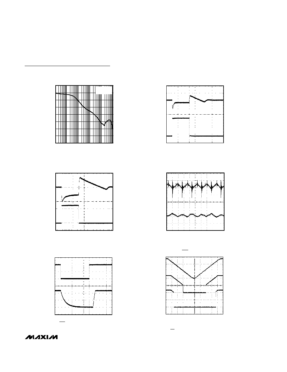
LOAD-TRANSIENT RESPONSE
MAX1857 toc05
10
µs/div
4.80V
0
600mA
4.75V
4.70V
400mA
200mA
A: V
OUT
= 4.75V, 50mV/div
B: I
OUT
= 5mA TO 500mA, 200mA/div
V
IN
= 5.25V, C
IN
= 10
µF
A
B
LOAD-TRANSIENT RESPONSE
NEAR DROPOUT
MAX1857 toc06
10
µs/div
0
4.80V
4.75V
4.70V
4.65V
400mA
200mA
A: V
OUT
= 4.75V, 50mV/div
B: I
OUT
= 5mA TO 500mA, 200mA/div
V
IN
= V
OUT
+ 100mV = 4.85V, C
IN
= 10
µF
A
B
SWITCHING POWER-SUPPLY
RIPPLE REJECTION
MAX1857 toc07
2
µs/div
5.0V
4.75V
A: MAX1632: V
IN
= 9V, V
OUT
= 5.0V, 20mV/div
B: MAX1857: V
OUT
= 4.75V, I
OUT
= 500mA, 2mV/div
OUT
MAX1632
= IN
MAX1857
A
B
RST WAVEFORM
MAX1857 toc09
20ms/div
A: V
IN
= 0 TO 5.5V, 2V/div
B: V
OUT
= 4.75V, R
OUT
= 95
, 2V/div
C: V
RST
, 100k
TO OUT, 2V/div
A
B
0
0
0
C
Typical Operating Characteristics (continued)
(V
IN
= +5.25V, V
OUT
= 4.75V, SHDN = IN, SET = GND, C
IN
= 1µF, C
OUT
= 3.3µF, T
A
= +25°C, unless otherwise noted.)
SHUTDOWN WAVEFORM
MAX1857 toc08
40
µs/div
6V
2V
A: V
SHDN
= 0 TO 2V, 1V/div
B: V
OUT
= 4.75V, 2V/div
R
OUT
= 9.5
(500mA)
A
B
2V
1V
0
4V
0