Äîêóìåíòàöèÿ è îïèñàíèÿ www.docs.chipfind.ru
_______________General Description
The MAX1822 high-side supply, using a regulated
charge pump, generates a regulated output voltage
11V greater than the input supply voltage to power
high-side switching and control circuits. The MAX1822
allows low-resistance N-channel MOSFETs (FETs) to be
used in circuits that normally require costly, less effi-
cient P-channel FETs and PNP transistors. The high-
side output also eliminates the need for logic FETs in
+5V and other low-voltage switching circuits.
A +3.5V to +16.5V input supply range and a typical qui-
escent current of only 150µA make the MAX1822 ideal
for a wide range of line- and battery-powered switching
and control applications where efficiency is crucial.
Also provided is a logic-level power-ready output (PR)
to indicate when the high-side voltage reaches the
proper level.
The MAX1822 comes in an 8-pin SO package and
requires three inexpensive external capacitors. The
MAX1822 is a pin-for-pin replacement to the MAX622.
________________________Applications
High-Side Power Control with N-Channel FETs
Low-Dropout Voltage Regulators
Power Switching from Low Supply Voltages
H-Switches
Stepper Motor Drivers
Battery-Load Management
Portable Computers
____________________________Features
o +3.5V to +16.5V Operating Supply Voltage Range
o Output Voltage Regulated to V
CC
+ 11V (typ)
o 150µA (typ) Quiescent Current
o Power-Ready Output
MAX1822
High-Side Power Supply
________________________________________________________________ Maxim Integrated Products
1
C2+
V
OUT
GND
1
2
8
7
V
CC
C1-
C2-
PR
C1+
SO
TOP VIEW
3
4
6
5
MAX1822
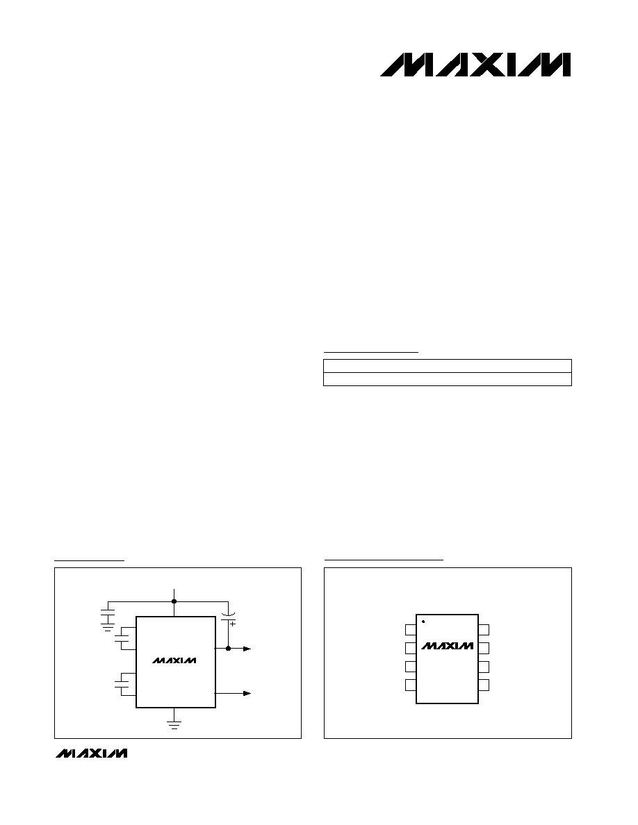
Pin Configuration
MAX1822
+3.5V TO +16.5V
0.1
µF
CERAMIC
GND
+12.5V TO +27.5V
1
8
5
3
PR
V
OUT
V
CC
7
C1
C3
4
C1+
C1-
C2+
C2-
6
2
C2
Typical Operating Circuit
19-1892; Rev 0; 1/01
PART
MAX1822ESA
-40°C to +85°C
TEMP. RANGE
PIN-PACKAGE
8 SO
Ordering Information
For price, delivery, and to place orders, please contact Maxim Distribution at 1-888-629-4642,
or visit Maxim's website at www.maxim-ic.com.
MAX1822
High-Side Power Supply
2
_______________________________________________________________________________________
ABSOLUTE MAXIMUM RATINGS
ELECTRICAL CHARACTERISTICS
(V
CC
= +5V, T
A
= T
MIN
to T
MAX
, unless otherwise noted.)
Stresses beyond those listed under "Absolute Maximum Ratings" may cause permanent damage to the device. These are stress ratings only, and functional
operation of the device at these or any other conditions beyond those indicated in the operational sections of the specifications is not implied. Exposure to
absolute maximum rating conditions for extended periods may affect device reliability.
Note 1: High-side voltage measured with respect to ground.
Note 2: For V
CC
> +13V on the MAX1822, use C1 = C2 = 0.01µF.
Note 3: Power-Ready Threshold is the voltage with respect to ground at V
OUT
when PR switches high (PR = V
CC
).
V
CC
......................................................................................+17V
V
OUT
....................................................................................+30V
I
OUT
..........................................................................25mA
Continuous Total Power Dissipation (T
A
= +70°C)
8-pin SO (derate 5.88mW/°C above +70°C)...............471mW
Operating Temperature Range ...........................-40°C to +85°C
Storage Temperature Range .............................-65°C to +160°C
Lead Temperature (soldering, 10s) .................................+300°C
PARAMETER
SYMBOL
CONDITIONS
MIN
TYP
MAX
UNITS
Supply Voltage
V
CC
3.5
16.5
V
I
OUT
= 0, V
CC
= 3.5V,
C1 = C2 = 0.047µF, C3 = 1µF
11.5
12.5
16.5
I
OUT
= 0, V
CC
= 4.5V, C1 = C2 = 0.047µF,
C3 = 1µF
14.5
15.5
17.5
I
OUT
= 0, V
CC
= 16.5V, C1 = C2 = 0.01µF,
C3 = 1µF (Note 2)
26.5
27.5
29.5
I
OUT
= 50µA, V
CC
= 3.5V,
C1 = C2 = 0.047µF, C3 = 1µF
8.5
10.5
16.5
I
OUT
= 250µA, V
CC
= 5V,
C1 = C2 = 0.047µF, C3 = 1µF
15
18
High-Side Voltage (Note 1)
V
OUT
I
OUT
= 500µA, V
CC
= 16.5V,
C1 = C2 = 0.01µF, C3 = 1µF (Note 2)
26.5
29.5
V
Power-Ready Threshold
PRT
I
OUT
= 0 (Note 3)
12
13.5
14.5
V
Power-Ready Output High
PR
OH
I
SOURCE
= 100µA
3.8
4.3
5
V
Power-Ready Output Low
PR
OL
I
SINK
= 1mA
0.4
V
Output Voltage Ripple
VR
C1 = C2 = 0.01µF, C3 = 10µF,
I
OUT
= 1mA, V
CC
= 16.5V
50
mV
Switching Frequency
F
O
90
kHz
I
OUT
= 0, V
CC
= 5V, C1 = C2 = 0.047µF,
C3 = 1µF, T
A
= +25
°C
150
500
Quiescent Supply Current
IQ
I
OUT
= 0, V
CC
= 16.5V, C1 = C2 = 0.047µF,
C3 = 1µF, T
A
= +25
°C
150
350
µA
MAX1822
High-Side Power Supply
_______________________________________________________________________________________
3
50
150
100
250
200
350
300
400
1
3
4
2
5
6
7
8
9
10
MAX1822
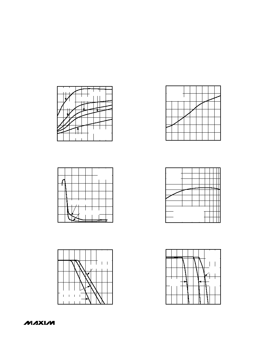
SUPPLY CURRENT
vs. C3 CAPACITOR VALUE
MAX1822 toc01
C3 CAPACITOR VALUE (
µF)
SUPPLY CURRENT (
µ
A)
V
CC
= +5V, I
OUT
= 0
T
A
= +25
°C
C1 = C2 = C*
C* = 0.01
µF
C* = 0.1
µF
C* = 0.033
µF
C* = 0.047
µF
C* =
0.022
µF
50
150
100
200
250
350
300
400
1
4
5
2
3
6
7
8
9
10
MAX1822 toc02
C3 CAPACITOR VALUE (
µF)
SUPPLY CURRENT (
µ
A)
MAX1822
SUPPLY CURRENT
vs. C3 CAPACITOR VALUE
V
CC
= +16.5V
I
OUT
= 0
T
A
= +25
°C
C1 = C2 = 0.01
µF
0
0.2
0.6
0.4
1.0
1.2
0.8
1.4
2
6
8
4
10
12
14
16
18
MAX1822 toc03
V
CC
(V)
SUPPLY CURRENT (mA)
MAX1822
SUPPLY CURRENT
vs. SUPPLY VOLTAGE
C1 = C2 = 0.01
µF
I
OUT
= 0
C3 = 1
µF
T
A
= +25
°C
C1 = C2 = 0.47
µF
12
13
14
15
16
17
0
0.8 1.0
0.4 0.6
0.2
1.2 1.4 1.6 1.8 2.0
MAX1822 toc05
I
OUT
(mA)
V
OUT
(V)
MAX1822
OUTPUT VOLTAGE
vs. OUTPUT CURRENT
C1 = C2 = 0.01
µF
V
CC
= +5V
C3 = 10
µF
T
A
= +25
°C
C1 = C2 = 0.22
µF
C1 = C2 = 0.47
µF
0
200
100
400
300
600
500
700
900
800
1000
0.01
0.1
MAX1822 toc04
C1 = C2 CAPACITANCE VALUE (
µF)
MAXIMUM I
OUT
(
µ
A)
MAX1822
MAXIMUM OUTPUT CURRENT
vs. C1 = C2 CAPACITOR VALUE
V
CC
= +5V
C3 = 10
µF
T
A
= +25
°C
NOTE: MAXIMUM I
OUT
IS THE LOAD
CURRENT AT THE POINT
WHERE V
OUT
BEGINS TO
LOSE REGULATION.
18
21
20
19
22
23
24
0
4
3
1
2
5
6
7
8
9
10
MAX1822 toc05
I
OUT
(mA)
V
OUT
(V)
MAX1822
OUTPUT VOLTAGE
vs. OUTPUT CURRENT
C1 = C2
0.047
µF
C1 = C2
0.022
µF
C1 = C2
0.01
µF
V
CC
= +12V
C3 = 10
µF
T
A
= +25
°C
__________________________________________Typical Operating Characteristics
MAX1822
High-Side Power Supply
4
_______________________________________________________________________________________
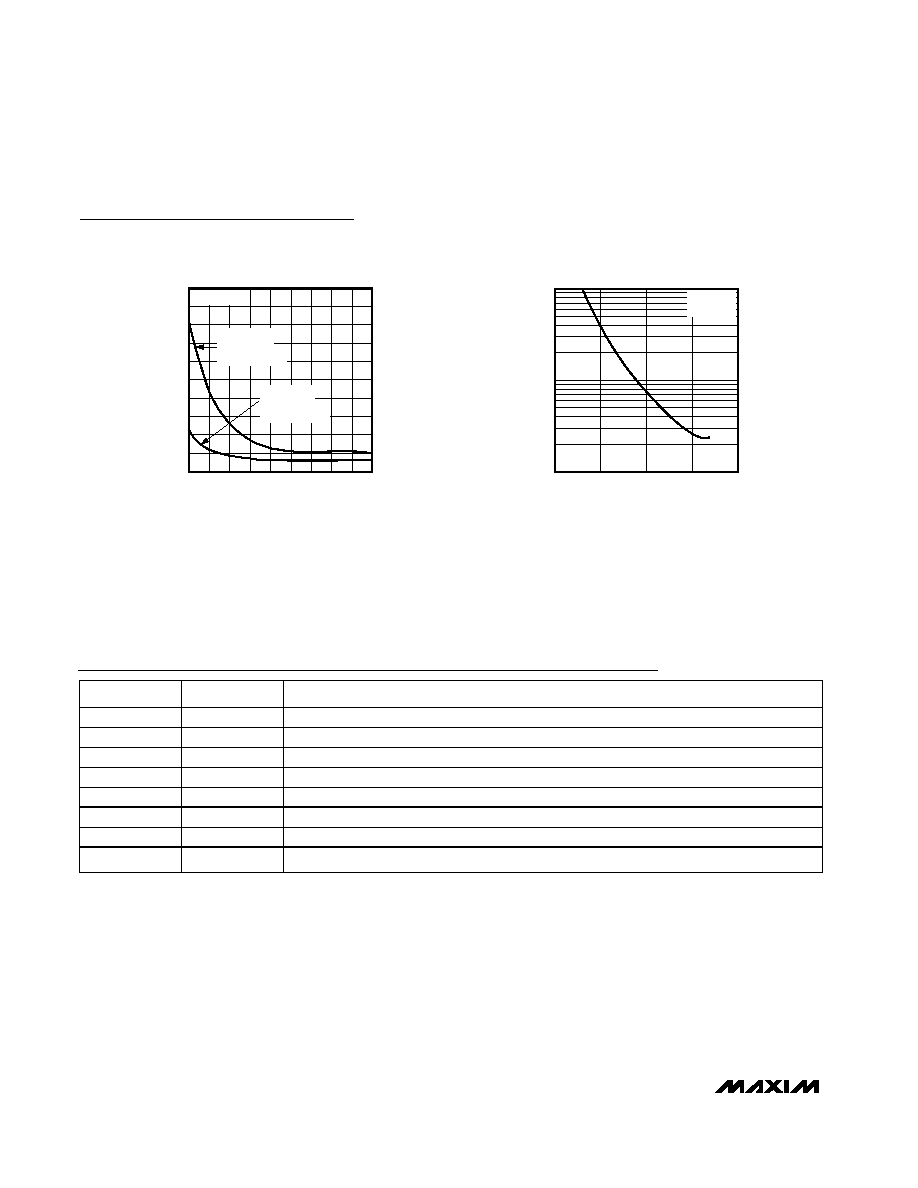
Pin Description
0
40
20
80
60
120
100
140
180
160
200
1
3
4
5
2
6
7
8
9
10
MAX1822 toc07
RESERVOIR CAPACITOR (
µF)
V
OUT
RIPPLE (mV)
MAX1822
OUTPUT VOLTAGE RIPPLE
vs. RESERVOIR CAPACITOR C3
T
A
= +25
°C
V
CC
= +5V
I
OUT
= 500
µA
C1 = C2 = 0.047
µF
V
CC
= +16.5V
I
OUT
= 1mA
C1 = C2 = 0.01
µF
0
5
10
15
20
MAX1822 toc08
V
CC
(V)
0.1
1
10
TURN-ON TIME (ms)
MAX1822
TURN-ON TIME
vs. SUPPLY VOLTAGE
I
OUT
= 0
T
A
= +25
°C
Typical Operating Characteristics (continued)
PIN
NAME
FUNCTION
1
C1+
Positive terminal to primary charge-pump capacitor
2
C2-
Negative terminal to secondary charge-pump capacitor
3
PR
Power-Ready Output. High when V
OUT
is
V
CC
+ 8.5V with respect to GND.
4
GND
Ground
5
V
OUT
High-Side Voltage Out
6
C2+
Positive terminal to secondary charge-pump capacitor
7
C1-
Negative terminal to primary charge-pump capacitor
8
V
CC
Input Supply
MAX1822
High-Side Power Supply
_______________________________________________________________________________________
5
Detailed Description
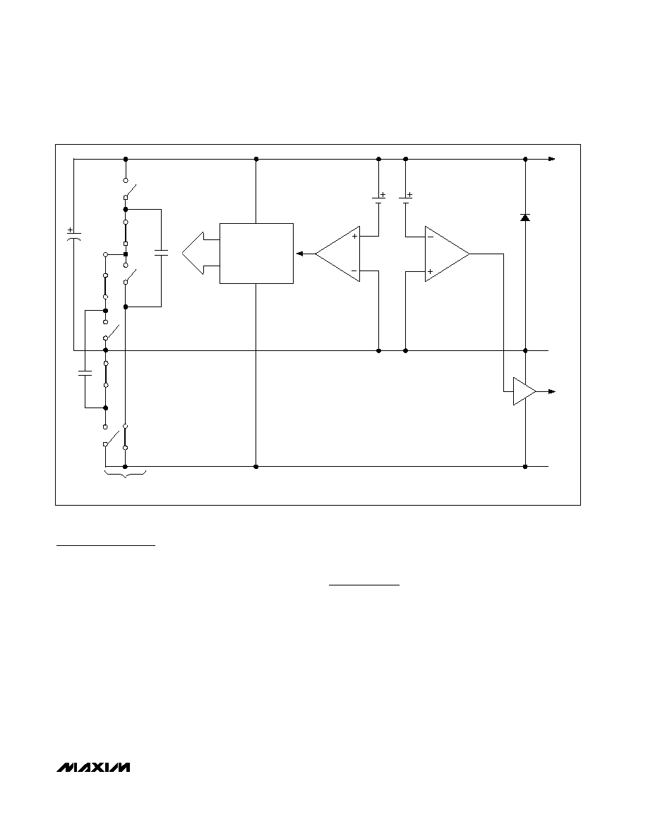
Charge-Pump Operation
The MAX1822 is a multistage charge-pump power sup-
ply. Although the charge pump is capable of multiply-
ing V
CC
up to four times, the output is regulated to V
CC
+ 11V by an internal feedback circuit for inputs above
4V. The charge pump typically operates at 90kHz, but
regulates by pulse skipping. When V
OUT
exceeds V
CC
+ 11V, the oscillator shuts off. As V
OUT
dips below V
CC
+ 11V, the oscillator turns on.
Power-Ready Output
The Power-Ready Output (PR) signals control circuitry
when the high-side voltage reaches a preset level. This
feature can be used to protect external FET switches
from excess dissipation and damage by preventing them
from turning on, except when adequate gate drive levels
are present. When power is applied, PR remains low until
V
OUT
reaches approximately V
CC
+ 8.5V. PR also goes
low if V
OUT
falls below this level during operation, i.e., if
the output is overloaded. The PR high level is V
CC
.
Applications Information
Quiescent Supply Current
MAX1822 quiescent supply current varies with V
CC
and
with the values of C1, C2, and C3 (Typical Operating
Characteristics). Even with no external load, the device
must still pump to overcome internal losses. Large ratios
between C3 and C1 or C2 require more charge-pump
cycles to restore V
OUT
. As V
CC
falls below 5V, quiescent
current rises fairly rapidly to about 1mA at 4V (Typical
Operating Characteristics). This rise occurs because
V
OUT
no longer pulse skips to regulate at low input volt-
ages; the oscillator runs continuously, so supply current
is higher. Figure 2 shows the test circuit for the
MAX1822 quiescent supply current.
Figure 1. MAX1822 Block Diagram
C3
C1
S2
S1
TWO-STAGE CHARGE PUMP
(SWITCHES SHOWN IN REFRESH MODE)
S5
RC OSCILLATOR
+
CONTROL LOGIC
OVERVOLTAGE
COMPARATOR
POWER-READY
COMPARATOR
PR DRIVER
GND
PR
V
CC
11V
8.5V
V
OUT
C2
S6
S7
V
INT
S8
S3
S4