
General Description
The MAX1775 is a dual, step-down DC-DC converter
that generates both the main (+3.3V at over 2A) and
core (+1.8V at up to 1.5A) supplies for a complete
power solution for PDAs, subnotebooks, and other
hand-held devices. The main output is adjustable from
+1.25V to +5.5V. The core output is adjustable from 1V
to 5V. Both switching converters operate at up to
1.25MHz for small external components and use syn-
chronous rectifiers to achieve efficiencies up to 95%.
Operation with up to 100% duty cycle provides the low-
est possible dropout voltage to extend useful battery
life.
The MAX1775 accepts inputs from +2.7V up to +28V,
allowing use with many popular battery configurations as
well as AC-DC wall adapters. Digital soft-start reduces
battery current surges at power-up. Both the main and
core converters have separate shutdown inputs. The
MAX1775 comes in a small 16-pin QSOP package.
The MAX1775 evaluation kit is available to help reduce
design time.
________________________Applications
Hand-Held Computers
PDAs
Internet Access Tablets
POS Terminals
Subnotebooks
Features
o Dual, High-Efficiency, Synchronous Rectified
Step-Down Converter
o Main Power
Adjustable from +1.25V to +5.5V
Over 2A Load Current
Up to 95% Efficiency
o Core Power
Adjustable from 1V to 5V
Internal Switches
Up to 1.5A Load Current
Up to 92% Efficiency
o 100% (max) Duty Cycle
o Up to 1.25MHz Switching Frequency
o Input Voltage Range from +2.7V to +28V
o 170µA Quiescent Current
o 5µA Shutdown Current
o Digital Soft-Start
o Independent Shutdown Inputs
MAX1775
Dual-Output Step-Down
DC-DC Converter for PDA/Palmtop Computers
________________________________________________________________ Maxim Integrated Products
1
16
15
14
13
12
11
10
9
1
2
3
4
5
6
7
8
SHDNM
LXC
INC
GND
FBC
CS-
CS+
FBM
REF
TOP VIEW
MAX1775
16 QSOP
SHDNC
PGND
IN
NDRV
CVL
PDRV
CVH
Pin Configuration
19-1811; Rev 1; 8/01
EVALUA
TION KIT
AVAILA
BLE
Ordering Information
PART
TEMP. RANGE
PIN-PACKAGE
MAX1775EEE
-40
°C to +85°C
16 QSOP
SHDNM
IN
IN 2.7V TO 5.5V (28V IN CASCADE)
CVH
CORE
1.8V
1.5A
MAIN
3.3V
OVER 2A
SHDNC
ON
ON
OFF
OFF
NDRV
CS+
CS-
INC
FBM
LXC
FBC
CVL
REF
PGND
GND
PDRV
MAX1775
Typical Operating Circuit
For pricing, delivery, and ordering information, please contact Maxim/Dallas Direct! at
1-888-629-4642, or visit Maxim's website at www.maxim-ic.com.
MAX1775
Dual-Output Step-Down
DC-DC Converter for PDA/Palmtop Computers
2
_______________________________________________________________________________________
ABSOLUTE MAXIMUM RATINGS
ELECTRICAL CHARACTERISTICS
(V
IN
= +12V, V
MAIN
= V
INC
= V
CS-
= V
CS+
= +3.3V, V
CORE
= +1.8V, Circuit of Figure 4, T
A
= 0°C to +85°C, unless otherwise noted.
Typical values are at T
A
= +25°C.)
Stresses beyond those listed under "Absolute Maximum Ratings" may cause permanent damage to the device. These are stress ratings only, and functional
operation of the device at these or any other conditions beyond those indicated in the operational sections of the specifications is not implied. Exposure to
absolute maximum rating conditions for extended periods may affect device reliability.
IN, SHDNM, CVH to GND.......................................-0.3V to +30V
IN to CVH, PDRV ......................................................-0.3V to +6V
PDRV to GND..................................(V
CVH
- 0.3V) to (V
IN
+ 0.3V)
PGND to GND .......................................................-0.3V to +0.3V
All Other Pins to GND...............................................-0.3V to +6V
Core Output Short Circuit...........................................Continuous
Continuous Power Dissipation
16-Pin QSOP (derate 7.1mW/°C above +70°C)..........571mW
Operating Temperature .......................................-40°C to +85°C
Storage Temperature.........................................-65°C to +150°C
Lead Temperature (soldering, 10s) .................................+300°C
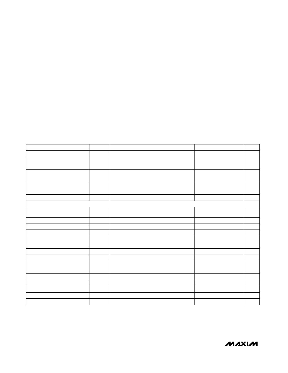
PARAMETER
SYMBOL
CONDITIONS
MIN
TYP
MAX
UNITS
Input Voltage
V
IN
2.7
28
V
Input Quiescent Supply Current
I
IN
V
FBM
= +1.5V, V
FBC
= +1.5V,
V
SHDNM
= V
SHDNC
= +3.3V
15
30
µA
CS- Quiescent Supply Current
I
CS
-
V
FBM
= +1.5V, V
FBC
= +1.5V,
V
SHDNM
= V
SHDNC
= +3.3V
110
220
µA
Core Regulator Quiescent
Supply Current
I
INC
V
FBM
= +1.5V, V
FBC
= +1.5V,
V
SHDNM
= V
SHDNC
= +3.3V
60
120
µA
IN Shutdown Supply Current
SHDNM = SHDNC = GND
5
30
µA
MAIN REGULATOR
Main Output Voltage Adjust
Range
1.25
5.5
V
FBM Regulation Threshold
V
FBM
V
( C S + - C S - )
= 0 to + 60m V , V
IN
= + 2.7V to + 28V 1.21
1.25
1.29
V
FBM Input Current
I
FBM
V
FBM
= +1.3V
-0.1
0.1
µA
Current-Limit Threshold
V
CLM
V
CS+
- V
CS-
60
80
100
mV
Minimum Current-Limit
Threshold
V
MIN
V
CS+
- V
CS
-
6
15
24
mV
Valley Current Threshold
V
VALLEY
V
CS+
- V
CS
-
40
50
60
mV
Zero Current Threshold
V
ZERO
V
CS+
- V
CS
-
0
15
mV
PDRV, NDRV Gate Drive
Resistance
V
CS
- = +3.3V, I
LOAD
= 50mA
2
4.4
CS- to CVL Switch Resistance
I
CVL
= 50mA
4.5
8
PDRV, NDRV Dead Time
50
ns
Maximum Duty Cycle
100
%
Minimum On-Time
200
400
650
ns
Minimum Off-Time
200
400
650
ns

MAX1775
Dual-Output Step-Down
DC-DC Converter for PDA/Palmtop Computers
_______________________________________________________________________________________
3
ELECTRICAL CHARACTERISTICS (continued)
(V
IN
= +12V, V
MAIN
= V
INC
= V
CS-
= V
CS+
= +3.3V, V
CORE
= +1.8V, Circuit of Figure 4, T
A
= 0°C to +85°C, unless otherwise noted.
Typical values are at T
A
= +25°C.)
PARAMETER
SYMBOL
CONDITIONS
MIN
TYP
MAX
UNITS
CORE REGULATOR
Input Voltage Range
V
INC
2.6
5.5
V
V
INC
rising
2.40
2.47
2.55
INC Undervoltage Lockout
V
INC
falling
2.30
2.37
2.45
V
Core Output Voltage Adjust
Range
1.0
5.0
V
Maximum Core Load Current
(Note 1)
1
1.5
A
FBC Regulation Threshold
V
FBC
V
INC
= +2.5 to +5.5V, I
OUTC
= 0 to 200mA
0.97
1.0
1.03
V
FBC Input Current
I
FBC
V
FBC
= +1.3V
-0.1
0.1
µA
Dropout Voltage (INC to LXC)
I
OUTC
= 400mA
0.1
0.25
V
LXC Leakage Current
I
LXC
V
INC
= +5.5V, V
LXC
= 0 to +5.5V
-10
10
µA
LXC P-Channel, N-Channel
On-Resistance
0.25
0.5
LXC P-Channel Current Limit
I
CLC
1200
1800
3000
mA
LXC P-Channel Minimum
Current
100
200
400
mA
LXC N-Channel Valley Current
900
1400
2400
mA
LXC N-Channel Zero-Crossing
Current
40
110
170
mA
LXC Dead Time
50
ns
Maximum Duty Cycle
100
%
Minimum On-Time
170
400
670
ns
Minimum Off-Time
170
400
670
ns
REFERENCE
Reference Voltage
V
REF
1.23
1.25
1.27
V
Reference Load Regulation
I
REF
= 0 to 50µA
10
mV
Reference Line Regulation
V
CS
- = +2.5V to +5.5V, I
REF
= 50µA
5
mV
Reference Sink Current
I
REF
10
µA
CVL, CVH REGULATORS
I
CVL
= 50mA, V
IN
= +2.7V, V
CS
- = 0
2.6
2.8
3.1
CVL Output Voltage
V
CVL
I
CVL
= 50mA, V
CS
- = +3.3V
3.2
V
CVL Switchover Threshold
V
CS-
rising, hysteresis = 100mV (typ)
2.40
2.47
2.55
V
V
IN
= +4V, I
CVH
= 25mA
V
IN
- 3.4 V
IN
- 2.8
CVH Output Voltage
V
CVH
V
IN
= +12V, I
CVH
= 50mA
V
IN
- 4.3 V
IN
- 3.7
V
CVH Switchover Threshold
V
IN
V
IN
rising, hysteresis = 350mV (typ)
5.5
V
V
CVL
rising
2.40
2.47
2.55
CVL Undervoltage Lockout
V
CVL
falling
2.30
2.37
2.45
V

MAX1775
Dual-Output Step-Down
DC-DC Converter for PDA/Palmtop Computers
4
_______________________________________________________________________________________
PARAMETER
SYMBOL
CONDITIONS
MIN
TYP
MAX
UNITS
LOGIC INPUTS
SHDNM, SHDNC Input Low
Voltage
0.4
V
SHDNM, SHDNC Input High
Voltage
2.0
V
SHDNM, SHDNC Input Low
Current
SHDNM = SHDNC = GND
-1
1
µA
SHDNC Input High Current
V
SHDNC
= +5.5V
5
µA
V
SHDNM
= +5V
2
SHDNM Input High Current
V
SHDNM
= +28V
15
30
µA
ELECTRICAL CHARACTERISTICS (continued)
(V
IN
= +12V, V
MAIN
= V
INC
= V
CS-
= V
CS+
= +3.3V, V
CORE
= +1.8V, Circuit of Figure 4, T
A
= 0°C to +85°C, unless otherwise noted.
Typical values are at T
A
= +25°C.)
ELECTRICAL CHARACTERISTICS
(V
IN
= +12V, V
MAIN
= V
INC
= V
CS-
= V
CS+
= +3.3V, V
CORE
= +1.8V, Circuit of Figure 4, T
A
-40°C to +85°C, unless otherwise noted.)
(Note 2)
PARAMETER
SYMBOL
CONDITIONS
MIN
MAX
UNITS
Input Voltage
V
IN
2.7
28
V
Input Quiescent Supply Current
I
IN
V
FBM
= +1.5V, V
FBC
= +1.5V,
V
SHDNM
= V
SHDNC
= +3.3V
30
µA
CS- Quiescent Supply Current
I
CS-
V
FBM
= +1.5V, V
FBC
= +1.5V,
V
SHDNM
= V
SHDNC
= +3.3V
220
µA
Core Regulator Quiescent
Supply Current
I
INC
V
FBM
= +1.5V, V
FBC
= +1.5V,
V
SHDNM
= V
SHDNC
= +3.3V
120
µA
IN Shutdown Supply Current
SHDNM = SHDNC = GND
30
µA
MAIN REGULATOR
Main Output Voltage Adjust
Range
1.25
5.5
V
FBM Regulation Threshold
V
FBM
V
( C S + - C S - )
= 0 to + 60m V , V
I N
= + 2.7V to + 28V 1.21
1.29
V
FBM Input Current
I
FBM
V
FBM
= +1.3V
-0.1
0.1
µA
Current-Limit Threshold
V
CL
V
CS+
- V
CS-
60
100
mV
M i ni m um C ur r ent- Li m i t Thr eshol d V
CS+
- V
CS-
6
24
mV
Valley Current Threshold
V
CS+
- V
CS-
40
60
mV
Zero Current Threshold
V
CS+
- V
CS-
0
15
mV
PDRV, NDRV Gate Drive
Resistance
V
CS-
= +3.3V
4.4
CS- to CVL Switch Resistance
I
CVL
= 50mA
8

MAX1775
Dual-Output Step-Down
DC-DC Converter for PDA/Palmtop Computers
_______________________________________________________________________________________
5
ELECTRICAL CHARACTERISTICS (continued)
(V
IN
= +12V, V
MAIN
= V
INC
= V
CS-
= V
CS+
= +3.3V, V
CORE
= +1.8V, Circuit of Figure 4, T
A
-40°C to +85°C, unless otherwise noted.)
(Note 2)
PARAMETER
SYMBOL
CONDITIONS
MIN
MAX
UNITS
Maximum Duty Cycle
100
%
Minimum On-Time
200
650
ns
Minimum Off-Time
200
650
ns
CORE REGULATOR
Input Voltage Range
V
INC
2.6
5.5
V
V
INC
rising
2.39
2.55
INC Undervoltage Lockout
V
INC
falling
2.29
2.45
V
Core Output Voltage Adjust
Range
1.0
5.0
V
Maximum Core Load Current
(Note 1)
1
A
FBC Regulation Threshold
V
FBC
V
INC
= +2.5V to +5.5V, I
OUTC
= 0 to 200mA
0.97
1.03
V
FBC Input Current
I
FBC
V
FBC
= +1.3V
-0.1
0.1
µA
Dropout Voltage (INC to LXC)
I
OUTC
= 400mA
0.2
V
LXC Leakage Current
I
LXC
V
INC
= +5.5V, V
LXC
= 0 to +5.5V
-10
10
µA
LXC P-Channel, N-Channel
On-Resistance
0.5
LXC P-Channel Current Limit
1200
3050
mA
LXC P-Channel Minimum
Current
100
400
mA
LXC N-Channel Valley Current
880
2450
mA
LXC N-Channel Zero-Crossing
Current
35
175
mA
Maximum Duty Cycle
100
%
Minimum On-Time
150
670
ns
Minimum Off-Time
150
670
ns
REFERENCE
Reference Voltage
V
REF
1.22
1.27
V
Reference Load Regulation
I
REF
= 0 to 50µA
10
mV
Reference Line Regulation
V
CS-
= +2.5V to +5.5V,
I
REF
= 50µA
5
mV
Reference Sink Current
I
REF
10
µA
CVL, CVH REGULATORS
CVL Output Voltage
V
CVL
I
CVL
= 50mA, V
IN
= +2.7V, V
CS-
= 0
2.6
3.1
V
V
IN
= +4V, I
CVH
= 25mA
V
IN
- 2.8
CVH Output Voltage
V
CVH
V
IN
= +12V, I
CVH
= 50mA
V
IN
- 3.7
V
V
CVL
rising
2.40
2.55
CVL Undervoltage Lockout
V
CVL
falling
2.30
2.45
V