Äîêóìåíòàöèÿ è îïèñàíèÿ www.docs.chipfind.ru
General Description
The MAX1761 dual pulse-width-modulation (PWM),
step-down controller provides high efficiency, excellent
transient response, and high DC output accuracy in an
extremely compact circuit topology. These features are
essential for stepping down high-voltage batteries to
generate low-voltage CPU core, I/O, and chipset RAM
supplies in PC board area critical applications, such as
notebook computers and smart phones.
Maxim's proprietary Quick-PWMTM quick-response,
constant-on-time PWM control scheme handles wide
input/output voltage ratios with ease and provides
"instant-on" response to load transients while maintain-
ing a relatively constant switching frequency.
The MAX1761 achieves high efficiency at reduced cost
by eliminating the current-sense resistor found in tradi-
tional current-mode PWMs. Efficiency is further
enhanced by its ability to drive large synchronous-recti-
fier MOSFETs. The MAX1761 employs a complemen-
tary MOSFET output stage, which reduces component
count by eliminating external bootstrap capacitors and
diodes.
Single-stage buck conversion allows this device to
directly step down high-voltage batteries for the highest
possible efficiency. Alternatively, two-stage conversion
(stepping down the +5V system supply instead of the
battery) at a higher switching frequency allows the mini-
mum possible physical size.
The MAX1761 is intended for CPU core, chipset,
DRAM, or other low-voltage supplies. The MAX1761 is
available in a 16-pin QSOP package. For applications
requiring greater output power, refer to the MAX1715
data sheet. For a single-output version, refer to the
MAX1762/MAX1791 data sheet.
________________________Applications
Notebooks and PDAs
Digital Cameras
Handy-Terminals
Smart Phones
1.8V/2.5V Logic and I/O Supplies
Features
o Free-Running On-Demand PWM
o Selectable Light-Load Pulse-Skipping Operation
o ±1% Total DC Error in Forced-PWM Mode
o 5V to 20V Input Range
o Flexible Output Voltages
OUT1: Dual ModeTM Fixed 2.5V or 1V to 5.5V
Adjustable
OUT2: Dual Mode Fixed 1.8V or 1V to 5.5V
Adjustable
o Output Undervoltage Protection
o Complementary Synchronous Buck
o No Current-Sense Resistor
o 4.65V at 25mA Linear Regulator Output
o 4µA V+ Shutdown Supply Current
o 5µA VL Shutdown Supply Current
o 950µA Quiescent Supply Current
o Tiny 16-Pin QSOP Package
MAX1761
Small, Dual, High-Efficiency
Buck Controller for Notebooks
________________________________________________________________ Maxim Integrated Products
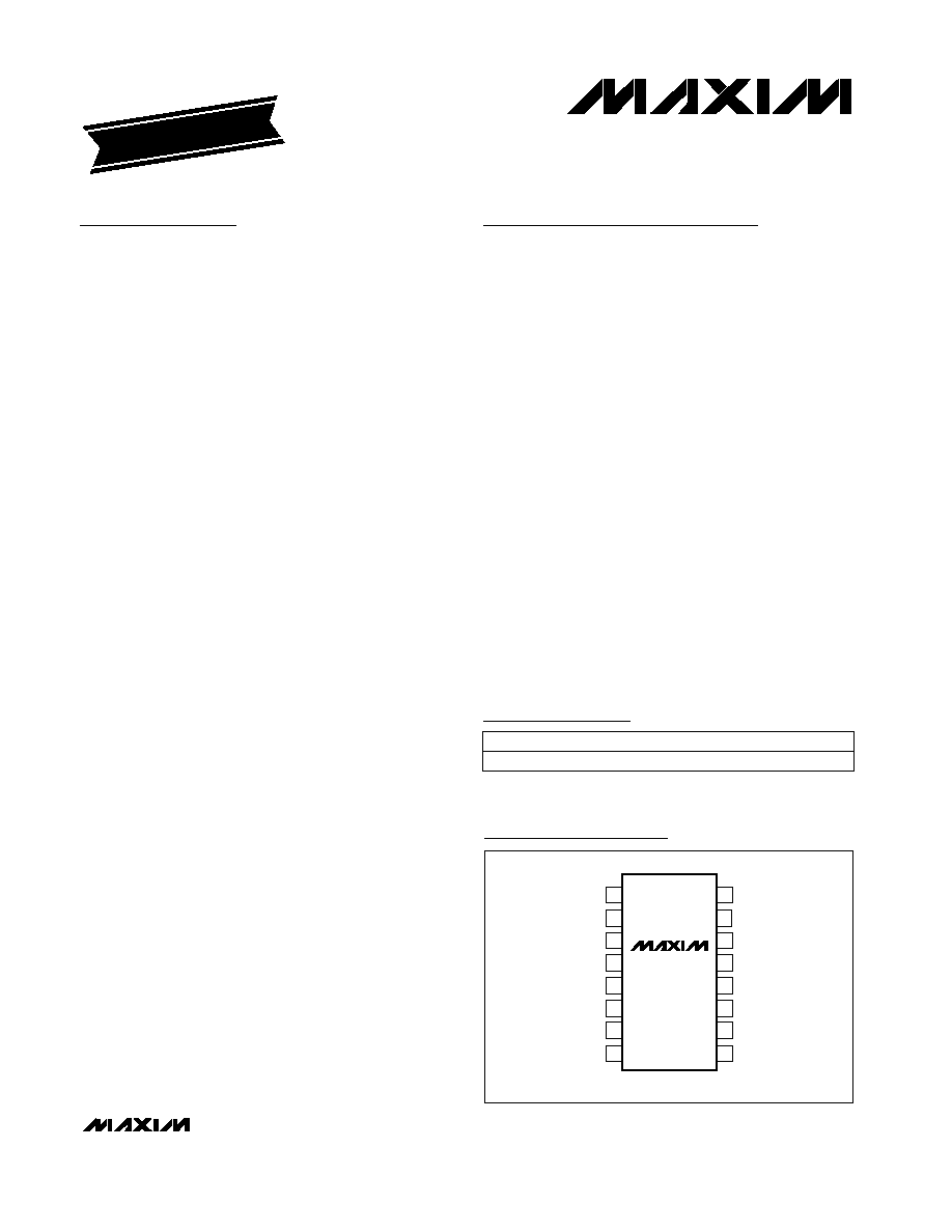
1
16
15
14
13
12
11
10
9
1
2
3
4
5
6
7
8
FB1
DH1
CS1
DL1
VL
GND
DL2
CS2
DH2
TOP VIEW
MAX1761
QSOP
OUT1
REF
ON1
ON2
V+
OUT2
FB2
Pin Configuration
19-1835; Rev 0; 10/00
For price, delivery, and to place orders, please contact Maxim Distribution at 1-888-629-4642,
or visit Maxim's website at www.maxim-ic.com.
EVALUATION KIT
AVAILABLE
Ordering Information
16 QSOP
PIN-PACKAGE
TEMP. RANGE
-40°C to +85°C
MAX1761EEE
PART
Quick-PWM and Dual Mode are trademarks of
Maxim Integrated Products.
MAX1761
Small, Dual, High-Efficiency
Buck Controller for Notebooks
2
_______________________________________________________________________________________
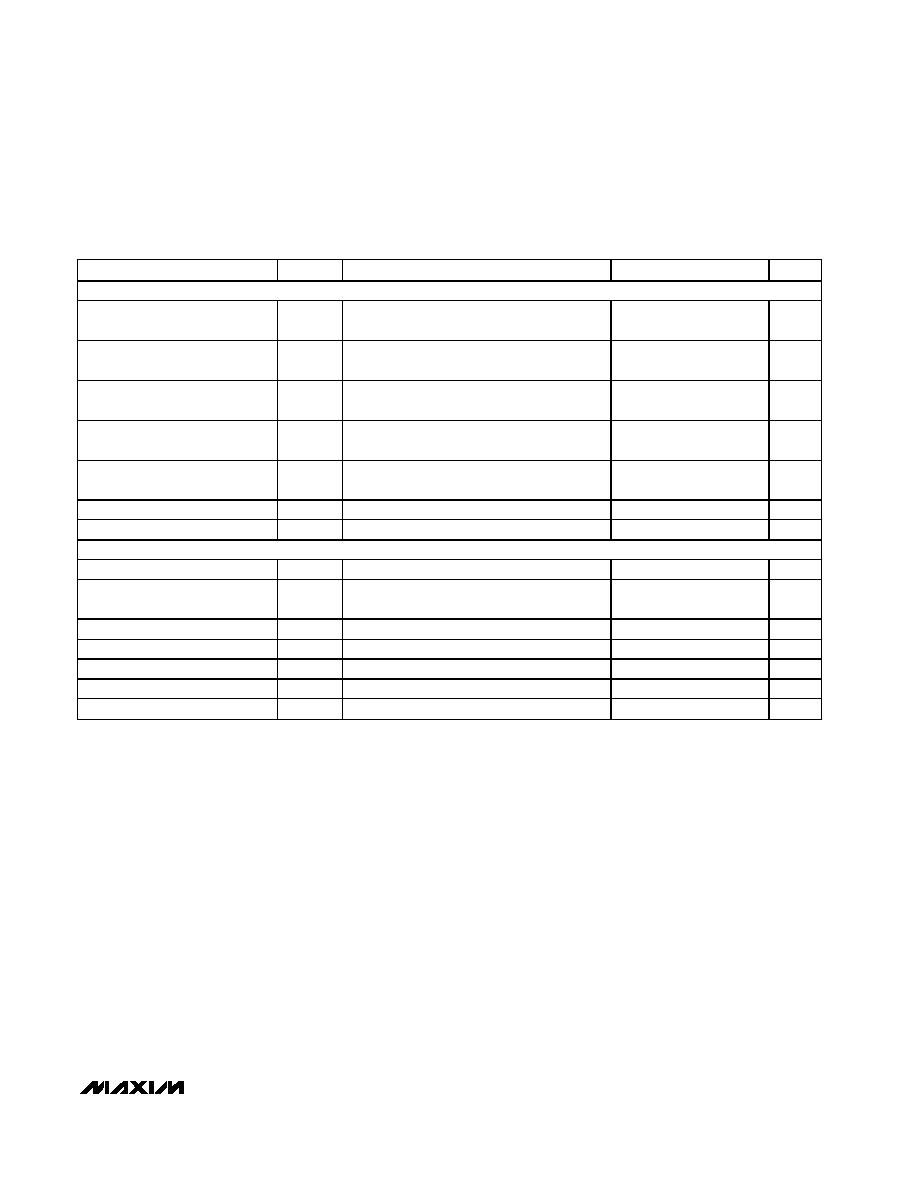
ABSOLUTE MAXIMUM RATINGS
ELECTRICAL CHARACTERISTICS
(Circuit of Figure 1, V+ = 15V, C
VL
= 4.7µF, C
REF
= 0.1µF, VL not externally driven unless otherwise noted, T
A
= 0°C to +85°C, unless
otherwise noted.) (Note 1)
Stresses beyond those listed under "Absolute Maximum Ratings" may cause permanent damage to the device. These are stress ratings only, and functional
operation of the device at these or any other conditions beyond those indicated in the operational sections of the specifications is not implied. Exposure to
absolute maximum rating conditions for extended periods may affect device reliability.
V+ to GND ..............................................................-0.3V to +22V
VL to GND ................................................................-0.3V to +6V
VL to V+ .............................................................................+0.3V
OUT_, ON2 to GND ..................................................-0.3V to +6V
ON1, DH_ to GND ........................................-0.3V to (V+ + 0.3V)
FB_, REF, DL_ to GND.................................-0.3V to (VL + 0.3V)
CS_ to GND .....................................................-2V to (V+ + 0.3V)
REF Short Circuit to GND ...........................................Continuous
Continuous Power Dissipation
16-Pin QSOP (derate 8.3mW/°C above +70°C) ..........667mW
Operating Temperature Range ...........................-40°C to +85°C
Junction Temperature ......................................................+150°C
Storage Temperature.........................................-65°C to +150°C
Lead Temperature (soldering, 10s) .................................+300°C
PARAMETER
SYMBOL
CONDITIONS
MIN
TYP
MAX
UNITS
PWM CONTROLLERS
Input Voltage Range
V+
(Note 2)
4.5
20
V
FB_ = OUT_
0.99
1
1.01
FB1 = GND
2.475
2.5
2.525
V
DC Output Voltage Accuracy
(Note 3)
V
OUT_
V+
= 4.5V to 20V,
VL
= 4.75V to 5.25V,
ON2 = VL
FB2 = GND
1.782
1.8
1.818
Output Voltage Adjust Range
1
5.5
V
OUT_ Input Resistance
80
160
300
k
FB_ Input Bias Current
V
FB_
= 1V, VL = 5V
-0.1
0.1
µA
CS_ Input Bias Current
V
CS_
= 0, VL = 5V
-1
1
µA
Soft-Start Ramp Time
Zero to full ILIM
1700
µs
OUT1
661
735
809
On-Time (Note 4)
t
ON
V+
= 10V, V
OUT1
= 2.5V,
V
OUT2
= 1.8V
OUT2
648
720
792
ns
Minimum Off-Time (Note 4)
t
OFF
400
500
ns
BIAS AND REFERENCE
IL
FB1 = FB2 = GND, VL = 5V, V
OUT1
and
V
OUT2
forced above regulation point
0.60
1.20
mA
VL undriven
0.95
1.70
Quiescent Supply Current
I+
FB1 = FB2 = GND, V
OUT1
and V
OUT2
forced
above regulation point
VL = 5V
0.38
0.65
mA
IL
VL = 5V, ON1 = ON2 = GND
5
10
µA
Shutdown Supply Current
I+
VL = 0, 5V
4
10
µA
VL Output Voltage
VL
I
LOAD
= 0 to 25mA, V+ = 5V to 20V
4.5
4.65
4.75
V
Reference Voltage
V
REF
V+ = 5V to 20V, no load
1.98
2
2.02
V
Reference Load Regulation
I
REF
I
REF
= 0 to 50µA
8
mV
REF Sink Current
REF in regulation
10
µA
Falling edge
1.6
REF Fault Lockout Voltage
Rising edge
1.94
V
MAX1761
Small, Dual, High-Efficiency
Buck Controller for Notebooks
_______________________________________________________________________________________
3
PARAMETER
SYMBOL
CONDITIONS
MIN
TYP
MAX
UNITS
FAULT PROTECTION
Output Undervoltage Threshold
(Foldback)
V
FB,UVFB
With respect to the regulation point, no load
60
70
80
%
Output Undervoltage Blanking
Time
V
FB,UVLO(t)
Measured from ON_ signal going high
10
32
ms
GND - CS_, positive direction
92
100
108
GND - CS_, negative direction, ON2 = floating
-135
-120
-105
Current-Limit Threshold
GND - CS_, zero crossing, ON2 = 5V
2.5
mV
Thermal Shutdown Threshold
Hysteresis = 10
o
C
160
o
C
VL Undervoltage Lockout
Threshold
V
VL,UVLO
Rising edge, hysteresis = 20mV, PWM is
disabled below this voltage
4.1
4.4
V
GATE DRIVERS
DH_ Gate Driver On-Resistance
(Pullup)
V+ = 6V to 20V, DH_, high state
3.7
8
DH_ Gate Driver On-Resistance
(Pulldown)
DH_, low state
6.2
10
DL_ Gate Driver On-Resistance
(Pullup)
DL_ , high state
3.4
8
DL_ Gate Driver On-Resistance
(Pulldown)
DL_, low state
2.0
5
DH_ Gate Driver Source/Sink
Current
V
DH_
= 3V, V+ = 6V
0.6
A
DL_ Gate Drive Sink Current
V
DL_
= 2.5V
0.9
A
DL_ Gate Drive Source Current
V
DL_
= 2.5V
0.5
A
LOGIC CONTROLS
ON_ Logic Input High Voltage
2.05
V
ON2 Logic Input Float Voltage
(Forced-PWM Mode)
2.0V < V
ON1
< VL
1.3
1.7
1.95
V
ON_ Logic Input Low Voltage
0.5
V
ON1 Logic Input Current
-1
1
µA
ON2 Logic High Input Current
V
ON2
> 2.0V
0
1
3
µA
ON2 Logic Low Input Current
V
ON2
< 0.5V, V
ON1
> 2.0V
-2
-1
0
µA
FB_ Dual Mode Threshold
50
100
150
mV
ELECTRICAL CHARACTERISTICS (continued)
(Circuit of Figure 1, V+ = 15V, C
VL
= 4.7µF, C
REF
= 0.1µF, VL not externally driven unless otherwise noted, T
A
= 0°C to +85°C, unless
otherwise noted.) (Note 1)
MAX1761
Small, Dual, High-Efficiency
Buck Controller for Notebooks
4
_______________________________________________________________________________________
PARAMETER
SYMBOL
CONDITIONS
MIN
TYP
MAX
UNITS
PWM CONTROLLERS
V+
(Note 2)
4.5
20
V
Input Voltage Range
VL
VL externally driven (Note 2)
4.75
5.25
FB_ = OUT_
0.99
1.01
FB1 = GND
2.475
2.525
V
DC Output Voltage Accuracy
(Note 3)
V
OUT_
V+
= 4.5V to 20V,
VL
= 4.75V to 5.25V,
ON2 = VL
FB2 = GND
1.782
1.818
Output Voltage Adjust Range
1
5.5
V
OUT_ Input Resistance
80
300
k
FB_ Input Bias Current
V
FB_
= 1V, VL = 5V
-0.1
0.1
µA
CS_ Input Bias Current
V
CS_
= 0, VL = 5V
-1
1
µA
Soft-Start Ramp Time
Zero to full ILIM
µs
OUT1
661
809
On-Time (Note 4)
t
ON
V+
= 10V, V
OUT1
= 2.5V,
V
OUT2
= 1.8V
OUT2
648
792
ns
Minimum Off-Time (Note 4)
t
OFF
Above regulation point
500
ns
BIAS AND REFERENCE
IL
FB1 = FB2 = GND, VL = 5V, V
OUT1
and
V
OUT2
forced above regulation point
1.2
mA
VL undriven
1.7
Quiescent Supply Current
I+
FB1 = FB2 = GND, V
OUT1
and V
OUT2
forced above
regulation point
VL = 5V
0.5
mA
IL
VL = 5V, ON1 = ON2 = GND
10
µA
Shutdown Supply Current
I+
VL = 0, 5V
10
µA
VL Output Voltage
VL
I
LOAD
= 0 to 25mA, V+ = 5V to 20V
4.5
4.75
V
Reference Voltage
V
REF
V+ = 5V to 20V, no load
1.98
2.02
V
Reference Load Regulation
I
REF
I
REF
= 0 to 50µA
8
mV
REF Sink Current
REF in regulation
10
µA
FAULT PROTECTION
Output Undervoltage Threshold
(Foldback)
V
FB,UVFB
With respect to the regulation point, no load
60
80
%
Output Undervoltage Lockout
Timer
V
FB,UVLO(t)
Measured from ON_ signal going high
10
32
ms
GND CS_, positive direction
92
108
Current-Limit Threshold
GND CS_, negative direction, ON2 = floating
-135
-105
mV
VL Undervoltage Lockout
Threshold
V
VL,UVLO
Rising edge, hysteresis = 20mV, PWM is
disabled below this voltage
4.1
4.4
V
ELECTRICAL CHARACTERISTICS
(Circuit of Figure 1, V+ = 15V, C
VL
= 4.7µF, C
REF
= 0.1µF, VL not externally driven unless otherwise noted, T
A
= -40°C to +85°C,
unless otherwise noted.) (Note 1)
MAX1761
Small, Dual, High-Efficiency
Buck Controller for Notebooks
_______________________________________________________________________________________
5
PARAMETER
SYMBOL
CONDITIONS
MIN
TYP
MAX
UNITS
GATE DRIVERS
DH_ Gate Driver On-Resistance
(Pullup)
V+ = 6V to 20V, DH_, high state
8
DH_ Gate Driver On-Resistance
(Pulldown)
DH_, low state
10
DL_ Gate Driver On-Resistance
(Pullup)
DL_, high state
8
DL_ Gate Driver On-Resistance
(Pulldown)
DL_, low state
5
DH_ Gate Driver Source/Sink
Current
V
DH_
= 3V, V+ = 6V
A
DL_ Gate Drive Sink Current
V
DL_
= 2.5V
A
DL_ Gate Driver Source Current
V
DL_
= 2.5V
A
LOGIC CONTROLS
ON_ Logic Input High Voltage
2.05
V
ON2 Logic Input Float Voltage
(Forced-PWM Mode)
V
ON1
> 2.0V
1.3
1.95
V
ON_ Logic Input Low Voltage
0.5
V
ON1 Logic Input Current
-1
1
µA
ON2 Logic High Input Current
V
ON2
> 2.0V
0
3
µA
ON2 Logic Low Input Current
V
ON2
< 0.5V, V
ON1
> 2.0V
-2
0
µA
FB_ Dual Mode Threshold
50
150
mV
ELECTRICAL CHARACTERISTICS (continued)
(Circuit of Figure 1, V+ = 15V, C
VL
= 4.7µF, C
REF
= 0.1µF, VL not externally driven unless otherwise noted, T
A
= -40°C to +85°C,
unless otherwise noted.) (Note 1)
Note 1: Specifications to -40°C are guaranteed by design, not production tested.
Note 2: If V+ is less than 5V, V+ must be connected to VL. If VL is connected to V+, V+ must be between 4.5V and 5.5V.
Note 3: DC output accuracy specifications refer to the trip-level error of the error amplifier. The output voltage will have a DC regula-
tion higher than the trip level by 50% of the ripple. In PFM mode, the output will rise by approximately 1.5% when transition-
ing from continuous conduction to no load.
Note 4: One-shot times are measured at the DH pin (V+ = 15V, C
DH
= 400pF, 90% point to 90% point). Actual in-circuit times may
be different due to MOSFET switching speeds.This effect can also cause the switching frequency to vary.