General Description
The MAX1749 allows for a constant vibration force while
operating from a +2.5V to +6.5V input range and deliver-
ing up to 120mA. A PMOS pass transistor allows the
80µA supply current to remain independent of the load.
The output voltage can be adjusted from +1.25V to V
IN
with an external resistor-divider. When turned off
(ON = low), the MAX1749 supply current drops to 1µA
(max) to minimize battery drain. Other features include
short-circuit protection, thermal shutdown protection,
and reverse battery protection. The MAX1749 is avail-
able in a 5-pin SOT23 package.
________________________Applications
Wireless Handset Vibrator Motor Drivers
Pager Vibrator Motor Drivers
____________________________Features
o
Fixed 1.25V or Adjustable (1.25V to 6.5V) Output
o
Low Cost
o
Thermal Overload Protection
o
Output Current Limit
o
Reverse Battery Protection
o
Low 0.1nA Off Supply Current
o
Low 80µA Full-Load Supply Current
MAX1749
SOT23 Vibrator Motor Driver
________________________________________________________________
Maxim Integrated Products
1
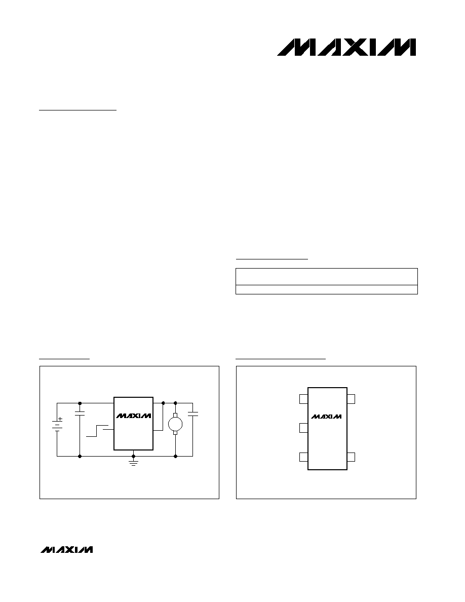
SOT23-5
TOP VIEW
GND
OUT
IN
1
5
SET
ON
MAX1749
2
3
4
Pin Configuration
MAX1749
OUT
GND
IN
ON
SET
C
OUT
1
µ
F
C
IN
1
µ
F
BATTERY
1.25V
UP TO 120mA
2.5V TO 6.5V
ON
OFF
Typical Operating Circuit
19-1455; Rev 1; 6/99
PART
MAX1749EUK-T
-40°C to +85°C
TEMP. RANGE
PIN-
PACKAGE
5 SOT23
Ordering Information
TOP
MARK
ADIX
For free samples & the latest literature: http://www.maxim-ic.com, or phone 1-800-998-8800.
For small orders, phone 1-800-835-8769.

MAX1749
SOT23 Vibrator Motor Driver
2
_______________________________________________________________________________________
ABSOLUTE MAXIMUM RATINGS
ELECTRICAL CHARACTERISTICS
(V
IN
= +3.6V, T
A
= -40°C to +85°C, unless otherwise noted. Typical values are at T
A
= +25°C.) (Note 1)
Stresses beyond those listed under "Absolute Maximum Ratings" may cause permanent damage to the device. These are stress ratings only, and functional
operation of the device at these or any other conditions beyond those indicated in the operational sections of the specifications is not implied. Exposure to
absolute maximum rating conditions for extended periods may affect device reliability.
IN to GND ....................................................................-7V to +7V
Output Short-Circuit Duration ............................................Infinite
SET to GND ..............................................................-0.3V to +7V
ON to GND ..................................................................-7V to +7V
ON to IN....................................................................-7V to +0.3V
OUT to GND ................................................-0.3V to (V
IN
+ 0.3V)
Continuous Power Dissipation (T
A
= +70°C)
SOT23-5 (derate 7.1mW/°C above +70°C) .................571mW
Operating Temperature Range ...........................-40°C to +85°C
Junction Temperature ......................................................+150°C
JA
...............................................................................+140°C/W
Storage Temperature Range .............................-65°C to +150°C
Lead Temperature (soldering, 10sec) .............................+300°C
0.05
0
100
I
ON
ON Input Bias Current
V
0.4
V
IL
ON Input High Threshold
2.0
V
IH
V
2.5
6.5
V
IN
Input Voltage
µA
80
200
I
Q
Ground Pin Current
1.13
1.25
1.37
V
V
OUT
Output Voltage
mA
120
Maximum Output Current
UNITS
MIN
TYP
MAX
SYMBOL
PARAMETER
ON = IN
CONDITIONS
mA
280
I
LIM
Current Limit (Note 2)
0.1mA
I
OUT
50mA, SET = OUT
Note 1:
Limits are 100% production tested at T
A
= +25°C. Limits over the operating temperature range are guaranteed through cor-
relation using Statistical Quality Control (SQC) methods.
Note 2:
Not tested. For design purposes, the current limit should be considered 120mA minimum to 420mA maximum.
T
A
= +85°C
T
A
= +25°C
nA
ON Input Low Threshold
V
0.5
T
A
= +85°C
T
A
= +25°C
nA
0.03
10
I
SET
SET Input Leakage Current
V
SET
= 1.4V
°C
170
T
SHDN
Thermal Shutdown Temperature
°C
20
T
SHDN
Thermal Shutdown Hysteresis
µA
0.0001
1
I
OFF
Off Supply Current
V
OUT
= V
ON
= GND
0.02
ON INPUT
SET INPUT
THERMAL PROTECTION
T
A
= +85°C
T
A
= +25°C
MAX1749
SOT23 Vibrator Motor Driver
_______________________________________________________________________________________
3
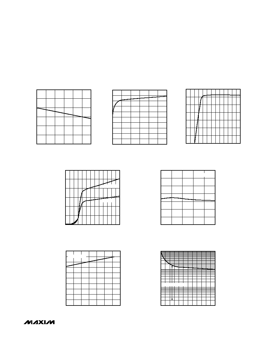
0.01
0
60
80
20
40
100
120
REGION OF STABLE C
OUT
ESR
vs. LOAD CURRENT
0.1
MAX1749 toc08
LOAD CURRENT (mA)
C
OUT
ESR (
)
1
10
STABLE REGION
0
40
20
80
60
100
120
0
1
2
3
4
5
6
SUPPLY CURRENT
vs. INPUT VOLTAGE
MAX1749 toc04
INPUT VOLTAGE (V)
SUPPLY CURRENT (
µ
A)
I
LOAD
= 50mA
I
LOAD
= 0
1.21
1.23
1.22
1.25
1.24
1.27
1.26
1.28
-40
10
-15
35
60
85
OUTPUT VOLTAGE
vs. TEMPERATURE
MAX1749 toc05
TEMPERATURE (°C)
OUTPUT VOLTAGE (V)
I
LOAD
= 50mA
0
10
20
30
40
50
60
70
80
90
100
100
80
60
40
20
0
-20
-40
SUPPLY CURRENT
vs. TEMPERATURE
MAX1749 toc06
TEMPERATURE (°C)
SUPPLY CURRENT (
µ
A)
I
LOAD
= 50mA
__________________________________________Typical Operating Characteristics
(V
IN
= +3.6V, SET = OUT, C
IN
= 1µF, C
OUT
= 1µF, T
A
= +25°C, unless otherwise noted.)
1.21
1.23
1.22
1.25
1.24
1.26
1.27
0
40
60
20
80
100
120
OUTPUT VOLTAGE
vs. LOAD CURRENT
MAX1749 TOC01
LOAD CURRENT (mA)
OUTPUT VOLTAGE (V)
0
30
20
10
40
50
60
70
80
90
100
0
40
20
60
80
100
120
SUPPLY CURRENT vs. LOAD CURRENT
MAX1749toc02
LOAD CURRENT (mA)
SUPPLY CURRENT (
µ
A)
0
0.4
0.2
0.6
0.8
1.0
1.2
1.4
0
1
2
3
4
5
6
OUTPUT VOLTAGE
vs. INPUT VOLTAGE
MAX1749toc03
INPUT VOLTAGE (V)
OUTPUT VOLTAGE (V)
MAX1749
SOT23 Vibrator Motor Driver
4
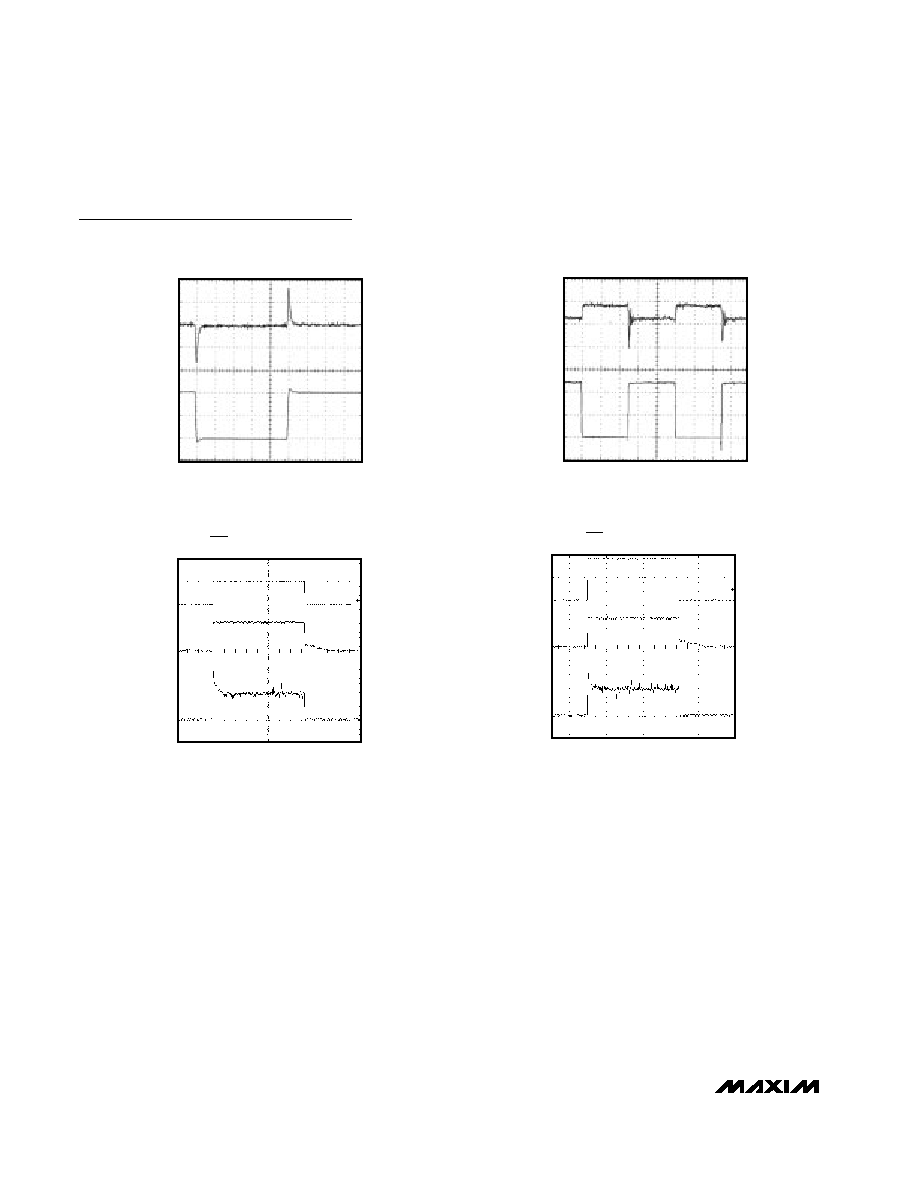
_______________________________________________________________________________________
I
LOAD
= 0 to 50mA, C
IN
= 10
µ
F, V
OUT
= AC-COUPLED
LOAD-TRANSIENT RESPONSE
1.25V
1.24V
1.23V
I
LOAD
20mA/div
10
µ
s/div
MAX1749 toc10
V
OUT
VIBRATOR MOTOR LOAD
ON/OFF WAVEFORM (V
IN
= 3.6V)
4V
2V
1V
200mA
0V
0V
0mA
I
LOAD
100ms/div
V
ON
V
OUT
MAX1749 toc14
I
LOAD
= 50mA, C
IN
= 10
µ
F, V
OUT
= AC-COUPLED
LINE-TRANSIENT RESPONSE
1.25V
1.24V
1.23V
4.6V
3.6V
V
IN
50
µ
s/div
MAX1749 toc09
V
OUT
VIBRATOR MOTOR LOAD
ON/OFF WAVEFORM (V
IN
= 5.0V)
5V
0V
1V
200mA
0V
0mA
I
LOAD
100ms/div
MAX1749 toc13
V
ON
V
OUT
Typical Operating Characteristics (continued)
(V
IN
= +3.6V, SET = OUT, C
IN
= 1µF, C
OUT
= 1µF, T
A
= +25°C, unless otherwise noted.)

MAX1749
SOT23 Vibrator Motor Driver
_______________________________________________________________________________________
5
Detailed Description
The MAX1749 is a low-quiescent-current, vibrator motor dri-
ver designed for battery-powered wireless handsets and
pagers. The device supplies an adjustable +1.25V to +6.5V
output for load currents up to 120mA. The MAX1749 allows
for a constant vibration force while operating from a +2.5V
to +6.5V input voltage range.
The 1.25V bandgap reference is connected to the error
amplifier's inverting input. The error amplifier compares this
reference with the feedback voltage and amplifies the differ-
ence. The MOSFET driver reads the error signal and
applies the appropriate drive to the p-channel pass transis-
tor. If the feedback voltage is lower than the reference volt-
age, the pass-transistor gate is pulled lower than the
reference, allowing more current to flow and increasing the
output voltage. If the feedback voltage is too high, the pass-
transistor gate is pulled-up, allowing less current to flow to
the output. The output voltage is fed back to SET either
directly for a 1.25V fixed output or through an external resis-
tor-divider for an adjustable +1.25V to V
IN
output. Additional
blocks include a current limiter, reverse battery protection, a
thermal sensor, and ON/ OFF logic.
Internal P-Channel Pass Transistor
The MAX1749 features a 1.1
typical P-channel MOS-
FET pass transistor. This provides several advantages
over similar designs using PNP pass transistors, includ-
ing longer battery life.
ON/OFF
LOGIC
ERROR
AMP
1.25V
REF
P
OUT
SET
GND
IN
ON
MAX1749
MOS DRIVER
WITH I
LIMIT
THERMAL
SENSOR
REVERSE
BATTERY
PROTECTION
______________________________________________________________Pin Description
Active-High On/Off Input. Apply a logic high to deliver power to the load. Apply a logic low to disconnect the
load and reduce the supply current to 0.1nA.
ON
1
PIN
FUNCTION
NAME
GND
2
Ground. This pin also functions as a heatsink. Solder to large pads or the circuit board ground plane to max-
imize thermal dissipation.
3
Regulator Input. Supply voltage can range from +2.5V to +6.5V. Bypass with 1µF to GND (see
Capacitor
Selection and Regulator Stability).
OUT
4
Regulator Output. Fixed 1.25V or adjustable from 1.25V to V
IN
. Sources up to 120mA. Bypass with a 1µF,
<0.2
typical ESR capacitor to GND.
IN
SET
5
Feedback Input for Setting the Output Voltage. Connect to OUT for 1.25V regulated output (see
Output
Voltage Selection). Connect to an external resistor-divider for adjustable-output operation.
Figure 1. Functional Diagram