General Description
The MAX1748 triple-output DC-DC converter in a low-
profile TSSOP package provides the regulated voltages
required by active matrix, thin-film transistor (TFT) liquid
crystal displays (LCDs). One high-power DC-DC con-
verter and two low-power charge pumps convert the
+3.3V to +5V input supply voltage into three independent
output voltages.
The primary high-power DC-DC converter generates a
boosted output voltage (V
MAIN
) up to 13V that is regu-
lated within ▒1%. The low-power BiCMOS control cir-
cuitry and the low on-resistance (0.35
) of the
integrated power MOSFET allows efficiency up to 93%.
The 1MHz current-mode PWM architecture provides
fast transient response and allows the use of ultra-small
inductors and ceramic capacitors.
The dual charge pumps independently regulate one
positive output (V
POS
) and one negative output (V
NEG
).
These low-power outputs use external diode and
capacitor stages (as many stages as required) to regu-
late output voltages up to +40V and down to -40V. A
proprietary regulation algorithm minimizes output rip-
ple, as well as capacitor sizes for both charge pumps.
The MAX1748 is available in the ultra-thin TSSOP pack-
age (1.1mm max height).
________________________Applications
TFT Active Matrix LCD Displays
Passive Matrix LCD Displays
PDAs
Digital Still Cameras
Camcorders
Features
o Three Integrated DC-DC Converters
o 1MHz Current-Mode PWM Boost Regulator
Up to +13V Main High-Power Output
▒1% Accuracy
High Efficiency (93%)
o Dual Charge-Pump Outputs
Up to +40V Positive Charge-Pump Output
Down to -40V Negative Charge-Pump Output
o Internal Supply Sequencing
o Internal Power MOSFETs
o +2.7V to +5.5V Input Supply
o 0.1ÁA Shutdown Current
o 0.6mA Quiescent Current
o Internal Soft-Start
o Power-Ready Output
o Ultra-Small External Components
o Thin TSSOP Package (1.1mm max)
MAX1748
Triple-Output TFT LCD DC-DC Converter
________________________________________________________________ Maxim Integrated Products
1
16
15
14
13
12
11
10
9
1
2
3
4
5
6
7
8
RDY
TGND
LX
PGND
SUPP
DRVP
SUPN
DRVN
SHDN
TOP VIEW
MAX1748
TSSOP
FB
INTG
REF
IN
GND
FBP
FBN
Pin Configuration
19-1740; Rev 0; 6/00
For free samples and the latest literature, visit www.maxim-ic.com or phone 1-800-998-8800.
For small orders, phone 1-800-835-8769.
Ordering Information
Typical Operating Circuit appears at end of data sheet.
16 TSSOP
PIN-PACKAGE
TEMP. RANGE
-40░C to +85░C
MAX1748EUE
PART
MAX1748
Triple-Output TFT LCD DC-DC Converter
2
_______________________________________________________________________________________
ABSOLUTE MAXIMUM RATINGS
ELECTRICAL CHARACTERISTICS
(V
IN
= +3.0V, SHDN = IN, V
SUPP
= V
SUPN
= 10V, TGND = PGND = GND, C
REF
= 0.22ÁF, C
INTG
= 470pF, T
A
= 0░C to +85░C, unless
otherwise noted. Typical values are at T
A
= +25░C.)
Stresses beyond those listed under "Absolute Maximum Ratings" may cause permanent damage to the device. These are stress ratings only, and functional
operation of the device at these or any other conditions beyond those indicated in the operational sections of the specifications is not implied. Exposure to
absolute maximum rating conditions for extended periods may affect device reliability.
IN, SHDN, TGND to GND .........................................-0.3V to +6V
DRVN to GND .........................................-0.3V to (V
SUPN
+ 0.3V)
DRVP to GND..........................................-0.3V to (V
SUPP
+ 0.3V)
PGND to GND.....................................................................▒0.3V
RDY to GND ...........................................................-0.3V to +14V
LX, SUPP, SUPN to PGND .....................................-0.3V to +14V
INTG, REF, FB, FBN, FBP to GND ...............-0.3V to (V
IN
+ 0.3V)
Continuous Power Dissipation (T
A
= +70░C)
16-Pin TSSOP (derate 9.4mW/░C above +70░C) ..........755mW
Operating Temperature Range
MAX1748EUE .................................................-40░C to +85░C
Junction Temperature ......................................................+150░C
Storage Temperature Range .............................-65░C to +150░C
Lead Temperature (soldering, 10s) .................................+300░C
PARAMETER
SYMBOL
CONDITIONS
MIN
TYP
MAX
UNITS
Input Supply Range
V
IN
2.7
5.5
V
Input Undervoltage Threshold
V
UVLO
V
IN
rising, 40mV hysteresis (typ)
2.2
2.4
2.6
V
IN Quiescent Supply Current
I
IN
V
FB
= V
FBP
= 1.5V, V
FBN
= -0.2V
0.6
1
mA
SUPP Quiescent Current
I
SUPP
V
FBP
= 1.5V
0.4
0.8
mA
SUPN Quiescent Current
I
SUPN
V
FBN
= -0.1V
0.4
0.8
mA
IN Shutdown Current
V
SHDN
= 0, V
IN
= 5V
0.1
10
ÁA
SUPP Shutdown Current
V
SHDN
= 0, V
SUPP
= 13V
0.1
10
ÁA
SUPN Shutdown Current
V
SHDN
= 0, V
SUPN
= 13V
0.1
10
ÁA
MAIN BOOST CONVERTER
Output Voltage Range
V
MAIN
V
IN
13
V
FB Regulation Voltage
V
FB
T
A
= 0
░C to +85░C
1.235
1.248
1.261
V
FB Input Bias Current
I
FB
V
FB
= 1.25V, INTG = GND
-50
50
nA
Operating Frequency
f
OSC
0.85
1
1.15
MHz
Oscillator Maximum Duty Cycle
78
85
90
%
Load Regulation
I
MAIN
= 0 to 200mA, V
MAIN
= 10V
0.2
%
Line Regulation
0.1
% / V
Integrator Gm
320
Ámho
LX Switch On-Resistance
R
LX(ON)
I
LX
= 100mA
0.35
0.7
LX Leakage Current
I
LX
V
LX
= 13V
0.01
20
ÁA
Phase I = soft-start (1.0ms)
0.275
0.380
0.500
Phase II = soft-start (1.0ms)
0.75
Phase III = soft-start (1.0ms)
1.12
LX Current Limit
I
LX(MAX)
Phase IV = fully on (after 3.0ms)
1.1
1.5
2.0
A
Maximum RMS LX Current
1
A
Soft-Start Period
t
SS
Power-up to the end of Phase III
3072 /
f
OSC
s
FB Fault Trip Level
1.07
1.1
1.14
V
POSITIVE CHARGE PUMP
V
SUPP
Input Supply Range
V
SUPP
2.7
13
V
MAX1748
Triple-Output TFT LCD DC-DC Converter
_______________________________________________________________________________________
3
ELECTRICAL CHARACTERISTICS (continued)
(V
IN
= +3.0V, SHDN = IN, V
SUPP
= V
SUPN
= 10V, TGND = PGND = GND, C
REF
= 0.22ÁF, C
INTG
= 470pF, T
A
= 0░C to +85░C, unless
otherwise noted. Typical values are at T
A
= +25░C.)
PARAMETER
SYMBOL
CONDITIONS
MIN
TYP
MAX
UNITS
Operating Frequency
0.5
Î
f
OSC
Hz
FBP Regulation Voltage
V
FBP
1.20
1.25
1.30
V
FBP Input Bias Current
I
FBP
V
FBP
= 1.5V
-50
50
nA
DRVP PCH On-Resistance
3
10
V
FBP
= 1.213V
1.5
4
DRVP NCH On-Resistance
V
FBP
= 1.275V
20
k
FBP Power-Ready Trip Level
Rising edge
1.091
1.125
1.159
V
FBP Fault Trip Level
Falling edge
1.11
V
Maximum RMS DRVP Current
0.1
A
NEGATIVE CHARGE PUMP
V
SUPN
Input Supply Range
V
SUPN
2.7
13
V
Operating Frequency
0.5
Î
f
OSC
Hz
FBN Regulation Voltage
V
FBN
-50
0
50
mV
FBN Input Bias Current
I
FBN
V
FBN
= -0.05V
-50
50
nA
DRVN PCH On-Resistance
3
10
V
FBN
= 0.035V
1.5
4
DRVN NCH On-Resistance
V
FBN
= -0.025V
20
k
FBN Power-Ready Trip Level
Rising edge
80
110
165
mV
FBN Fault Trip Level
Falling edge
130
mV
Maximum RMS DRVN Current
0.1
A
REFERENCE
Reference Voltage
V
REF
-2ÁA < I
REF
< 50ÁA
1.231
1.25
1.269
V
Reference Undervoltage
Threshold
V
REF
rising
0.9
1.05
1.2
V
LOGIC SIGNALS
SHDN Input Low Voltage
0.4V hysteresis (typ)
0.9
V
SHDN Input High Voltage
2.1
V
SHDN Input Current
I
SHDN
0.01
1
ÁA
RDY Output Low Voltage
I
SINK
= 2mA
0.25
0.5
V
RDY Output High Voltage
V
RDY
= 13V
0.01
1
ÁA

MAX1748
Triple-Output TFT LCD DC-DC Converter
4
_______________________________________________________________________________________
PARAMETER
SYMBOL
CONDITIONS
MIN
MAX
UNITS
Input Supply Range
V
IN
2.7
5.5
V
Input Undervoltage Threshold
V
UVLO
V
IN
rising, 40mV hysteresis (typ)
2.2
2.6
V
IN Quiescent Supply Current
I
IN
V
FB
= V
FBP
= 1.5V, V
FBN
= -0.2V
1
mA
SUPP Quiescent Current
I
SUPP
V
FBP
= 1.5V
0.8
mA
SUPN Quiescent Current
I
SUPN
V
FBN
= -0.1V
0.8
mA
IN Shutdown Current
V
SHDN
= 0, V
IN
= 5V
10
ÁA
SUPP Shutdown Current
V
SHDN
= 0, V
SUPP
= 13V
10
ÁA
SUPN Shutdown Current
V
SHDN
= 0, V
SUPN
= 13V
10
ÁA
MAIN BOOST CONVERTER
Output Voltage Range
V
MAIN
V
IN
13
V
FB Regulation Voltage
V
FB
1.225
1.271
V
FB Input Bias Current
I
FB
V
FB
= 1.25V, INTG = GND
-50
50
nA
Operating Frequency
F
OSC
0.75
1.25
MHz
Oscillator Maximum Duty Cycle
78
90
%
LX Switch On-Resistance
R
LX(ON)
I
LX
= 100mA
0.7
LX Leakage Current
I
LX
V
LX
= 13V
20
ÁA
Phase I = soft-start (1.0ms)
0.275
0.500
LX Current Limit
I
LX(MAX)
Phase IV = fully on (after 3.0ms)
1.1
2.0
A
FB Fault Trip Level
1.07
1.14
V
POSITIVE CHARGE PUMP
SUPP Input Supply Range
V
SUPP
2.7
13
V
FBP Regulation Voltage
V
FBP
1.20
1.30
V
FBP Input Bias Current
I
FBP
V
FBP
= 1.5V
-50
50
nA
DRVP PCH On-Resistance
10
V
FBP
= 1.213V
4
DRVP NCH On-Resistance
V
FBP
= 1.275V
20
k
FBP Power-Ready Trip Level
Rising edge
1.091
1.159
V
NEGATIVE CHARGE PUMP
SUPN Input Supply Range
V
SUPN
2.7
13
V
FBN Regulation Voltage
V
FBN
-50
50
mV
FBN Input Bias Current
I
FBN
V
FBN
= -0.05V
-50
50
nA
DRVN PCH On-Resistance
10
V
FBN
= 0.035V
4
DRVN NCH On-Resistance
V
FBN
= -0.025V
20
k
FBN Power-Ready Trip Level
Rising edge
80
165
mV
REFERENCE
Reference Voltage
V
REF
-2
ÁA < I
REF
< 50
ÁA
1.223
1.269
V
Reference Undervoltage
V
REF
rising
0.9
1.2
V
ELECTRICAL CHARACTERISTICS (continued)
(V
IN
= +3.0V, SHDN = IN, V
SUPP
= V
SUPN
= 10V, TGND = PGND = GND, C
REF
= 0.22ÁF, C
INTG
= 470pF, T
A
= -40░C to +85░C,
unless otherwise noted.) (Note 1)
MAX1748
Triple-Output TFT LCD DC-DC Converter
_______________________________________________________________________________________
5
9.84
9.90
9.88
9.86
9.92
9.94
9.96
9.98
10.00
10.02
10.04
0
200
100
300
400
500
600
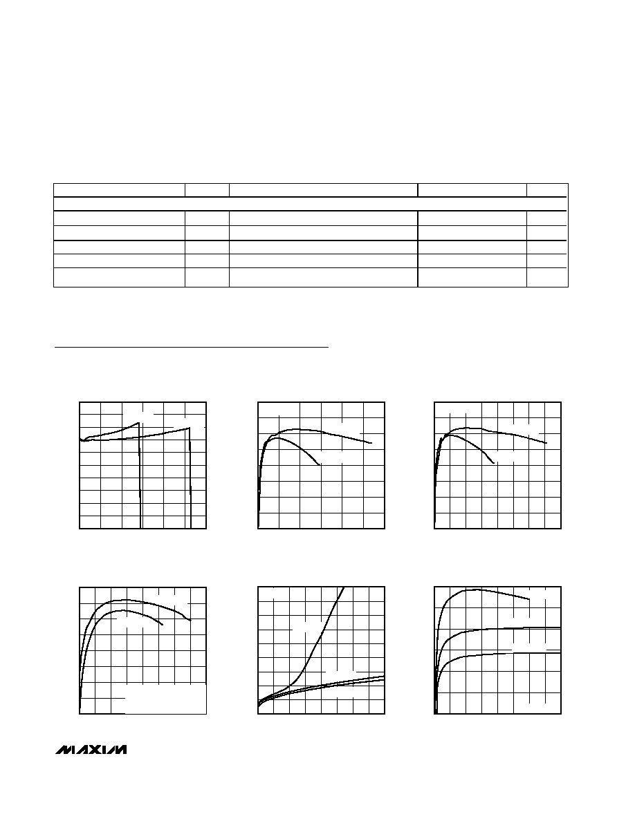
MAIN OUTPUT VOLTAGE
vs. LOAD CURRENT
MAX1748 toc01
I
MAIN
(mA)
V
MAIN
(V)
V
IN
= 3.3V
V
IN
= 5.0V
60
65
70
75
80
85
90
95
100
0
200
100
300
400
500
600
MAIN STEP-UP CONVERTER
EFFICIENCY vs. LOAD CURRENT
(BOOST ONLY)
MAX1748toc02
I
MAIN
(mA)
EFFICIENCY (%)
V
IN
= 3.3V
V
MAIN
= 10V
V
IN
= 5.0V
60
65
70
75
80
85
90
95
100
0
200
100
300 400
500
800
600
700
MAIN STEP-UP CONVERTER
EFFICIENCY vs. LOAD CURRENT
(BOOST ONLY)
MAX1748toc03
I
MAIN
(mA)
EFFICIENCY (%)
V
IN
= 3.3V
V
MAIN
= 8V
V
IN
= 5.0V
50
55
60
65
70
75
80
85
90
0
100
50
150 200
250
400
300
350
EFFICIENCY vs. LOAD CURRENT
(BOOST CONVERTER AND CHARGE PUMPS)
MAX1748toc04
I
MAIN
(mA)
EFFICIENCY (%)
V
MAIN
= 8V
V
IN
= 3.3V
V
NEG
= -5V WITH I
NEG
= 10mA
V
POS
= 15V WITH I
POS
= 5mA
V
MAIN
= 10V
-5.05
-4.95
-5.00
-4.80
-4.85
-4.90
-4.65
-4.70
-4.75
-4.60
0
15
20
5
10
25
30
35
40
NEGATIVE CHARGE-PUMP OUTPUT
VOLTAGE vs. LOAD CURRENT
MAX1748toc05
I
NEG
(mA)
V
NEG
(V)
V
SUPN
= 6V
V
NEG
= -5V
V
SUPN
= 8V
V
SUPN
= 10V
20
30
50
40
70
60
80
0
15
20
5
10
25
30
35
40
NEGATIVE CHARGE-PUMP EFFICIENCY
vs. LOAD CURRENT
MAX1748toc06
I
NEG
(mA)
EFFICIENCY (%)
V
SUPN
= 6V
V
NEG
= -5V
V
SUPN
= 8V
V
SUPN
= 10V
Typical Operating Characteristics
(Circuit of Figure 5, V
IN
= 3.3V, T
A
= +25░C, unless otherwise noted.)
ELECTRICAL CHARACTERISTICS (continued)
(V
IN
= +3.0V, SHDN = IN, V
SUPP
= V
SUPN
= 10V, TGND = PGND = GND, C
REF
= 0.22ÁF, C
INTG
= 470pF, T
A
= -40░C to +85░C,
unless otherwise noted.) (Note 1)
PARAMETER
SYMBOL
CONDITIONS
MIN
MAX
UNITS
LOGIC SIGNALS
SHDN Input Low Voltage
0.45V hysteresis (typ)
0.9
V
SHDN Input High Voltage
2.1
V
SHDN Input Current
I
SHDN
1
ÁA
RDY Output Low Voltage
I
SINK
= 2mA
0.5
V
RDY Output High Leakage
V
RDY
= 13V
1
ÁA
Note 1: Specifications from 0░C to -40░C are guaranteed by design, not production tested.