19-2870; Rev 0; 04/03
MAXIM
MAX1
MAX1544/MAX1545 Evaluation Kits
544/MAX1545 Evaluation Kits
MAXIM
Maxim Integrated Products 1
For pricing, delivery, and ordering information, please contact Maxim/Dallas Direct! at
1-888-629-4642, or visit Maxim's website at www.maxim-ic.com.
________________________________________________________
________________________________________________________
General Description
General Description
The MAX1544/MAX1545 evaluation kits (EV kits)
demonstrate the high-power, dynamically adjustable
multiphase notebook CPU application circuit. This DC-DC
converter steps down high-voltage batteries and/or AC
adapters, generating a precision, low-voltage CPU core
VCC rail. The MAX1544 EV kit meets the mobile and
desktop AMD Hammer CPU transient voltage
specification. The MAX1545 EV kit meets the desktop and
mobile Pentium 4 (P4) CPUs transient voltage
specification. The MAX1544/MAX1545 kits consist of the
MAX1544 or MAX1545 Dual-Phase Quick-PWMTM step-
down controller, two MAX1980 slave controllers and the
MAX6590 temperature sensor. The MAX1544/MAX1545
kits include active voltage positioning with adjustable gain
and offset, reducing power dissipation and bulk output
capacitance requirements. The kit features independent
four-level logic inputs for setting the suspend voltage
(S0/S1).
The MAX1980 provides additional gate drive circuitry,
phase synchronization, current limit, and current
balancing. Precision slew-rate control provides "just-in
time" arrival at the new DAC setting, minimizing surge
currents to and from the battery.
This fully assembled and tested circuit board provides a 5-
bit digitally adjustable output voltage from a 7V to 24V
battery input range. The EV kit operates at 300kHz
switching frequency and has superior line- and load-
transient response.
Pentium is a registered trademark of Intel Corp.
Hammer is a trademark of Advanced Micro Devices, Inc.
QuickPWM is a trademark of Maxim Integrated Products, Inc.
_________________________________________________________________________________________
_________________________________________________________________________________________
Features
Features
Quad-Phase Quick-PWM
TM
EV Kit
Mobile and Desktop P4 or AMD Hammer
Compatible
Active Voltage Positioning with Adjustable Gain,
Offset and Remote Sensing
High Speed, Accuracy and Efficiency
Low Bulk Output Capacitor Count
Multiphase Fast-Response Quick-PWM
Architecture
MAX1544/MAX1545 Dual-Phase Controller
Two MAX1980 Slave Controllers
7V to 24V Input Voltage Range
5-Bit On-Board DAC
Mobile P4: 0.60V to 1.75V Output Range
Desktop P4: 1.10V to 1.85V Output Range
AMD Hammer: 0.675V to 1.55V Output Range
68A Load-Current Capability (17A Each Phase)
300kHz Switching Frequency
MAX6509 Temperature Sensor
40-Pin Thin QFN Package (MAX1544/MAX1545)
20-Pin Thin QFN Package (MAX1980)
Fully Assembled and Tested
___________________________________
___________________________________
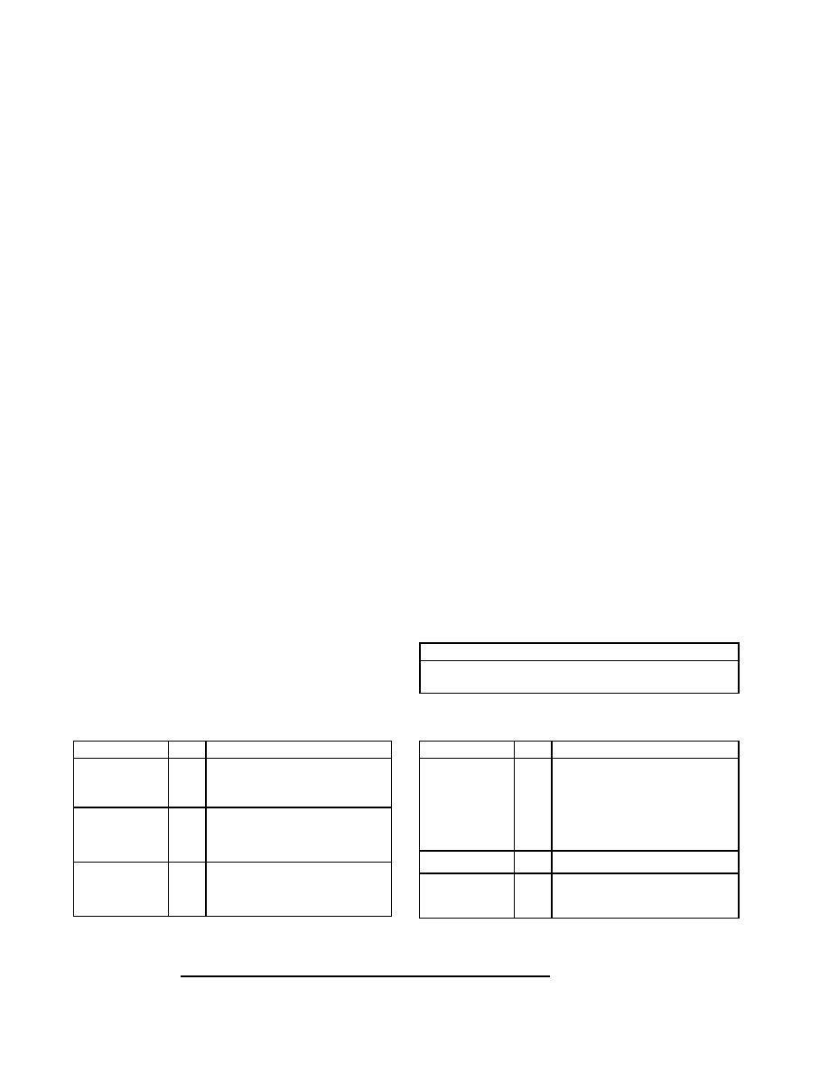
Ordering Information
Ordering Information
PART
TEMP RANGE
IC PACKAGE
MAX1544EVKIT
MAX1545EVKIT
0
�
C to +70
�
C
40 QFN (MAX154_)
20 QFN (MAX1980)
Evaluates: MAX1544/MAX1545
Evaluates: MAX1544/MAX1545
___________________________________________________________________________________________________________________________________
___________________________________________________________________________________________________________________________________
Component List
Component List
DESIGNATION
QTY
DESCRIPTION
C1-C4, C7, C20,
C25, C26, C33,
C35, C62, C64
0
Not Installed (0603)
C5, C24, C36,
C49
4
100pF 5% 50V C0G ceramic
capacitor (0603)
Murata GRM1885C1H101J
C6, C21, C23,
C38, C39, C51,
C60
7
0.22�F 16V X5R ceramic capacitor
(0805)
Taiyo Yuden EMK212BJ224KG
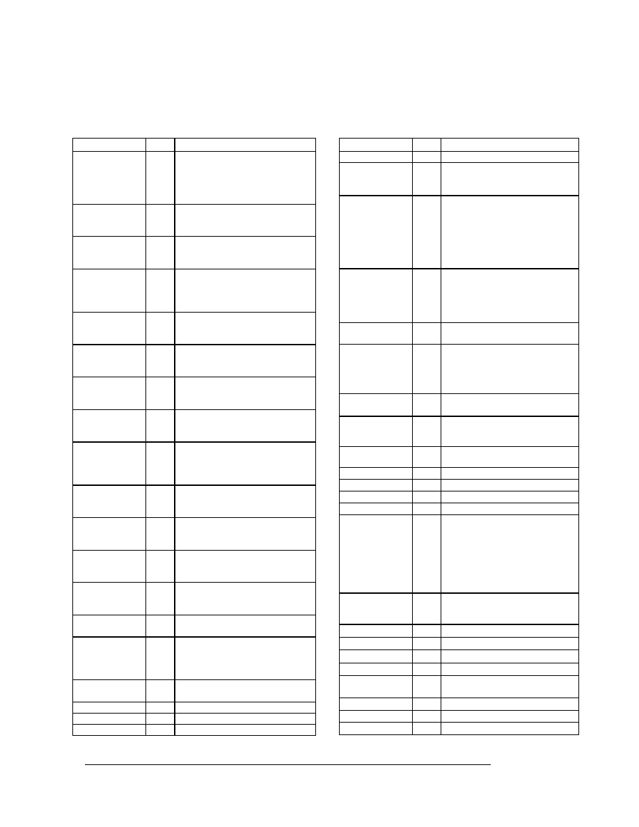
DESIGNATION
QTY
DESCRIPTION
C8-C12, C31,
C32, C47
8
330�F, 2.5V 9m
Low-ESR
polymer capacitor (D case)
Sanyo 2R5TPE330M9
or
or
C8-C12, C31,
C32, C47
8
330�F, 2V 7m
Low-ESR specialty
polymer capacitor (D case)
Panasonic EEFSD0D331XR
C13
0
Not installed (E case)
C14, C29, C58,
C59
4
1000pF 10% 50V C0G ceramic
capacitor (0603)
Murata GRM188R71H102K
MAX1
MAX1544/
544/MAX1545 Evaluation Kits
MAX1545 Evaluation Kits
2
MAXIM
________________________________________________________________________________________________________
________________________________________________________________________________________________________
Component List (continued)
Component List (continued)
Evaluates: MAX1544/MAX1545
Evaluates: MAX1544/MAX1545
DESIGNATION
QTY
DESCRIPTION
C15, C22, C34,
C45
4
4700pF 10% 50V X7R ceramic
capacitor (0603)
Murata GRM188R71H472K
(Not installed when using
Si7442DP)
C16
1
2.2�F 10V X5R ceramic capacitor
(0612)
TDK C1632X5R1A225KTB09N
C17, C18, C19,
C41, C42, C43,
C53, C54, C65
9
15�F 20% 25V X5R ceramic
capacitor (1812)
TDK C4532X5R1E156M
C27, C40, C52
3
1�F 20% 10V X5R ceramic
capacitor (0805)
Taiyo Yuden LMK212BJ105KG or
TDK C2012X7R1C105MKT
C28
1
47pF 5% 50V C0G ceramic
capacitor (0603)
Murata GRM1885C1H470J
C30, C37, C50,
C56, C63
5
470pF 10% 50V X7R ceramic
capacitor (0603)
Murata GRM188R71H471K
C44, C48, C55,
C57
4
1�F 10% 25V X7R ceramic
capacitor (0805)
TDK C2012X7R1E105K
C61
1
0.1�F 10% 50V X7R ceramic
capacitor (0805)
Murata GRM21BR71H104K
C67, C69, C70,
C83, C84, C85,
C87, C97-C101
12
10�F 20% 6.3V X5R ceramic
capacitor (0805)
TDK C2012X5R0J106M or
Taiyo Yuden AMK212BJ106MG
C71-C78, C80-
C82, C88-C92
16
22�F 6.3V X5R ceramic capacitor
(1206)
TDK C3216X5R0J226MT
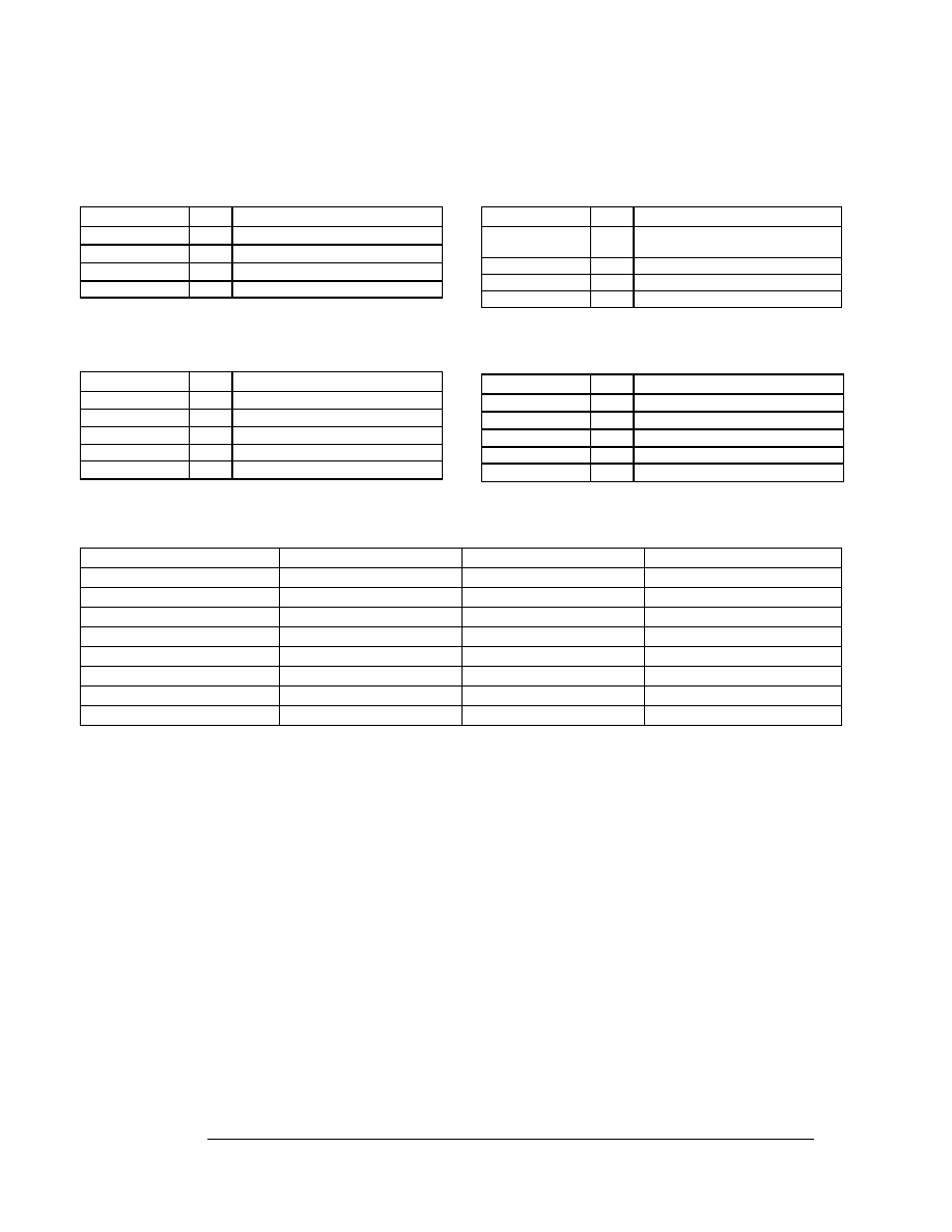
D1
1
100mA, 30V Dual Schottky Diode
Central Semiconductor
CMPSH-3A
D2, D3, D4, D12
4
5A Schottky Diode
Central Semiconductor
CMSH5-40
D5, D13
2
100mA, 30V Schottky Diode
Central Semiconductor
CMPSH-3
D6, D11
2
200mA Switching Diode
Central Semiconductor CMPD2838
D7, D10
0
Not Installed
100mA, 30V Dual Schottky Diode
Central Semiconductor
CMPSH-3C
J2
1
4-pin header
Molex 39-29-3046
JUA0-JUA5
6
2-pin header
JU1, JU3, JU4
3
4-pin header
JU13
0
2-pin header
DESIGNATION
QTY
DESCRIPTION
JU2
1
3-pin header
L1-L4
4
0.6�H 26A 0.9m
Power Inductors
Panasonic ETQP1H0R6BFA or
Sumida CDEP134H-0R6
N1, N2, N5, N6,
N7, N10, N15,
N16
8
N-channel MOSFET (SO-8)
International Rectifier IRF7811W
or
Fairchild FDS6694
or
or
N2, N7, N10,
N16
4
Vishay/Siliconix Si7886DP
(Power PAK)
N3, N4, N8, N9,
N11, N12, N13,
N14
8
N-channel MOSFET (SO-8)
International Rectifier IRF7822 or
Fairchild FDS6688 or
Vishay/Siliconix Si7442DP
(Power PAK)
Q1, Q2
2
N-channel MOSFET
Central Semiconductor 2N7002
R1, R8, R11,
R14, R15, R17,
R20, R37, R50,
R52, R63, R64,
R78, R98, R102
0
Not Installed, (short PC trace)
(0603)
R2, R9, R39,
R45
4
0.001
�1% 1W resistor (2512)
Panasonic ERJM1WTF1M0U
R3, R33-R35,
R40, R44, R46,
R48, R49, R107
10
100
�5% resistor (0603)
R5, R6, R18,
R24
4
1k
�1% resistor (0603)
R7
1
60.4k
�1% resistor (0603)
R10
1
100k
�1% resistor (0603)
R12
1
20k
�1% resistor (0603)
R16, R83, R84
3
10
�5% resistor (0603)
R19, R21, R27,
R30, R36, R51,
R53, R61, R62,
R65-R67, R74,
R75, R81, R87,
R92, R99-R101,
R103-R106,
R108, R109
0
Not Installed (0603)
R26, R28, R73,
R76, R77, R79,
R80
7
0
�5% resistor (0603)
R29, R31
2
30.1k
�1% resistor (0603)
R32, R42
2
150k
�1% resistor (0603)
R41, R47
2
20
�5% resistor (0603)
R43, R38
2
10k
�5% resistor (0603)
R54-R59, R70,
R95-R97, R110
11
100k
�5% resistor (0603)
R60
1
11k
�1% resistor (0603)
R82
1
1M
�5% resistor (0603)
U2, U3
2
MAX1980ETP (20-TQFN)
MAX1
MAX1544/MAX1545 Evaluation Kits
544/MAX1545 Evaluation Kits
MAXIM
3
________________________________________________________________________________
________________________________________________________________________________
Quick Start
Quick Start
Recommended Equipment
�
7V to 24V, >100W power supply, battery, or notebook
AC adapter
�
DC bias power supply, 5V at 1A
�
One or more dummy loads capable of sinking 68A total
�
Digital multimeter (DMM)
�
100MHz dual-trace oscilloscope
Procedure
1) Ensure that the circuit is connected correctly to the
supplies and dummy load prior to applying any power.
2) Verify that the shunts are across JU1 pins 1 and 3 (S0)
and JU3 pins 1 and 4 (S1), JU2 pins 1 and 2 (
SHDN
)
and JU4 pins 1 and 3 (TON). The DAC code settings
(D4�D0) are set for 1.50V output through installed
jumpers JUA3 and JUA1. A fixed +50mV offset fsets the
final no load output voltage at 1.55V for the MAX1544
EV kit. A fixed -25mV offset sets the final no load output
voltage at 1.45V for the MAX5145 EV kit.
3) Turn on the battery power before turning on the +5V bias
power; otherwise, the output UVLO timer times out and
the FAULT latch is set, disabling the regulator until +5V
power is cycled or shutdown is toggled.
4) Observe the output voltage with the DMM and/or
oscilloscope. Look at the LX switching nodes and
MOSFET gate-drive signals while varying the load
current.
_____________________________________________________
_____________________________________________________
Detailed Description
Detailed Description
This 68A multiphase buck-regulator design is optimized for a
300kHz frequency and output voltage settings from 1.0V to
1.5V. At VOUT=1.5V and VIN=12V, the inductor ripple is
approximately 30% (LIR=0.3). The MAX1544/MAX1545
controller shares the current between its two phases that
operate 180� out-of-phase, supplying 17A per phase. Each
MAX1980 slave is triggered by one side of the
MAX1544/MAX1545 low-side gate driver, supplying another
17A per slave.
__________________________________________________________________________________________________________
__________________________________________________________________________________________________________
Component List (continued)
Component List (continued)
DESIGNATION
QTY
DESCRIPTION
U4
1
MAX6509HAUK-T (5-SOT23)
U5
0
MAX6509HAUK-T (5-SOT23)
None
10
Shunts
None
1
MAX1544/MAX1545 PC Board
MAX1544 EV Kit
MAX1544 EV Kit
_____________________________
_____________________________
Additional Components
Additional Components
DESIGNATION
QTY
DESCRIPTION
R4, R23
2
2.61k
�1% resistor (0603)
R22
1
24.9k
�1% resistor (0603)
R25
1
100k
�1% resistor (0603)
U1
1
MAX1544ETL (40-TQFN)
U8
1
Socket 754
DESIGNATION
QTY
DESCRIPTION
None
1
MAX1544/MAX1545 EV kit data
sheet
None
1
MAX1544/MAX1545 data sheet
None
1
MAX1980 data sheet
None
1
MAX6509 data sheet
MAX1545 EV Kit
MAX1545 EV Kit
__________________________
__________________________
Additional Components*
Additional Components*
DESIGNATION
QTY
DESCRIPTION
R4, R23
2
3.01k
�1% resistor (0603)
R22
1
182k
�1% resistor (0603)
R25
1
20k
�1% resistor (0603)
U1
1
MAX1545ETL (40-TQFN)
U8
1
None
*Contact Intel for the Mobile P4 specifications and contact
Maxim for a reference schematic.
_______________________________________________________________________________________________________________________
_______________________________________________________________________________________________________________________
Component Suppliers
Component Suppliers
SUPPLIER
PHONE
FAX
WEBSITE
Central Semiconductor
516-435-1110
516-435-1824
www.centralsemi.com
Fairchild Semiconductor
408-721-2181
408-721-1635
www.fairchildsemi.com
International Rectifier
310-322-3331
310-322-3332
www.irf.com
Panasonic
714-373-7939
714-373-7183
www.panasonic.com
Sumida
708-956-0666
708-956-0702
www.sumida.com
Taiyo Yuden
408-573-4150
408-573-4159
www.t-yuden.com
TDK
847-390-4373
847-390-4428
www.component.tdk.com
Vishay/Siliconix
203-268-6261
203-268-6296
www.vishay.com
Note: Please indicate that you are using the MAX1544 and MAX1545 when contacting these component suppliers.
Evaluates: MAX1544/MAX1545
Evaluates: MAX1544/MAX1545
MAX1
MAX1544/
544/MAX1545 Evaluation Kits
MAX1545 Evaluation Kits
4
MAXIM
Setting the Output Voltage
The MAX1544/MAX1545 has two unique internal VID input
multiplexers that can select one of three different VID DAC
code settings for different processor states. On startup, the
controller selects the DAC code from the D0�D4 input
decoder when SUS=GND. A second multiplexer selects the
lower S0-S1 DAC code when SUS is high (SUS=3.3V or
VCC), or the higher S0-S1 DAC code when SUS=REF. The
output voltage can be digitally set by the D0-D4 pins (Table
1) or the S0-S1 pins (Table 2).
There are five different ways of setting the output voltage:
1) Drive the external VID0�VID4 inputs (no jumpers
installed): The output voltage can be set by driving
VID0�VID4 with open-drain drivers (pullup resistors are
included on the board) or 3V/5V CMOS output logic
levels (DPSLPVR = GND).
2) Install jumpers JUA0�JUA4: SUS=low. When JUA0�
JUA4 are not installed, the MAX1544/MAX1545's D0�
D4 inputs are at logic 1 (connected to VID_VCC). When
JUA0�JUA4 are installed, D0�D4 inputs are at logic 0
(connected to GND). The output voltage can be
changed during operation by installing and removing
jumpers JUA0�JUA4. As shipped, the EV kit is
configured with jumpers JUA0�JUA4 set for 1.50V
output (Table 1). Refer to the MAX1544 and MAX1545
data sheets for more information.
3) Drive DPSLPVR (suspend mode configuration): As
shipped, the EV kit is configured for operation in the
suspend mode S0-S1 set for 1.000V output (Table 2).
4) Drive
DPSLP
DPSLP
:
DPSLP
can be driven by an external
driver to introduce offsets to the output voltage (Table
2).
5) Drive header J1 for full system control: VID0-VID4,
DPSLP
, DPRSLPVR, VRON, and VROK are all
available directly on header connections J1 (Figure 1c).
Do not install jumper JU2 in this mode.
Evaluates: MAX1544/MAX1545
Evaluates: MAX1544/MAX1545
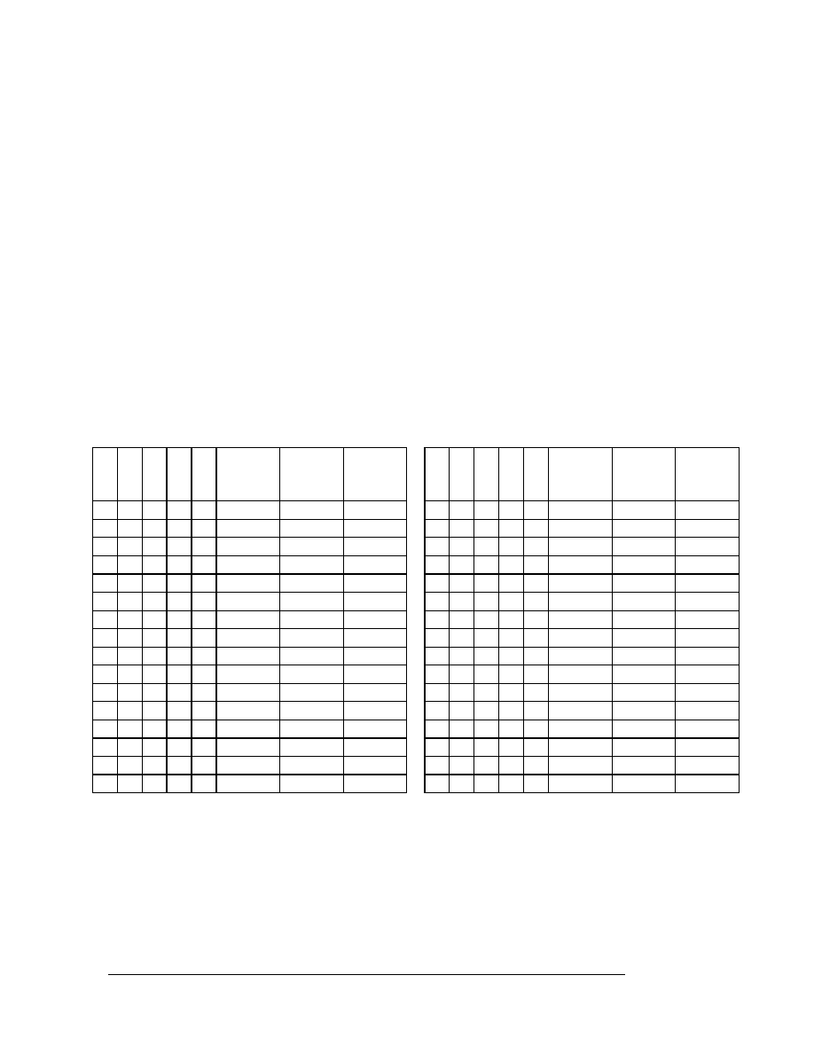
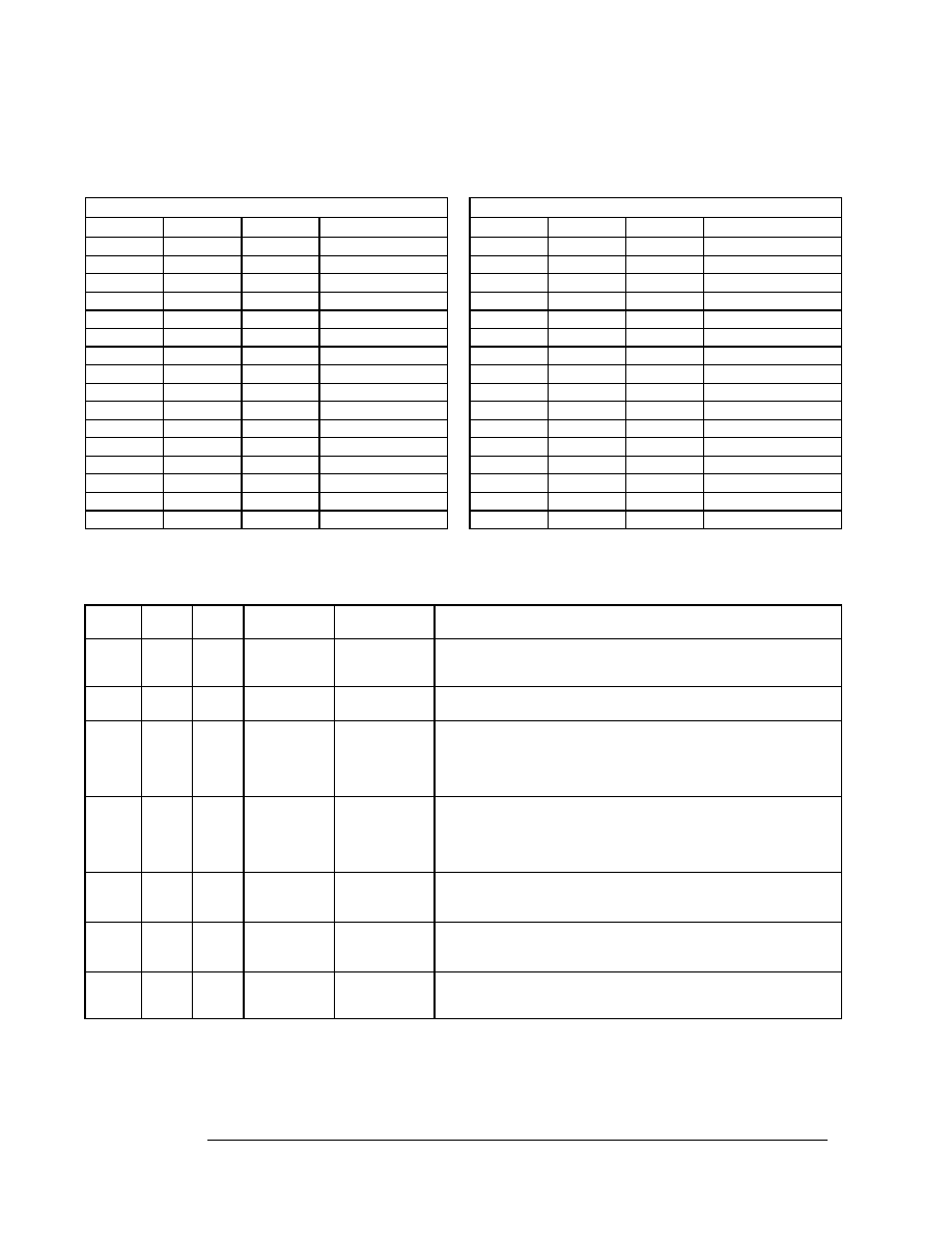
Table 1. MAX1544/MAX1545 Output Voltage Adjustment Settings (SUS=GND)
D4 D3 D2 D1 D0
MAX1544
VOUT (V)
MAX1545
CODE=VCC
VOUT (V)
MAX1545
CODE=GND
VOUT (V)
D4 D3 D2 D1 D0
MAX1544
VOUT (V)
MAX1545
CODE=VCC
VOUT (V)
MAX1545
CODE=GND
VOUT (V)
0
0
0
0
0
1.550
1.750
1.850
1
0
0
0
0
1.150
0.975
1.450
0
0
0
0
1
1.525
1.700
1.825
1
0
0
0
1
1.125
0.950
1.425
0
0
0
1
0
1.500
1.650
1.800
1
0
0
1
0
1.100
0.925
1.400
0
0
0
1
1
1.475
1.600
1.775
1
0
0
1
1
1.075
0.900
1.375
0
0
1
0
0
1.450
1.550
1.750
1
0
1
0
0
1.050
0.875
1.350
0
0
1
0
1
1.425
1.500
1.725
1
0
1
0
1
1.025
0.850
1.325
0
0
1
1
0
1.400
1.450
1.700
1
0
1
1
0
1.000
0.825
1.300
0
0
1
1
1
1.375
1.400
1.675
1
0
1
1
1
0.975
0.800
1.275
0
1
0
0
0
1.350
1.350
1.650
1
1
0
0
0
0.950
0.775
1.250
0
1
0
0
1
1.325
1.300
1.625
1
1
0
0
1
0.925
0.750
1.225
0
1
0
1
0
1.300
1.250
1.600
1
1
0
1
0
0.900
0.725
1.200
0
1
0
1
1
1.275
1.200
1.575
1
1
0
1
1
0.875
0.700
1.175
0
1
1
0
0
1.250
1.150
1.550
1
1
1
0
0
0.850
0.675
1.150
0
1
1
0
1
1.225
1.100
1.525
1
1
1
0
1
0.825
0.650
1.125
0
1
1
1
0
1.200
1.050
1.500
1
1
1
1
0
0.800
0.625
1.100
0
1
1
1
1
1.175
1.000
1.475
1
1
1
1
1
OFF
0.600
OFF
MAX1
MAX1544/MAX1545 Evaluation Kits
544/MAX1545 Evaluation Kits
MAXIM
5
Table 2. MAX1544/MAX1545 Output Voltage Adjustment Settings (SUS=High or REF)
LOWER SUSPEND CODES
UPPER SUSPEND CODES
SUS*
S1
S0
VOUT (V)
SUS*
S1
S0
VOUT (V)
High
GND
GND
0.675
REF
GND
GND
1.075
High
GND
REF
0.700
REF
GND
REF
1.100
High
GND
OPEN
0.725
REF
GND
OPEN
1.125
High
GND
VCC
0.750
REF
GND
VCC
1.150
High
REF
GND
0.775
REF
REF
GND
1.175
High
REF
REF
0.800
REF
REF
REF
1.200
High
REF
OPEN
0.825
REF
REF
OPEN
1.225
High
REF
VCC
0.850
REF
REF
VCC
1.250
High
OPEN
GND
0.875
REF
OPEN
GND
1.275
High
OPEN
REF
0.900
REF
OPEN
REF
1.300
High
OPEN
OPEN
0.925
REF
OPEN
OPEN
1.325
High
OPEN
VCC
0.950
REF
OPEN
VCC
1.350
High
VCC
GND
0.975
REF
VCC
GND
1.375
High
VCC
REF
1.000
REF
VCC
REF
1.400
High
VCC
OPEN
1.025
REF
VCC
OPEN
1.425
High
VCC
VCC
1.050
REF
VCC
VCC
1.450
*Note: Connect the 3-level SUS input to a 2.7V or greater supply (3.3V or V
CC
) for an input logic level high.
Table 3. MAX1544/MAX1545 Operating Mode Truth Table
SHDN
SHDN
SUS
SKIP
SKIP
OFS
OUTPUT
VOLTAGE
OPERATING MODE
GND
x
x
x
GND
Low-Power Shutdown Mode. DL_ is forced high, DH_ is forced low,
and the PWM controller is disabled. The supply current drops to 1
�
A
(typ).
V
CC
GND
V
CC
GND or REF
D0-D4
(No offset)
Normal Operation. The no load output voltage is determined by the
selected VID DAC code (D0-D4, Table 1).
V
CC
x
REF
GND or REF
D0-D4
(No offset)
Dual-Phase Pulse Skipping Operation. When
SKIP
is set to 2V, the
MAX1544/MAX1545 immediately enters dual-phase pulse skipping
operation allowing automatic PWM/PFM switchover under light loads.
Both MAX1980 slaves are disabled. The VROK upper threshold is
blanked.
V
CC
x
GND
GND or REF
D0-D4
(No offset)
Single-Phase Pulse Skipping Operation. When
SKIP
is pulled to GND,
the MAX1544/MAX1545 immediately enters single-phase pulse
skipping operation allowing automatic PWM/PFM switchover under
light loads. Both MAX1980 slaves are disabled. The VROK upper
threshold is blanked.
V
CC
GND
x
0 to 0.8V
or
1.2V to 2.0V
D0-D4
(Plus offset)
Deep Sleep Mode. The no load output voltage is determined by the
selected VID DAC code (D0-D4, Table 1) plus the offset voltage set by
OFS.
V
CC
REF
or
High
x
x
SUS, S0-S1
(Offset
disabled)
Suspend Mode. The no load output voltage is determined by the
selected suspend code (SUS, S0-S1, Table 2), overriding all other
active modes of operation.
V
CC
x
x
x
GND
Fault Mode. The fault latch has been set by either UVP, OVP (if
enabled), or thermal shutdown. The controller will remain in FAULT
mode until V
CC
power is cycled or
SHDN
toggled.
Evaluates: MAX1544/MAX154
Evaluates: MAX1544/MAX154
5
5