Äîêóìåíòàöèÿ è îïèñàíèÿ www.docs.chipfind.ru
General Description
The MAX1519/MAX1545 are dual-phase, Quick-PWMTM,
step-down controllers for desktop and mobile Pentium
®
4
(P4) CPU core supplies. Dual-phase operation reduces
input ripple current requirements and output voltage rip-
ple while easing component selection and layout difficul-
ties. The Quick-PWM control scheme provides
instantaneous response to fast load-current steps. The
MAX1519/MAX1545 include active voltage positioning
with adjustable gain and offset, reducing power dissipa-
tion and bulk output capacitance requirements.
The MAX1519/MAX1545 are intended for two different
notebook CPU core applications: stepping down the bat-
tery directly or stepping down the 5V system supply to
create the core voltage. The single-stage conversion
method allows these devices to directly step down high-
voltage batteries for the highest possible efficiency.
Alternatively, two-stage conversion (stepping down the
5V system supply instead of the battery) at a higher
switching frequency provides the minimum possible
physical size.
The MAX1519/MAX1545 comply with Intel's P4 specifi-
cations. The switching regulator features soft-start,
power-up sequencing, and soft-shutdown. The
MAX1519/MAX1545 also feature independent four-level
logic inputs for setting the suspend voltage (S0S1).
The MAX1519/MAX1545 include output undervoltage
protection (UVP), thermal protection, and voltage regula-
tor power-OK (VROK) output. When any of these protec-
tion features detect a fault, the controller shuts down.
Additionally, the MAX1519/MAX1545 include overvoltage
protection.
The MAX1519/MAX1545 are available in low-profile, 40-
pin, 6mm x 6mm thin QFN packages. For other CPU
platforms, refer to the pin-to-pin compatible MAX1544
and MAX1532/MAX1546/MAX1547 data sheets.
Applications
Desktop and Mobile P4 Computers
Multiphase CPU Core Supply
Voltage-Positioned Step-Down Converters
Servers/Desktop Computers
Low-Voltage, Digitally Programmable Power
Supplies
Features
o Dual-Phase, Quick-PWM Controllers
o ±0.75% V
OUT
Accuracy Over Line, Load, and
Temperature (1.3V)
o Active Voltage Positioning with Adjustable Gain
and Offset
o 5-Bit On-Board DAC
Mobile: 0.60V to 1.75V Output Range
Desktop: 1.10V to 1.85V Output Range
o Selectable 100kHz/200kHz/300kHz/550kHz
Switching Frequency
o 4V to 28V Battery Input Voltage Range
o Adjustable Slew-Rate Control
o Drive Large Synchronous Rectifier MOSFETs
o Output Overvoltage Protection (MAX1545 Only)
o Undervoltage and Thermal-Fault Protection
o Power Sequencing and Timing
o Selectable Suspend Voltage (0.675V to 1.45V)
o Soft-Shutdown
o Selectable Single- or Dual-Phase Pulse Skipping
MAX1519/MAX1545
Dual-Phase, Quick-PWM Controllers for
Programmable CPU Core Power Supplies
________________________________________________________________ Maxim Integrated Products
1
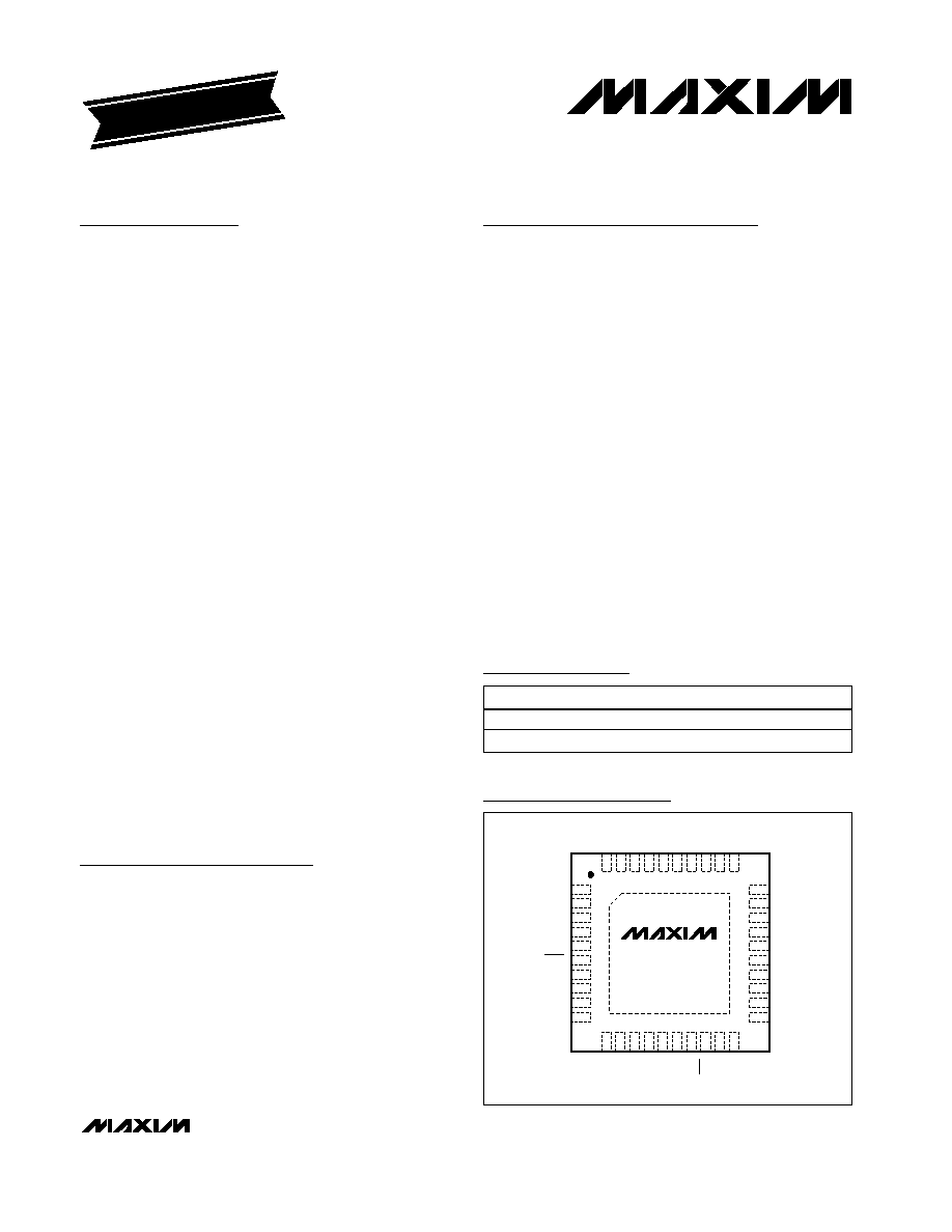
V
DD
DLM
LXM
BSTM
D1
D2
D3
VROK
D0
DHM
SUS
S0
S1
OFS
REF
ILIM
V
CC
TON
TIME
1
2
3
4
5
6
7
8
9
10
11
12
13
14
15
16
17
18
19
20
40
39
38
37
36
35
34
33
32
31
30
29
28
27
26
25
24
23
22
21
FB
OAIN-
OAIN+
CODE
D4
CCI
GNDS
CCV
GND
CSN
CMN
CMP
V+
BSTS
LXS
DHS
DLS
PGND
CSP
THIN QFN
MAX1519
MAX1545
TOP VIEW
SHDN
SKIP
Pin Configuration
Ordering Information
19-2734; Rev 1; 9/03
For pricing, delivery, and ordering information, please contact Maxim/Dallas Direct! at
1-888-629-4642, or visit Maxim's website at www.maxim-ic.com.
EVALUATION KIT
AVAILABLE
PART
TEMP RANGE
PIN-PACKAGE
MAX1519ETL
-40°C to +100°C
40 Thin QFN 6mm
6mm
MAX1545ETL
-40°C to +100°C
40 Thin QFN 6mm
6mm
Quick-PWM is a trademark of Maxim Integrated Products, Inc.
Pentium is a registered trademark of Intel Corp.
MAX1519/MAX1545
Dual-Phase, Quick-PWM Controllers for
Programmable CPU Core Power Supplies
2
_______________________________________________________________________________________
ABSOLUTE MAXIMUM RATINGS
Stresses beyond those listed under "Absolute Maximum Ratings" may cause permanent damage to the device. These are stress ratings only, and functional
operation of the device at these or any other conditions beyond those indicated in the operational sections of the specifications is not implied. Exposure to
absolute maximum rating conditions for extended periods may affect device reliability.
V+ to GND ..............................................................-0.3V to +30V
V
CC
to GND ..............................................................-0.3V to +6V
V
DD
to PGND............................................................-0.3V to +6V
SKIP, SUS, D0D4 to GND.......................................-0.3V to +6V
ILIM, FB, OFS, CCV, CCI, REF, OAIN+,
OAIN- to GND.........................................-0.3V to (V
CC
+ 0.3V)
CMP, CSP, CMN, CSN, GNDS to GND ......-0.3V to (V
CC
+ 0.3V)
TON, TIME, VROK, S0S1, CODE to GND.-0.3V to (V
CC
+ 0.3V)
SHDN to GND (Note 1)...........................................-0.3V to +18V
DLM, DLS to PGND ....................................-0.3V to (V
DD
+ 0.3V)
BSTM, BSTS to GND ..............................................-0.3V to +36V
DHM to LXM ...........................................-0.3V to (V
BSTM
+ 0.3V)
LXM to BSTM............................................................-6V to +0.3V
DHS to LXS..............................................-0.3V to (V
BSTS
+ 0.3V)
LXS to BSTS .............................................................-6V to +0.3V
GND to PGND .......................................................-0.3V to +0.3V
REF Short-Circuit Duration .........................................Continuous
Continuous Power Dissipation (T
A
= +70°C)
40-Pin 6mm
6mm Thin QFN
(derate 23.2mW/°C above +70°C) ...............................1.860W
Operating Temperature Range .........................-40°C to +100°C
Junction Temperature ......................................................+150°C
Storage Temperature Range .............................-65°C to +150°C
Lead Temperature (soldering, 10s) .................................+300°C
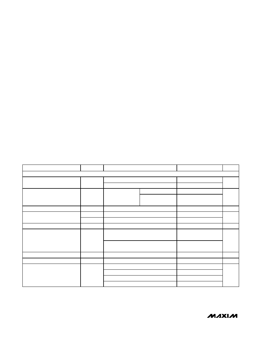
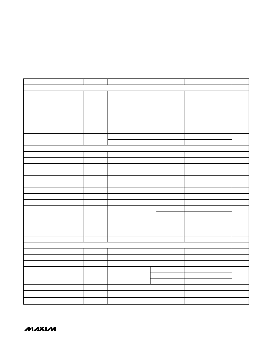
ELECTRICAL CHARACTERISTICS
(Circuit of Figure 1, V+ = 15V, V
CC
= V
DD
= V
SHDN
= V
TON
= V
SKIP
= V
S0
= V
S1
= V
CODE
= 5V, V
FB
= V
CMP
= V
CMN
= V
CSP
= V
CSN
= 1.3V, OFS = SUS = GNDS = D0D4 = GND; T
A
= 0°C to +85°C, unless otherwise specified. Typical values are at T
A
= +25°C.)
PARAMETER
SYMBOL
CONDITIONS
MIN
TYP
MAX
UNITS
PWM CONTROLLER
Battery voltage, V+
4
28
Input Voltage Range
V
CC
, V
DD
4.5
5.5
V
DAC codes
1V
-10
+10
DC Output Voltage Accuracy
(Note 2)
V+ = 4.5V to 28V,
includes load
regulation error
DAC codes from
0.60V to 1V
-15
+15
mV
Line Regulation Error
V
CC
= 4.5V to 5.5V, V+ = 4.5V to 28V
5
mV
I
FB
, I
GNDS
FB, GNDS
-2
+2
Input Bias Current
I
OFS
OFS
-0.1
+0.1
µA
OFS Input Range
0
2
V
V
OUT
/
V
OFS;
V
OFS
= V
OFS,
V
OFS
= 0 to 1V
-0.129
-0.125
-0.117
OFS Gain
A
OFS
V
OUT
/
V
OFS;
V
OFS
= V
OFS
- V
REF,
V
OFS
= 1V to 2V
-0.129
-0.125
-0.117
V/V
GNDS Input Range
-20
+200
mV
GNDS Gain
A
GNDS
V
OUT
/
V
GNDS
0.97
0.99
1.01
V/V
1000kHz nominal, R
TIME
= 15k
900
1000
1100
500kHz nominal, R
TIME
= 30k
460
500
540
250kHz nominal, R
TIME
= 60k
225
250
275
TIME Frequency Accuracy
f
TIME
Shutdown, R
TIME
= 30k
125
kHz
Note 1: SHDN may be forced to 12V for the purpose of debugging prototype boards using the no-fault test mode, which disables
fault protection and overlapping operation.
MAX1519/MAX1545
Dual-Phase, Quick-PWM Controllers for
Programmable CPU Core Power Supplies
_______________________________________________________________________________________
3
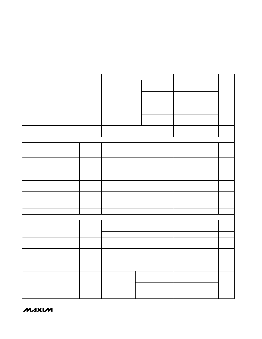
ELECTRICAL CHARACTERISTICS (continued)
(Circuit of Figure 1, V+ = 15V, V
CC
= V
DD
= V
SHDN
= V
TON
= V
SKIP
= V
S0
= V
S1
= V
CODE
= 5V, V
FB
= V
CMP
= V
CMN
= V
CSP
= V
CSN
= 1.3V, OFS = SUS = GNDS = D0D4 = GND; T
A
= 0°C to +85°C, unless otherwise specified. Typical values are at T
A
= +25°C.)
PARAMETER
SYMBOL
CONDITIONS
MIN
TYP
MAX
UNITS
TON = GND
(550kHz)
155
180
205
TON = REF
(300kHz)
320
355
390
TON = open
(200kHz)
475
525
575
On-Time (Note 3)
t
ON
V+ = 12V,
V
FB
= V
CCI
= 1.2V
TON = V
CC
(100kHz)
920
1000
1140
ns
TON = GND
300
375
Minimum Off-Time (Note 3)
t
OFF(MIN)
TON = V
CC
, open, or REF
400
480
ns
BIAS AND REFERENCE
Quiescent Supply Current (V
CC
)
I
CC
Measured at V
CC
, FB forced above the
regulation point, OAIN- = FB,
V
OAIN+
= 1.3V
1.70
3.20
mA
Quiescent Supply Current (V
DD
)
I
DD
Measured at V
DD
, FB forced above the
regulation point
<1
5
µA
Quiescent Battery Supply Current
(V+)
I
V+
Measured at V+
25
40
µA
Shutdown Supply Current (V
CC
)
Measured at V
CC
,
SHDN = GND
4
10
µA
Shutdown Supply Current (V
DD
)
Measured at V
DD
,
SHDN = GND
<1
5
µA
Shutdown Battery Supply Current
(V+)
Measured at V+,
SHDN = GND,
V
CC
= V
DD
= 0 or 5V
<1
5
µA
Reference Voltage
V
REF
V
CC
= 4.5V to 5.5V, I
REF
= 0
1.990
2.000
2.010
V
Reference Load Regulation
V
REF
I
REF
= -10µA to +100µA
-10
+10
mV
FAULT PROTECTION
SKIP = V
CC
, measured at FB with respect
to unloaded output voltage
13
16
19
%
Output Overvoltage Protection
Threshold (MAX1545 Only)
V
OVP
SKIP = REF or GND
2.00
V
Output Overvoltage Propagation
Delay (MAX1545 Only)
t
OVP
FB forced 2% above trip threshold
10
µs
Output Undervoltage Protection
Threshold
V
UVP
Measured at FB with respect to unloaded
output voltage
67
70
73
%
Output Undervoltage Propagation
Delay
t
UVP
FB forced 2% below trip threshold
10
µs
Lower threshold
(undervoltage)
-12
-10
-8
VROK Threshold
Measured at FB
with respect to
unloaded output
voltage
Upper threshold
(overvoltage)
SKIP = V
CC
+8
+10
+12
%
MAX1519/MAX1545
Dual-Phase, Quick-PWM Controllers for
Programmable CPU Core Power Supplies
4
_______________________________________________________________________________________
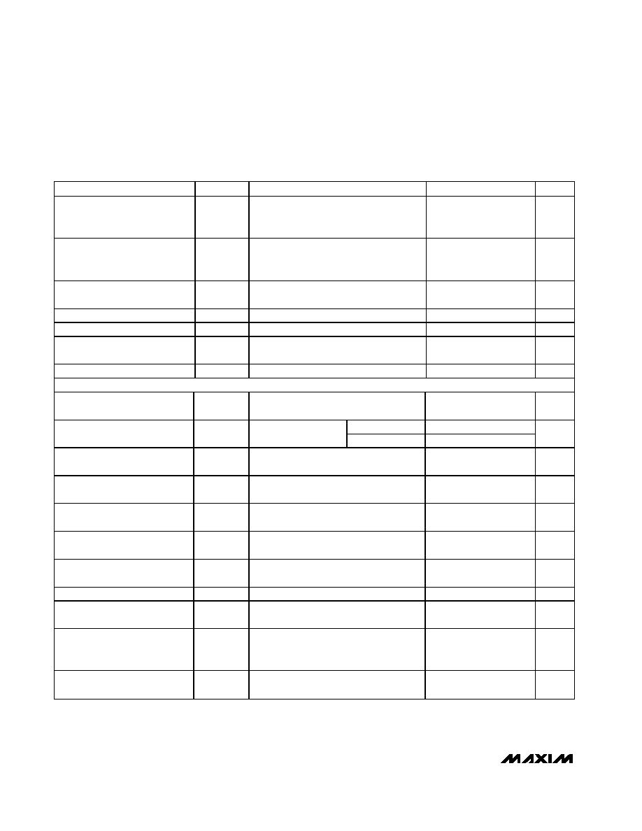
ELECTRICAL CHARACTERISTICS (continued)
(Circuit of Figure 1, V+ = 15V, V
CC
= V
DD
= V
SHDN
= V
TON
= V
SKIP
= V
S0
= V
S1
= V
CODE
= 5V, V
FB
= V
CMP
= V
CMN
= V
CSP
= V
CSN
= 1.3V, OFS = SUS = GNDS = D0D4 = GND; T
A
= 0°C to +85°C, unless otherwise specified. Typical values are at T
A
= +25°C.)
PARAMETER
SYMBOL
CONDITIONS
MIN
TYP
MAX
UNITS
Output Undervoltage Fault and
VROK Transition Blanking Time
(Note 4)
t
BLANK
Measured from the time when FB reaches
the voltage set by the DAC code; clock
speed set by R
TIME
24
Clks
VROK Startup Delay
Measured from the time when FB first
reaches the voltage set by the DAC code
after startup
3
5
7
ms
VROK Delay
t
VROK
FB forced 2% outside the VROK trip
threshold
10
µs
VROK Output Low Voltage
I
SINK
= 3mA
0.4
V
VROK Leakage Current
High state, VROK forced to 5.5V
1
µA
V
CC
Undervoltage Lockout
Threshold
V
UVLO(VCC)
Rising edge, hysteresis = 90mV, PWM
disabled below this level
4.0
4.25
4.4
V
Thermal-Shutdown Threshold
T
SHDN
Hysteresis = 10°C
160
°C
CURRENT LIMIT AND BALANCE
Current-Limit Threshold Voltage
(Positive, Default)
V
LIMIT
CMP - CMN, CSP - CSN; ILIM = V
CC
28
30
32
mV
V
ILIM
= 0.2V
8
10
12
Current-Limit Threshold Voltage
(Positive, Adjustable)
V
LIMIT
CMP - CMN,
CSP - CSN
V
ILIM
= 1.5V
73
75
77
mV
Current-Limit Threshold Voltage
(Negative)
V
LIMIT(NEG)
CMP - CMN, CSP - CSN; ILIM = V
CC
,
SKIP = V
CC
-41
-36
-31
mV
Current-Limit Threshold Voltage
(Zero Crossing)
V
ZERO
CMP - CMN, CSP - CSN;
SKIP = GND
1.5
mV
CMP, CMN, CSP, CSN Input
Ranges
0
2
V
CMP, CMN, CSP, CSN Input
Current
V
CSP
= V
CSN
= 0 to 5V
-2
+2
µA
Secondary Driver-Disable
Threshold
V
CSP
3
V
CC
- 1
V
CC
-
0.4
V
ILIM Input Current
I
ILIM
V
ILIM
= 0 to 5V
0.1
200
nA
Current-Limit Default Switchover
Threshold
V
ILIM
3
V
CC
- 1
V
CC
-
0.4
V
Current-Balance Offset
V
OS(IBAL)
(V
CMP
- V
CMN
) - (V
CSP
- V
CSN
); I
CCI
= 0,
-20mV < (V
CMP
- V
CMN
) < 20mV,
1.0V < V
CCI
< 2.0V
-2
+2
mV
Current-Balance
Transconductance
G
m(IBAL)
400
µS
MAX1519/MAX1545
Dual-Phase, Quick-PWM Controllers for
Programmable CPU Core Power Supplies
_______________________________________________________________________________________
5
ELECTRICAL CHARACTERISTICS (continued)
(Circuit of Figure 1, V+ = 15V, V
CC
= V
DD
= V
SHDN
= V
TON
= V
SKIP
= V
S0
= V
S1
= V
CODE
= 5V, V
FB
= V
CMP
= V
CMN
= V
CSP
= V
CSN
= 1.3V, OFS = SUS = GNDS = D0D4 = GND; T
A
= 0°C to +85°C, unless otherwise specified. Typical values are at T
A
= +25°C.)
PARAMETER
SYMBOL
CONDITIONS
MIN
TYP
MAX
UNITS
GATE DRIVERS
DH_ Gate-Driver On-Resistance
R
ON(DH)
BST_ - LX_ forced to 5V
1.0
4.5
High state (pullup)
1.0
4.5
DL_ Gate-Driver On-Resistance
R
ON(DL)
Low start (pulldown)
0.4
2
DH_ Gate-Driver Source/Sink
Current
I
DH
DH_ forced to 2.5V,
BST_ - LX_ forced to 5V
1.6
A
DL_ Gate-Driver Sink Current
I
DL(SINK)
DL_ forced to 5V
4
A
DL_ Gate-Driver Source Current
I
DL(SOURCE)
DL_ forced to 2.5V
1.6
A
DL_ rising
35
Dead Time
t
DEAD
DH_ rising
26
ns
VOLTAGE-POSITIONING AMPLIFIER
Input Offset Voltage
V
OS
-1
+1
mV
Input Bias Current
I
BIAS
OAIN+, OAIN-
0.1
200
nA
Op Amp Disable Threshold
V
OAIN-
3
V
CC
- 1
V
CC
-
0.4
V
Common-Mode Input Voltage
Range
V
CM
Guaranteed by CMRR test
0
2.5
V
Common-Mode Rejection Ratio
CMRR
V
OAIN+
= V
OAIN-
= 0 to 2.5V
70
115
dB
Power-Supply Rejection Ratio
PSRR
V
CC
= 4.5V to 5.5V
75
100
dB
Large-Signal Voltage Gain
A
OA
R
L
= 1k
to V
CC
/2
80
112
dB
V
CC
- V
FBH
77
300
Output Voltage Swing
|V
OAIN+
- V
OAIN-
|
10mV,
R
L
= 1k
to V
CC
/2
V
FBL
47
200
mV
Input Capacitance
11
pF
Gain-Bandwidth Product
3
MHz
Slew Rate
0.3
V/µs
Capacitive-Load Stability
No sustained oscillations
400
pF
LOGIC AND I/O
SHDN Input High Voltage
V
IH
0.8
V
SHDN Input Low Voltage
V
IL
0.4
V
SHDN No-Fault Threshold
V
SHDN
12
15
V
High
2.7
REF
1.2
2.3
Three-Level Input Logic Levels
SUS,
SKIP
Low
0.8
V
Logic Input Current
SHDN, SUS, SKIP
-1
+1
µA
D0D4 Logic Input High Voltage
1.6
V
D0D4 Logic Input Low Voltage
0.8
V