Äîêóìåíòàöèÿ è îïèñàíèÿ www.docs.chipfind.ru
General Description
The MAX1540/MAX1541 dual pulse-width modulation
(PWM) controllers provide the high efficiency, excellent
transient response, and high DC-output accuracy nec-
essary for stepping down high-voltage batteries to gen-
erate low-voltage chipset and RAM power supplies in
notebook computers.
The Maxim proprietary Quick-PWMTM controllers are
free running, constant on-time with input feed forward.
This configuration provides ultra-fast transient
response, wide input-output (I/O) differential range, low
supply current, and tight load-regulation characteris-
tics. The controllers can accurately sense the inductor
current across an external current-sense resistor in
series with the output to ensure reliable overload and
inductor saturation protection. Alternatively, the con-
trollers can use the synchronous rectifier itself or loss-
less inductor current-sensing methods to provide
overload protection with lower power dissipation.
For a single step-down PWM controller with inductor-
saturation protection, external-reference input voltage,
and dynamically selectable output voltages, refer to the
MAX1992/MAX1993 data sheet.
Applications
Notebook Computers
Core/IO Supplies as Low as 0.7V
0.7V to 5.5V Supply Rails
CPU/Chipset/GPU with Dynamic Voltage Core
Supplies (MAX1541)
DDR Memory Termination (MAX1541)
Active Termination Buses (MAX1541)
Features
Inductor-Saturation Protection
Accurate Differential Current-Sense Inputs
Dual Ultra-High-Efficiency Quick-PWMs with
100ns Load-Step Response
MAX1540
1.8V/1.2V Fixed or 0.7V to 5.5V Adjustable
Output (OUT1)
2.5V/1.5V Fixed or 0.7V to 5.5V Adjustable
Output (OUT2)
Fixed 5V, 100mA Linear Regulator
MAX1541
External Reference Input (REFIN1)
Dynamically Selectable Output Voltage--0.7V
to 5.5V (OUT1)
2.5V/1.8V Fixed or 0.7V to 5.5V Adjustable
Output (OUT2)
Optional Power-Good and Fault Blanking
During Transitions
Fixed 5V or Adjustable 100mA Linear Regulator
1% V
OUT
Accuracy over Line and Load
2V to 28V Battery Input Range
170kHz to 620kHz Selectable Switching
Frequency
Overvoltage/Undervoltage-Protection Option
1.7ms Digital Soft-Start
Drives Large Synchronous-Rectifier FETs
2V ±0.7% Reference Output
Separate Power-Good Window Comparators
MAX1540/MAX1541
Dual Step-Down Controllers with Saturation
Protection, Dynamic Output, and Linear Regulator
________________________________________________________________ Maxim Integrated Products
1
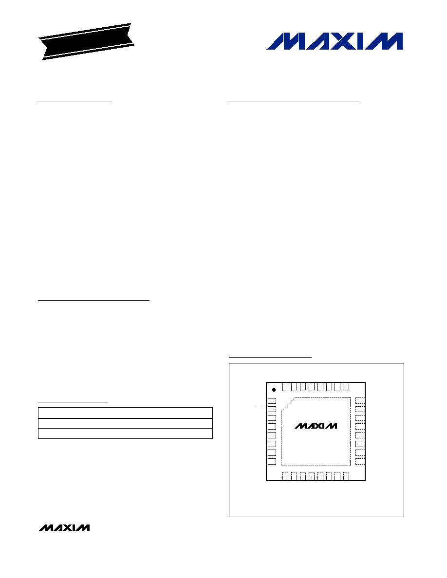
THIN QFN
TOP VIEW
32
31
30
29
28
27
26
ON1
ON2
CSP1
CSN1
FB1
OUT1
PGOOD1
25
DH1
9
10
11
12
13
14
15
CSP2
CSN2
FB2
OUT2
PGOOD2
DH2
LX2
16
BST2
17
18
19
20
21
22
23
GND
DL2
V+
LDOOUT
DL1
LDOON
BST1
8
7
6
5
4
3
2
REF
ILIM2
ILIM1
V
CC
TON
LSAT
SKIP
MAX1540
1
OVP/UVP
24
LX1
Pin Configurations
19-2861; Rev 2; 1/05
For pricing, delivery, and ordering information, please contact Maxim/Dallas Direct! at
1-888-629-4642, or visit Maxim's website at www.maxim-ic.com.
EVALUATION KIT
AVAILABLE
Quick-PWM is a trademark of Maxim Integrated Products, Inc.
Ordering Information
PART
TEMP RANGE
PIN-PACKAGE
MAX1540ETJ
-40
°C to +85°C 32 Thin QFN 5mm x 5mm
MAX1541ETL
-40
°C to +85°C 40 Thin QFN 6mm x 6mm
Pin Configurations continued at end of data sheet.
MAX1540/MAX1541
Dual Step-Down Controllers with Saturation
Protection, Dynamic Output, and Linear Regulator
2
_______________________________________________________________________________________
ABSOLUTE MAXIMUM RATINGS
Stresses beyond those listed under "Absolute Maximum Ratings" may cause permanent damage to the device. These are stress ratings only, and functional
operation of the device at these or any other conditions beyond those indicated in the operational sections of the specifications is not implied. Exposure to
absolute maximum rating conditions for extended periods may affect device reliability.
Note 1: For the MAX1540, the gate-driver input supply (V
DD
) is internally connected to the fixed 5V linear-regulator output (LDOOUT),
and the linear-regulator input supply (LDOIN) is internally connected to the battery voltage input (V+).
V+, LDOON to GND ...............................................-0.3V to +28V
LDOOUT to GND (MAX1540, Note 1) ......................-0.3V to +6V
LDOOUT to GND (MAX1541, Note 1) ....................-0.3V to +28V
V
DD
to GND (MAX1541, Note 1) ..............................-0.3V to +6V
V
CC
, ON_ to GND.....................................................-0.3V to +6V
SKIP, PGOOD_ to GND............................................-0.3V to +6V
FB_, CSP_, ILIM_ to GND.........................................-0.3V to +6V
TON, OVP/UVP, LSAT to GND ...................-0.3V to (V
CC
+ 0.3V)
REF, OUT_ to GND.....................................-0.3V to (V
CC
+ 0.3V)
LDOIN to GND (MAX1541).....................................-0.3V to +28V
REFIN1, GATE, OD, FBLDO to GND (MAX1541).....-0.3V to +6V
FBLANK, CC1 to GND (MAX1541).............-0.3V to (V
CC
+ 0.3V)
DL_ to GND (Note 1) ..................................-0.3V to (V
DD
+ 0.3V)
CSN_ to GND ............................................................-2V to +30V
DH_ to LX_..................................................-0.3V to (BST + 0.3V)
LX_ to GND................................................................-2V to +30V
BST_ to LX_ ..............................................................-0.3V to +6V
REF Short Circuit to GND ...........................................Continuous
Continuous Power Dissipation (T
A
= +70
°C)
32-Pin 5mm x 5mm Thin QFN (derated 21.3mW/
°C
above +70
°C).............................................................1702mW
40-Pin 6mm x 6mm Thin QFN (derated 26.3mW/
°C
above +70
°C).............................................................2105mW
Operating Temperature Range
MAX154_ET_ ...................................................-40°C to +85°C
Junction Temperature ......................................................+150°C
Storage Temperature Range .............................-65°C to +150°C
Lead Temperature (soldering, 10s) .................................+300°C
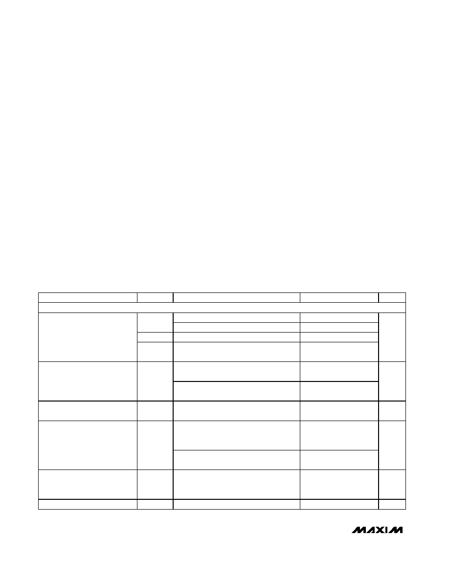
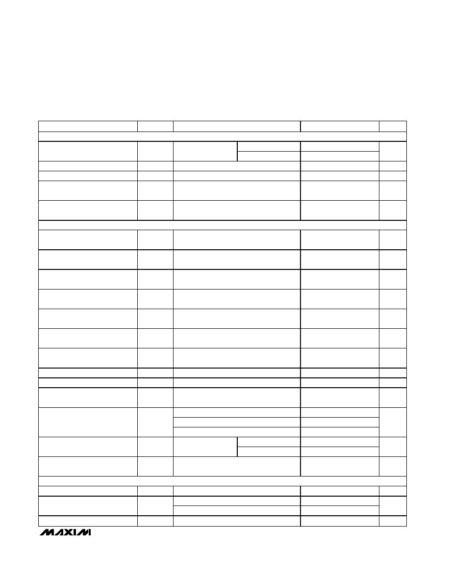
ELECTRICAL CHARACTERISTICS
(V+ = 15V, V
CC
= V
DD
= ON1 = ON2 = 5V, SKIP = GND, LDOIN (MAX1541) = V+, T
A
= 0°C to +85°C, unless otherwise noted. Typical
values are at T
A
= +25
°C.)
PARAMETER
SYMBOL
CONDITIONS
MIN
TYP
MAX
UNITS
INPUT SUPPLIES (Note 1)
MAX1540: battery voltage, V+ > V
LDOOUT
5.5
28
V
IN
MAX1541: battery voltage, V+ > V
LDOOUT
2
28
V
BIAS
V
CC,
V
DD
(MAX1541)
4.5
5.5
Input Voltage Range
V
LDOIN
MAX1541: LDO input supply,
V
LDOIN
> V
LDOOUT
4.5
28
V
FB1 and FB2 forced above the regulation
point, LSAT = GND
0.7
1.5
Quiescent Supply Current (V
CC
)
I
CC
FB1 and FB2 forced above the regulation
point, ON1 or ON2 = V
CC
, V
LSAT
> 0.5V
1.8
mA
Quiescent Supply Current
(V
DD
, MAX1541 Only)
I
DD
FB1 and FB2 forced above the regulation
point, ON1 or ON2 = V
CC
<1
5
µA
MAX1540: FB1 and FB2 forced above the
regulation point, ON1 or ON2 = V
CC
,
V
LDOON
= V+ = 28V
150
Quiescent Supply Current (V+)
I
V+
MAX1541: ON1 or ON2 = V
CC
,
V
LDOON
= V+ = 28V
25
40
µA
Quiescent Supply Current
(LDOIN, MAX1541 Only)
I
LDOIN
FB1 and FB2 forced above the regulation
point, ON1 or ON2 = V
CC
,
V
LDOON
= V+ = 28V
110
µA
Standby Supply Current (V
CC
)
ON1 = ON2 = GND, V
LDOON
= V+ = 28V
<1
5
µA
MAX1540/MAX1541
Dual Step-Down Controllers with Saturation
Protection, Dynamic Output, and Linear Regulator
_______________________________________________________________________________________
3
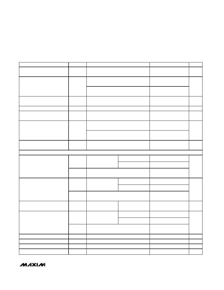
ELECTRICAL CHARACTERISTICS (continued)
(V+ = 15V, V
CC
= V
DD
= ON1 = ON2 = 5V, SKIP = GND, LDOIN (MAX1541) = V+, T
A
= 0°C to +85°C, unless otherwise noted. Typical
values are at T
A
= +25
°C.)
PARAMETER
SYMBOL
CONDITIONS
MIN
TYP
MAX
UNITS
Standby Supply Current
(V
DD
, MAX1541 Only)
ON1 = ON2 = GND, V
LDOON
= V+ = 28V
<1
5
µA
MAX1540: ON1 = ON2 = GND,
LDOON = V+ = 28V, V
CC
= 0 or 5V
105
Standby Supply Current (V+)
MAX1541: ON1 = ON2 = GND,
LDOON = V+ = 28V, V
CC
= V
DD
= 0 or 5V
<1
5
µA
Standby Supply Current
(LDOIN, MAX1541 Only)
ON1 = ON2 = GND, V
LDOON
= V+ = 28V
100
µA
Shutdown Supply Current (V
CC
)
ON1 = ON2 = LDOON = GND
<1
5
µA
Shutdown Supply Current
(V
DD
, MAX1541 Only)
ON1 = ON2 = LDOON = GND
<1
5
µA
MAX1540: ON1 = ON2 = LDOON = GND,
V+ = 28V, V
CC
= 0 or 5V
4
15
Shutdown Supply Current (V+)
MAX1541: ON1 = ON2 = LDOON = GND,
V+ = 28V, V
CC
= V
DD
= 0 or 5V
<1
5
µA
Shutdown Supply Current
(LDOIN, MAX1541 Only)
LDOON = GND
4
10
µA
PWM CONTROLLERS
FB1 = GND
1.782
1.80
1.818
V
OUT1
Preset output,
V+ = 5.5V to 28V,
SKIP = V
CC
FB1 = V
CC
1.188
1.20
1.212
MAX1540 Main Output-Voltage
Accuracy (OUT1) (Note
2)
V
FB1
Adjustable output, V+ = 5.5V to 28V,
SKIP = V
CC
0.693
0.70
0.707
V
FB2 = GND
2.475
2.50
2.525
V
OUT2
Preset output,
V+ = 5.5V to 28V,
SKIP = V
CC
FB2 = V
CC
1.485
1.50
1.515
MAX1540 Secondary Output-
Voltage Accuracy (OUT2)
(Note 2)
V
FB2
Adjustable output, V+ = 5.5V to 28V,
SKIP = V
CC
0.693
0.70
0.707
V
MAX1541 Main Feedback-
Voltage Accuracy (FB1)
V
FB1
V+ = 4.5V to 28V,
SKIP = V
CC
REFIN1 = 0.35 x REF
0.693
0.70
0.707
V
FB2 = GND
2.475
2.50
2.525
V
OUT2
Preset output,
V+ = 4.5V to 28V,
SKIP = V
CC
FB2 = V
CC
1.782
1.80
1.818
MAX1541 Secondary Output-
Voltage Accuracy (OUT2)
(Note 2)
V
FB2
Adjustable output, V+ = 4.5V to 28V,
SKIP = V
CC
0.693
0.70
0.707
V
Load-Regulation Error
I
LOAD
= 0 to 3A, SKIP = V
CC
0.1
%
Line-Regulation Error
V
CC
= 4.5V to 5.5V, V+ = 4.5V to 28V
0.25
%
FB_ Input Bias Current
I
FB
_
-0.1
+0.1
µA
Output Adjust Range
0.7
5.5
V
MAX1540/MAX1541
Dual Step-Down Controllers with Saturation
Protection, Dynamic Output, and Linear Regulator
4
_______________________________________________________________________________________
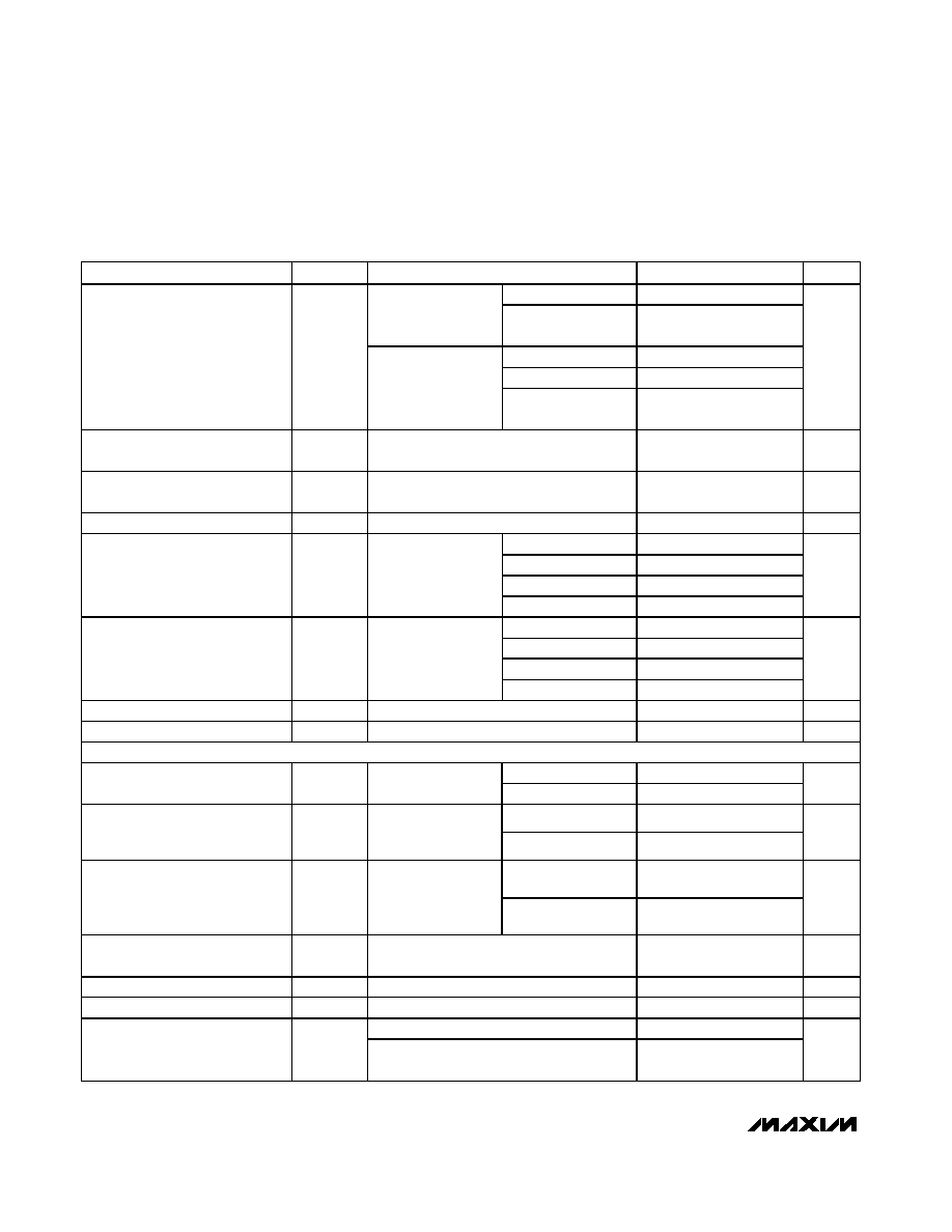
ELECTRICAL CHARACTERISTICS (continued)
(V+ = 15V, V
CC
= V
DD
= ON1 = ON2 = 5V, SKIP = GND, LDOIN (MAX1541) = V+, T
A
= 0°C to +85°C, unless otherwise noted. Typical
values are at T
A
= +25
°C.)
PARAMETER
SYMBOL
CONDITIONS
MIN
TYP
MAX
UNITS
FB_ = GND
70
145
350
MAX1540
FB_ = V
CC
or
adjustable
50
115
220
FB1 = OUT1
400
700
1500
FB2 = GND
90
170
350
OUT_ Input Resistance
R
OUT
_
MAX1541
FB2 = V
CC
or
adjustable
60
130
270
k
OUT_ Discharge Mode On-
Resistance
R
D IS C H ARGE
10
25
OUT_ Synchronous-Rectifier
Discharge-Mode Turn-On Level
0.2
0.3
0.4
V
Soft-Start Ramp Time
t
SS
Rising edge on ON_ to full current limit
1.7
ms
TON = GN D ( 620kH z)
149
169
190
TON = REF (485kHz)
191
216
242
TON = op en ( 345kH z) 274
304
335
DH1 On-Time
t
ON1
V+ = 15V,
V
OUT1
= 1.5V
(Note 3)
TON = V
CC
(235kHz)
402
447
491
ns
TON = GN D ( 460kH z) 201
228
256
TON = REF (355kHz)
260
296
331
TON = op en ( 255kH z) 371
412
453
DH2 On-Time
t
ON2
V+ = 15V,
V
OUT2
= 1.5V
(Note 3)
TON = V
CC
(170kHz)
556
618
679
ns
On-Time Tracking
t
ON2
with respect to t
ON1
(Note 3)
120
135
150
%
Minimum Off-Time
t
OFF(MIN)
(Note 3)
400
500
ns
LINEAR REGULATOR (LDO) (Note 1)
0 < I
LDOOUT
< 10mA
4.85
5.0
5.10
MAX1540 LDO Output-Voltage
Accuracy
V
LDOOUT
ON1 = ON2 = GND,
V+ = 6V to 28V
0 < I
LD OOU T
< 100m A
4.70
5.10
V
0 < I
LDOOUT
< 10mA
4.85
5.0
5.10
MAX1541 LDO Output-Voltage
Accuracy (Fixed V
LDOOUT
)
V
LDOOUT
FBLDO = ON1 =
ON2 = GND,
V
LDOIN
= 6V to 28V
0 < I
LD OOU T
< 100m A
4.70
5.10
V
0 < I
LDOOUT
< 10mA
1.212
1.25
1.275
MAX1541 LDO Feedback
Accuracy (Adjustable V
LDOOUT
)
V
FBLDO
FBLDO = LDOOUT,
ON1 = ON2 = GND,
V
LDOIN
= 4.5V to
28V
0 < I
LD OOU T
< 100m A
1.175
1.275
V
MAX1541 LDO Output
Adjust Range
1.175
24
V
LDOOUT Short-Circuit Current
130
mA
FBLDO Input Bias Current
I
FBLDO
-0.1
+0.1
µA
MAX1540: V+ - V
LDOOUT
, I
LDOOUT
= 50mA
500
800
Dropout Voltage
MAX1541: V
LDOIN
- V
LDOOUT
,
I
LDOOUT
= 50mA
500
800
mV
MAX1540/MAX1541
Dual Step-Down Controllers with Saturation
Protection, Dynamic Output, and Linear Regulator
_______________________________________________________________________________________
5
ELECTRICAL CHARACTERISTICS (continued)
(V+ = 15V, V
CC
= V
DD
= ON1 = ON2 = 5V, SKIP = GND, LDOIN (MAX1541) = V+, T
A
= 0°C to +85°C, unless otherwise noted. Typical
values are at T
A
= +25
°C.)
PARAMETER
SYMBOL
CONDITIONS
MIN
TYP
MAX
UNITS
REFERENCE (REF)
T
A
= + 25° C to + 85
° C 1.986
2.00
2.014
Reference Voltage
V
REF
V
CC
= 4.5V to 5.5V,
I
REF
= 0V
T
A
= 0° C to +85°C
1.983
2.00
2.017
V
Reference Load Regulation
V
REF
I
REF
= -10µA to +50µA
-0.01
+0.01
V
REF Lockout Voltage
V
REF(UVLO)
Rising edge, hysteresis = 350mV
1.95
V
REFIN1 (MAX1541)
Voltage Range
V
REFIN
0.7
V
REF
V
REFIN1 (MAX1541)
Input Bias Current
I
REFIN1
0.01
0.05
µA
FAULT DETECTION
Overvoltage Trip Threshold
With respect to error-comparator threshold,
OVP/UVP = V
CC
12
16
20
%
Overvoltage Fault-Propagation
Delay
t
OVP
FB forced 2% above trip threshold
10
µs
Output Undervoltage-Protection
Trip Threshold
With respect to error-comparator threshold,
OVP/UVP = V
CC
65
70
75
%
Output Undervoltage-Protection
Blanking Time
t
BLANK
From rising edge of ON_
10
35
ms
Output Undervoltage Fault-
Propagation Delay
t
UVP
10
µs
PGOOD_ Lower Trip Threshold
With respect to error-comparator threshold,
hysteresis = 1%
-13
-10
-7
%
PGOOD_ Upper Trip Threshold
With respect to error-comparator threshold,
hysteresis = 1%
+7
+10
+13
%
PGOOD_ Propagation Delay
t
PGOOD
_
FB forced 2% beyond P GOOD _ trip threshold
10
µs
PGOOD_ Output Low Voltage
I
SINK
= 4mA
0.3
V
PGOOD_ Leakage Current
I
PGOOD
_
FB = REF (PGOOD high impedance),
PGOOD forced to 5.5V
1
µA
FBLANK = V
CC
120
220
320
FBLANK = open
80
140
205
Fault-Blanking Time
(MAX1541 Only)
t
FBLANK
FBLANK = REF
35
65
95
µs
LDOON = V
CC
+150
Thermal-Shutdown Threshold
T
SHDN
Hysteresis = 10°C
LDOON = GND
+160
°C
V
CC
Undervoltage-Lockout
Threshold
V
UVLO(VCC)
Rising edge, PWM disabled below this
level, hysteresis = 20mV
4.1
4.25
4.4
V
CURRENT LIMIT
ILIM_ Adjustment Range
0.25
2
V
CSP_
0
2.7
Current-Limit Input Range
CSN_
-0.3
+28
V
CSP_/CSN_ Input Current
0.5
µA