_______________General Description
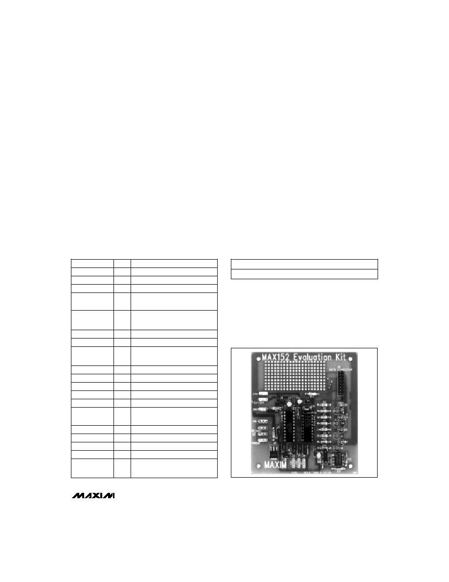
The MAX152 evaluation kit (EV kit) is fully assembled, and
provides a proven design and PC board layout for fast,
easy evaluation of the MAX152 at sample rates to
400ksps. An oscillator continuously triggers the converter,
and an LED displays the conversion results. Several
jumpers allow the board to be configured for the various
operating modes of the MAX152, and the board includes
the low-current shutdown circuit shown in the data sheet.
A 16-pin data connector provides easy interface between
the MAX152 EV kit and the user's system.
The MAX152 EV kit can be used to evaluate the 5V
MAX153 at sample rates to 1Msps.
____________________Component List
____________________________Features
o
High-Speed 8-Bit ADC
o
Unipolar or Bipolar Input
o
No Clock Circuit Required
o
+3V (MAX152) or +5V (MAX153) Operation
o
Low-Power Shutdown Mode
o
LED Display of Conversion Results
o
3in2 Prototyping Area
o
16-Pin Data Connector for Interface to
External System
______________Ordering Information
MAX152 EV Kit
MAX152 Evaluation Kit
________________________________________________________________________________________ 13
PART
TEMP. RANGE
BOARD TYPE
MAX152EVKIT-DIP
0°C to +70°C
Through-Hole
DESIGNATION
QTY
DESCRIPTION
U1
1
MAX152CPP
1
74HCT574
U3
1
ICM7555CPA
5
0.1µF ceramic capacitors
C2, C4
2
C5
1
100pF ceramic capacitor
D1-D8
8
Red LEDs
Q1
1
R1
1
300
5% resistor
R2, R12
2
510k
5% resistors
R3-R10
8
620
5% resistors
R11
1
10k
5% resistor
J1, J3
2
3-pin jumper headers
6
2-pin jumper headers
None
8
Shunts
None
1
16-pin ribbon cable connector
None
1
3.50" x 4.00" PC board
None
4
Rubber feet
None
1
U2
The MAX152EVKIT may also be used to evaluate the
MAX153. To receive a free sample of the
MAX153CPP, call 1-800-998-8800.
______________________________EV Kit
C1, C3, C6, C7,
C8
10µF 16V radial electrolytic
capacitors
ME12N06EL Nihon N-channel
logic-level MOSFET
J2, J4, J5, J6,
J7, J8
MAX152 data sheet and
EV kit manual

MAX152 EV Kit
___________________Quick Reference
The evaluation kit as shipped, is configured for the continuous-
conversion mode. To verify operation, follow these steps:
1. Verify that the jumpers are configured as
described in Table 2.
2. Connect the power supplies (+3V for MAX152,
+5V for MAX153) to the power input connector.
3. Connect an analog input to AIN input.
4. Read conversion results displayed on the LEDs.
_______________General Description
Jumper Functions
The MAX152 EV kit has several jumpers to alter the
configuration. Table 1 lists the jumpers and their func-
tions. Table 2 gives the jumper selection for a free-run-
ning mode used for board verification.
Note that Table 2's configuration drives both the
RD and
CS inputs and sets the MODE pin low. The timing dia-
gram for this configuration is shown in the MAX152 or
MAX153 data sheet. Refer to the data sheet for more
information on the various operating modes.
Power Requirements
The MAX152 EV kit may be used with either the
MAX152 or MAX153. The MAX152 will operate on sup-
plies as low as 2.7V. The MAX153 operates on +5V or
±5V. The positive supply is also connected to the octal
latch and ICM7555 timer on the board. The LEDs will
cause the positive supply current to approach 60mA
when all are on. The V
SS
input is connected only to the
MAX152/MAX153's V
SS
pin. The V
SS
pin will draw less
than 50µA. Optionally, J4 can be shorted to connect
V
SS
to ground when not using a negative supply.
MAX152/MAX153 Reference Voltage
The VREF+ and VREF- pins may be connected to any
potential between V
DD
and V
SS
. For single-supply
operation, VREF+ can be connected to V
DD
and VREF-
can be connected to ground. Jumpers (J1 and J2) are
provided for this configuration. If a reference voltage
other than V
DD
or ground is desired, connect the
source to the VREF+ and/or VREF- pads and set J1 and
J2 accordingly. Refer to Table 1 for their use.
MAX152/MAX153 Data Output/Display
The MAX152/MAX153's output is latched and buffered
by a 74HCT574 so it can drive an LED display. The
MAX152 Evaluation Kit
14
______________________________________________________________________________________
Table 2. Jumper Selection for Free-Running Mode
JUMPER CONNECTION
FUNCTION
J1
2 & 3
VREF- connected to GND
J2
Short
VREF+ connected to V
DD
J3
2 & 3
CS driven by ICM7555
J4
Short
V
SS
connected to GND. Leave
J4 open if a V
SS
source is used.
J5
Open
MODE pin internally pulled low
J6
Short
Enable the ICM7555
J7
Short
Enable the LED display
J8
Short
RD driven by ICM7555
Table 1. Jumper Functions
JUMPER CONNECTION
FUNCTION
MODE pin connected to V
DD
1 & 2
VREF- connected to the drain
of Q1
J2
Short
VREF+ shorted to V
DD
J3
Open
Used when an external digital
signal is applied to the
CS input
J4
Short
V
SS
connected to ground
J5
Open
MODE pin open (internally pulled
low)
J6
Open
ICM7555 circuit disabled
J7
Open
LED display disabled
J8
Open
Used when an external digital
input is applied to the
RD input
J1
Open
Used when connecting a voltage
source to the VREF- pad
Short
2 & 3
VREF- connected to ground
ICM7555 circuit enabled
Open
Used when connecting a voltage
source to the VREF+ pad
Short
1 & 2
CS grounded
Short
2 & 3
CS driven by the ICM7555
LED display enabled
Open
Used when driving V
SS
with a
negative source (-5V or -3V)
Short
RD driven by the ICM7555

LEDs display the output of the MAX152/MAX153 after
each conversion. Removing the J7 shunt will disable
the LED display and lower the positive supply current.
The clock signal for the 74HCT574 is taken off the
RD
input. This latches the MAX152/MAX153 conversion
results on the trailing (positive going) edge of the
RD
signal. This technique works as long as
RD pulse is
longer than the conversion time of the
MAX152/MAX153.
The ready (RDY) signal can be observed by configur-
ring the board per Table 2 and inserting a 4.7k
pull-
up resistor in the location marked R13. The RDY signal
will appear on the
WR/RDY pin. The resistor is normally
not installed, in order to keep the pin input current as
low as possible.
ICM7555 Circuit
A simple ICM7555 timer circuit on the board provides a
clock for the stand-alone mode. The output can be
connected to the
CS and RD pins through J3 and J8. It
will then trigger a conversion approximately every 2.5µs
when J6 is shorted. J6 is provided to disable the
ICM7555 when evaluating the shutdown currents.
When using external signal sources for
CS and RD,
leave jumpers J3 and J8 open. Refer to the data sheet
for timing specifications with external sources.
Shutdown Modes
The function of the power-down pin (
PWRDN) is to drop
the MAX152/MAX153's supply current to typically 1µA.
Note, however, that VREF+ will continue to appear to
the source as a 2k
resistor, and this resistor draws
current even when the device is in power-down mode.
The addition of MOSFET Q1 opens VREF- to discon-
nect this internal reference resistor and remove its cur-
rent drain. A 510k
resistor acts as the pull-up for the
gate of Q1 and
PWRDN. You can evaluate the power-
down mode simply by grounding the PWRDN pad.
The other chips on the board will continue to draw cur-
rent if they are left enabled. Be sure to disable the LED
display and the ICM7555 circuits for a true measure-
ment.
With the device and LEDs enabled, the supply current
may be 60mA. The current drops to less than 15mA
with the LEDs disabled. Using
PWRDN with VREF- con-
nected to ground will reduce the current to about
3.5mA. Finally, in power-down mode with VREF- dis-
abled by Q1 and the ICM7555 disabled, the supply
current will typically be less than 50µA. The actual
reading will include the MAX152/MAC153 V
DD
current,
static current for the 74HCT574, and 10µA drawn
through the 510k
resistor R2.
MAX152 EV Kit
MAX152 Evaluation Kit
______________________________________________________________________________________
15
MAX152 EV Kit
MAX152 Evaluation Kit
16
______________________________________________________________________________________
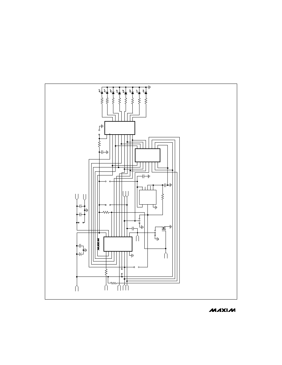
Figure 1. MAX152 EV Kit Schematic
D1
D3
D5
D7
2
4
6
8
+
2
Q0
Q1
Q2
Q3
Q4
Q6
Q7
19
18
17
16
15
14
13
12
+
V
IN
R13
OPEN
WR
/RDY
R1
300
J5
V
DD
RD
INT
J8
VREF-
1
2
3
4 5
6
7
8
9
10
20
19
18
17 16
15
14
13
12 11
V
IN
D0
D1
D2 D3
WR
/RDY
MODE
RD INT GND
V
DD V SS
PWRDN
D7 D6
D5
D4
CS
VREF+
VREF-
MAX152
U1
R2
510k
J2
J6
CS VREF+
ICM7555
U3
O
V+
GND
RS
CV
THR
DIS
TR
4
5
6
7
2
8
3
1
R11
10k
C5
100pF
C7
0.1µF
J1
J1
3
1
1
C8
O.1F
D1
D2
D3
D4
D5
D6
D7
D8
R3 620
R4 620
R5 620
R6 620
R7 620
R8 620
R9 620
R10 620
Q5
D0
D1
D2
D3
D4
D6
D7
D5
2
3
4
5
6
7
8
9
CLK
CE
74HCT574
U2
J7
R12
510k
DATA CONNECTOR
WR
/RD
RD
V
DD
GND
10
12
14
16
1
3
5
7
9
11
13
15
D0
D2
D4
D6
CS
INT
V
DD
GND
C2
22µF
V
SS
C1
0.1µF
GND
C3
0.1µF
C4
22µF
Q1
1
2
3
PWRDN
J4
J3
2
3
1
0.1µF
MAX152 EV Kit
MAX152 Evaluation Kit
______________________________________________________________________________________
17
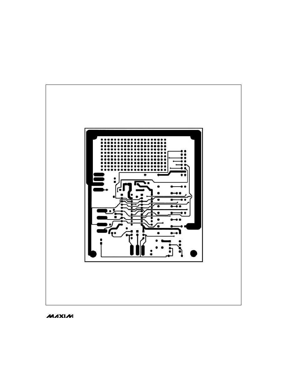
Figure 2. MAX152 EV Kit Component-Side Layout