General Description
The MAX1522 evaluation kit (EV kit) is a fully assembled
and tested surface-mount circuit board that contains
two separate step-up switching controller circuits. The
first circuit (left side) utilizes the MAX1524, is config-
ured for +5V output, and can deliver up to 1A of cur-
rent. The MAX1524 supply pin is bootstrapped to the
output. The second circuit (right side) utilizes the
MAX1522, is configured for +12V output, and can deliv-
er up to 200mA of current with the input voltage as low
as +2.7V.
The MAX1522 and MAX1524 feature soft-start and fault-
detect. The EV kit allows the user to set the on-time of
the N-channel MOSFETs to either 0.5µs or 3µs.
Features
o Input Voltage
+1.5V to +5.5V (Left Side, BOOTSTRAPPED)
+2.5V to +5.5V (Right Side, NON-
BOOTSTRAPPED)
o Output Voltage
+5V Output Up to 1A (Left Side)
+12V Output Up to 200mA (Right Side)
o No Current-Sense Resistor
o Fault-Detection
o Soft-Start Limits Inrush Current
o Selectable Maximum Duty Cycle (45% or 80%)
o Adjustable Output Voltages
o 1µA (max) Shutdown Current
o Switching Frequency Up to 1MHz
o Fully Assembled and Tested
Evaluates: MAX1522/MAX1523/MAX1524
MAX1522 Evaluation Kit
________________________________________________________________ Maxim Integrated Products
1
19-1974; Rev 0; 03/01
Ordering Information
Note: Please indicate that you are using the MAX1522,
MAX1523, or MAX1524 when contacting these component
suppliers.
Component Suppliers
SUPPLIER
PHONE
FAX
Fairchild
408-822-2000
408-822-2102
Murata
814-237-1431
814-238-0490
Nihon USA
661-867-2555
661-867-2698
Sanyo
619-661-6835
619-661-1055
Sumida
847-956-0666
847-956-0702
Taiyo Yuden
408-573-4150
408-573-4159
TDK
847-803-6100
847-803-6296
Toshiba
949-455-2000
949-859-3963
DESIGNATION
QTY
DESCRIPTION
C1, C2
2
100pF, 50V COG ceramic
capacitors (0603)
TDK C1608COG1H101JT or
Murata GRM39COG101J050AD
C3
1
47pF, 50V COG ceramic
capacitor (0603)
TDK C1608COG1H470JT
C4
1
330pF, 50V COG ceramic
capacitor (0603)
TDK C1608X7R1H331KT or
Murata GRM39COG331J050AD
C5
1
1µF, 16V X7R ceramic capacitor
(1206)
Taiyo Yuden EMK316BJ105KF or
TDK C3216X7R1C105KT
Component List
DESIGNATION
QTY
DESCRIPTION
C6, C7
2
10µF, 6.3V X5R ceramic
capacitors (1206)
TDK C3216X5R0J106KT or
Taiyo Yuden JMK316BJ106KL
C8
1
47µF ±20%, 20V aluminum
electrolytic capacitor
Sanyo 25CV47AX
C9
1
33µF, 10V Poscap capacitor (C)
Sanyo 10TPA33M
R1
1
301k
±1% resistor (0805)
R2, R4
2
100k
±1% resistors (0805)
R3
1
866k
±1% resistor (0805)
R5
1
10
±5% resistor (0805)
N1, N2
2
30V, 5.2A N-channel MOSFET
Fairchild FDC633N (6-pin
SuperSOT)
For pricing, delivery, and ordering information, please contact Maxim/Dallas Direct! at
1-888-629-4642, or visit Maxim's website at www.maxim-ic.com.
PART
TEMP. RANGE
IC PACKAGE
MAX1522EVKIT
0°C to +70°C
6 SOT23
Evaluates: MAX1522/MAX1523/MAX1524
MAX1522 Evaluation Kit
2
_______________________________________________________________________________________
Quick Start
The MAX1522 EV kit is fully assembled and tested.
Follow these steps to verify board operation. Do not
turn on the power supply until all connections are
completed.
+5.0V Output Circuit
(BOOTSTRAPPED)
1) Verify that shunts are across pins 2 and 3 of jumper
JU1 (SET, 0.5µs) and pins 1 and 2 of jumper JU2
(SHDN).
2) Connect a +2.5V to +5.5V DC power supply to the
VIN1 pad. Connect the supply ground to the GND1
pad.
3) Turn on the power supply.
4) With a voltmeter, verify that the output voltage
VOUT1 is +5.0V.
For instructions on selecting the feedback resistors for
other output voltages, refer to Evaluating Other Output
Voltages in this document.
+12.0V Output Circuit
(NONBOOTSTRAPPED)
1) Verify that shunts are across pins 1 and 2 of
jumpers JU3 (SET, 3µs) and JU4 (SHDN).
2) Connect a +2.5V to +5.5V DC power supply to the
VIN2 pad. Connect the supply ground to the GND2
pad.
3) Turn on the power supply.
4) With a voltmeter, verify that the output voltage
VOUT2 is +12V.
For instructions on selecting the feedback resistors for
other output voltages, refer to Evaluating Other Output
Voltages in this document.
Detailed Description
The MAX1522 EV kit is a fully assembled and tested
surface-mount circuit board that contains two separate
step-up switching controller circuits.
The first circuit (left side), labeled BOOTSTRAPPED, uti-
lizes the MAX1524, is configured for +5.0V output, and
can deliver up to 1A of current with 3.3V input voltage.
The circuit requires a +1.5V to +5.5V input DC source.
The MAX1524 V
CC
supply is bootstrapped to the output
to provide +5V gate drive with low input voltages. The
device features a fault-detect that reinitiates soft-start
whenever the output drops to half of its nominal voltage
regulation level.
The second circuit (right side), labeled NON-BOOT-
STRAPPED, utilizes the MAX1522, is configured for
+12V output, and can deliver up to 200mA of current
with 2.7V input voltage. The circuit requires a +2.5V to
+5.5V input DC source. The MAX1522 is not boot-
strapped to the output because during regulation the
+12.0V exceeds the maximum supply voltage rating of
the controller. The MAX1522 features a latched fault-
detect that can be reset by toggling the SHDN pin with
the jumper provided on the EV kit.
Each circuit requires an input DC source that can sup-
ply 2A of current. Both ICs implement soft-start to pre-
vent excessive input currents during startup. The
MAX1522 EV kit also provides jumpers to set the fixed
on-time of the N-channel MOSFETs. See Setting the
On-Time section.
Jumper Selection
Shutdown Mode
The MAX1522 EV kit features 3-pin jumpers (JU2 and
JU4) to shut down or power up the BOOTSTRAPPED or
NON-BOOTSTRAPPED circuits. Table 1 lists the selec-
table jumper options for jumpers JU2 and JU4.
DESIGNATION
QTY
DESCRIPTION
D1
1
2.2A, 30V Schottky diode (SMD)
Nihon EC31QS03L
D2
1
1A, 30V Schottky diode (SOT123)
Toshiba CRS02 or
Nihon EP10QY03
L1
1
3.3µH, 1.44A inductor
Sumida CR43-3R3
L2
1
33µH, 0.88A Inductor
Sumida CDR74B-330
U1
1
MAX1524EUT (6-pin SOT23)
(Top mark AAOZ)
U2
1
MAX1522EUT (6-pin SOT23)
(Top mark AAOX)
JU1JU4
4
3-pin headers
None
4
Shunts (JU1JU4)
None
1
MAX1522 PC board
None
1
MAX1522 data sheet
None
1
MAX1522 EV kit data sheet
Component List (continued)
Evaluates: MAX1522/MAX1523/MAX1524
MAX1522 Evaluation Kit
_______________________________________________________________________________________
3
Setting the On-Time
The MAX1522 EV kit features 3-pin jumpers (JU1 and
JU3) to set the fixed on-time of the N-channel power
MOSFET in each circuit. Table 2 lists the selectable
jumper options for jumpers JU1 and JU3. Setting the
on-time to 3µs ensures an 80% maximum duty factor
and a maximum switching frequency of 285kHz.
Setting the on-time to 0.5µs ensures a 45% maximum
duty factor and a maximum switching frequency of
1MHz.
On the left circuit (BOOTSTRAPPED) of the
MAX1522EVKIT, the inductor has been selected for
0.5µs on-time. Before switching the shunt on jumper
JU1 from pins 2 and 3 (0.5µs on-time) to pins 1 and 2
(3.0µs on-time), it is necessary to change inductor L1
to a higher value and a higher saturation current rating
to prevent inductor saturation. Refer to the Design
Procedure section of the MAX1522 data sheet for
details.
On the right circuit (NON-BOOTSTRAPPED) of the
MAX1522EVKIT, the inductor and the output voltage
setting have been selected for 3.0µs on-time. Switching
the shunt on jumper JU3 from pins 1 and 2 (3.0µs on-
time) to pins 2 and 3 (0.5µs on-time) will prevent the
output voltage from reaching 12V under load. Refer to
the Design Procedure section of the MAX1522 data
sheet for details.
Evaluating Other Output Voltages
Left Circuit (+5V)
The EV kit contains a MAX1524 step-up controller on
the left side of the board (BOOTSTRAPPED) that is set
for +5V (VOUT1) output by two feedback resistors. To
generate output voltages other than +5V (+2.5V to
+5.5V), replace resistors R1 and R2. Refer to the
Component List to verify that the circuit's components
will function properly if the output voltage is reconfig-
ured. The output voltages are determined by the follow-
ing equation:
VOUT1 = V
FB
((R1 / R2) + 1)
where V
FB
= 1.25V.
Right Circuit (+12V)
The MAX1522 EV kit contains a MAX1522 step-up con-
troller on the right side of the board (NONBOOT-
STRAPPED) that is set for +12V (VOUT2) output by two
feedback resistors. To generate output voltages other
than +12.0V, replace resistors R3 and R4. Refer to the
Component List to verify that the circuit's components
will function properly if the output voltage is reconfig-
ured. The output voltages are determined by the follow-
ing equation:
VOUT2 = V
FB
((R3 / R4) + 1)
where V
FB
= 1.25V.
Evaluating the MAX1523
The MAX1522 EV kit can also evaluate the MAX1523
step-up controller. The MAX1523 is different from the
MAX1522 in that it doesn't latch a fault-detect. To eval-
uate the MAX1523, replace the MAX1522, located on
the right circuit (NON-BOOTSTRAPPED), with the
MAX1523. To request MAX1523 samples, call the
phone number listed at the bottom of page 1 of this
data sheet and ask for MAX1523EUT samples.
SHUNT LOCATION
JUMPER
SHDN PIN
FUNCTION
JU2
MAX1524 Enable
1 and 2
JU4
Connected to VIN
MAX1522* Enable
JU2
MAX1524 Disable
2 and 3
JU4
Connected to GND
MAX1522* Disable
Table 1. Jumper JU2 and JU4 Functions
SHUNT
LOCATION
SET PIN
FUNCTION
1 and 2
C onnected to V CC
3.0µs On-Time
2 and 3
Connected to GND
0.5µs On-Time
Table 2. Jumper JU1 and JU3 Functions
*To reset a latched fault-detect condition, the respective IC must be disabled first and then enabled.
Evaluates: MAX1522/MAX1523/MAX1524
MAX1522 Evaluation Kit
4
_______________________________________________________________________________________
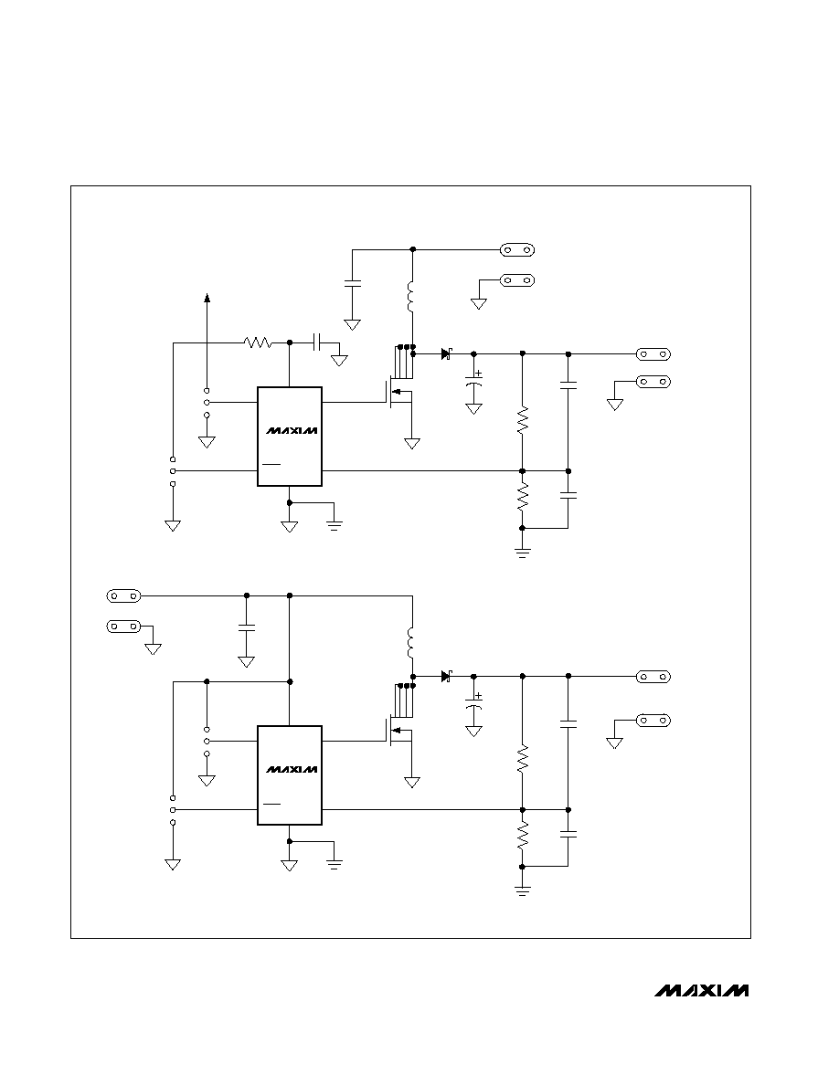
Figure 1. MAX1522 EV Kit Schematic
MAX1524
U1
MAX1522
U2
VOUT1
VIN2
GND2
1
2
3
JU2
1
2
3
JU1
3
4
5
2
R5
10
1
6
SET
EXT
SHDN
FB
V
CC
GND
C5
1
µF
C6
10
µF
L1
3.3
µH
3
5
6
2
1
D1
C9
33
µF
10V
VIN1
GND1
R1
301k
1%
R2
100k
1%
C1
100pF
C2
100pF
VOUT1 (+5V)
GND1
N1
R3
866k
1%
R4
100k
1%
C3
47pF
C4
330pF
VOUT2 (+12V)
GND2
C8
47
µF
20V
D2
L2
33
µH
3
5
6
2
1
N2
4
4
3
4
5
2
1
6
SET
EXT
SHDN
FB
V
CC
GND
C7
10
µF
1
2
3
JU4
1
2
3
JU3
GND2
Maxim cannot assume responsibility for use of any circuitry other than circuitry entirely embodied in a Maxim product. No circuit patent licenses are
implied. Maxim reserves the right to change the circuitry and specifications without notice at any time.
5 _____________________Maxim Integrated Products, 120 San Gabriel Drive, Sunnyvale, CA 94086 408-737-7600
© 2001 Maxim Integrated Products
Printed USA
is a registered trademark of Maxim Integrated Products.
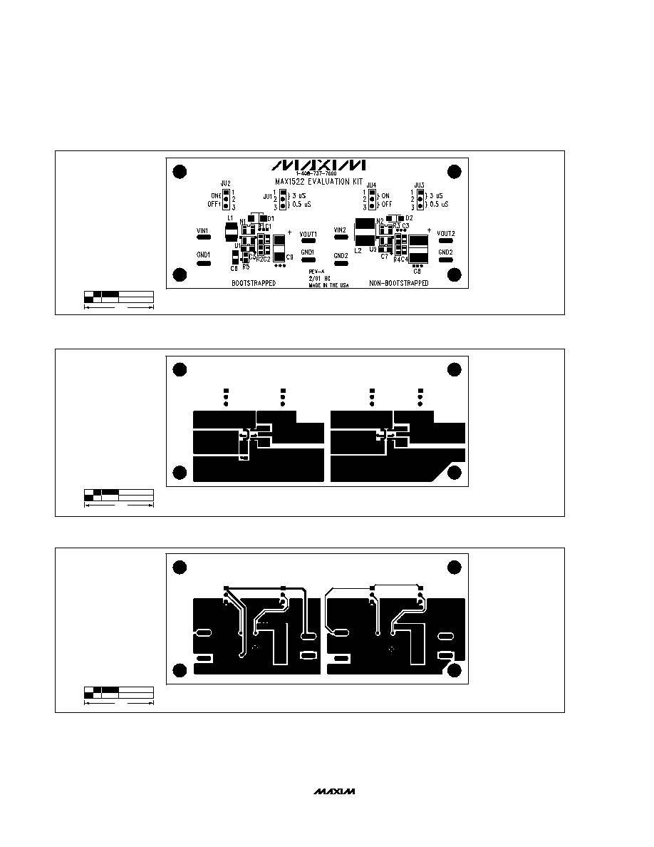
Figure 2. MAX1522 EV Kit Component Placement Guide--Component Side
1.0"
Figure 3. MAX1522 EV Kit PC Board Layout--Component Side
Figure 4. MAX1522 EV Kit PC Board Layout--Solder Side
MAX1522 Evaluation Kit
Evaluates: MAX1522/MAX1523/MAX1524
1.0"
1.0"