General Description
The MAX148/MAX149 10-bit data-acquisition systems
combine an 8-channel multiplexer, high-bandwidth
track/hold, and serial interface with high conversion
speed and low power consumption. They operate from a
single +2.7V to +5.25V supply, and sample to 133ksps.
Both devices' analog inputs are software configurable for
unipolar/bipolar and single-ended/differential operation.
The 4-wire serial interface connects directly to SPITM/
QSPITM and MICROWIRETM devices without external
logic. A serial-strobe output allows direct connection to
TMS320-family digital signal processors. The MAX148/
MAX149 use either the internal clock or an external serial-
interface clock to perform successive-approximation
analog-to-digital conversions.
The MAX149 has an internal 2.5V reference, while the
MAX148 requires an external reference. Both parts have
a reference-buffer amplifier with a ▒1.5% voltage-
adjustment range.
These devices provide a hard-wired SHDN pin and a
software-selectable power-down, and can be pro-
grammed to automatically shut down at the end of a con-
version. Accessing the serial interface automatically
powers up the MAX148/MAX149, and the quick turn-on
time allows them to be shut down between all conver-
sions. This technique can cut supply current to under
60ÁA at reduced sampling rates.
The MAX148/MAX149 are available in a 20-pin DIP and a
20-pin SSOP.
For 4-channel versions of these devices, see the
MAX1248/MAX1249 data sheet.
________________________Applications
Portable Data Logging
Data Acquisition
Medical Instruments
Battery-Powered Instruments
Pen Digitizers
Process Control
____________________________Features
o
8-Channel Single-Ended or 4-Channel
Differential Inputs
o
Single-Supply Operation: +2.7V to +5.25V
o
Internal 2.5V Reference (MAX149)
o
Low Power: 1.2mA (133ksps, 3V supply)
54ÁA (1ksps, 3V supply)
1ÁA (power-down mode)
o
SPI/QSPI/MICROWIRE/TMS320-Compatible
4-Wire Serial Interface
o
Software-Configurable Unipolar or Bipolar Inputs
o
20-Pin DIP/SSOP Packages
MAX148/MAX149
+2.7V to +5.25V, Low-Power, 8-Channel,
Serial 10-Bit ADCs
________________________________________________________________
Maxim Integrated Products
1
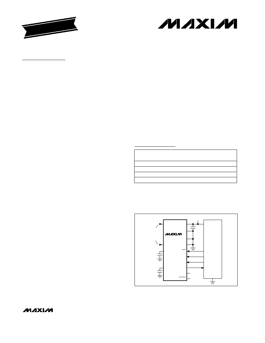
V
DD
I/O
SCK (SK)
MOSI (SO)
MISO (SI)
V
SS
SHDN
SSTRB
DOUT
DIN
SCLK
CS
COM
AGND
DGND
V
DD
CH7
4.7
Á
F
0.1
Á
F
CH0
0V TO
+2.5V
ANALOG
INPUTS
MAX149
CPU
+3V
VREF
0.01
Á
F
REFADJ
__________Typical Operating Circuit
19-0464; Rev 2; 5/98
PART
MAX148
ACPP
MAX148BCPP
MAX148ACAP
0░C to +70░C
0░C to +70░C
0░C to +70░C
TEMP. RANGE
PIN-PACKAGE
20 Plastic DIP
20 Plastic DIP
20 SSOP
EVALUATION KIT
AVAILABLE
Ordering Information
Ordering Information continued at end of data sheet.
Contact factory for availability of alternate surface-mount
packages.
MAX148BCAP
0░C to +70░C
20 SSOP
INL
(LSB)
▒1/2
▒1
▒1/2
▒1
SPI and QSPI are trademarks of Motorola, Inc. MICROWIRE is a trademark of National Semiconductor Corp.
Pin Configuration appears at end of data sheet.
For free samples & the latest literature: http://www.maxim-ic.com, or phone 1-800-998-8800.
For small orders, phone 408-737-7600 ext. 3468.
MAX148/MAX149
+2.7V to +5.25V, Low-Power, 8-Channel,
Serial 10-Bit ADCs
2
_______________________________________________________________________________________
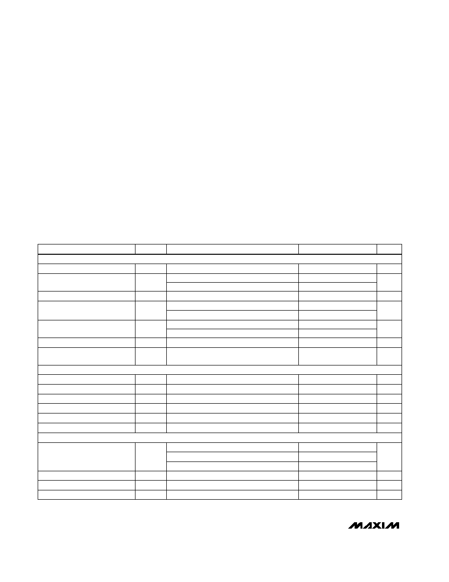
ABSOLUTE MAXIMUM RATINGS
ELECTRICAL CHARACTERISTICS
V
DD
= +2.7V to +5.25V; COM = 0V; f
SCLK
= 2.0MHz; external clock (50% duty cycle); 15 clocks/conversion cycle (133ksps);
MAX149--4.7ÁF capacitor at VREF pin; MAX148--external reference, VREF = 2.500 V applied to VREF pin; T
A
= T
MIN
to T
MAX
; unless
otherwise noted.)
Stresses beyond those listed under "Absolute Maximum Ratings" may cause permanent damage to the device. These are stress ratings only, and functional
operation of the device at these or any other conditions beyond those indicated in the operational sections of the specifications is not implied. Exposure to
absolute maximum rating conditions for extended periods may affect device reliability.
V
DD
to AGND, DGND................................................. -0.3V to 6V
AGND to DGND ...................................................... -0.3V to 0.3V
CH0¡CH7, COM to AGND, DGND ............ -0.3V to (V
DD
+ 0.3V)
VREF, REFADJ to AGND ........................... -0.3V to (V
DD
+ 0.3V)
Digital Inputs to DGND .............................................. -0.3V to 6V
Digital Outputs to DGND ........................... -0.3V to (V
DD
+ 0.3V)
Digital Output Sink Current .................................................25mA
Continuous Power Dissipation (T
A
= +70░C)
Plastic DIP (derate 11.11mW/░C above +70░C) ......... 889mW
SSOP (derate 8.00mW/░C above +70░C) ................... 640mW
CERDIP (derate 11.11mW/░C above +70░C) .............. 889mW
Operating Temperature Ranges
MAX148_C_P/MAX149_C_P .............................. 0░C to +70░C
MAX148_E_P/MAX149_E_P............................ -40░C to +85░C
MAX148_MJP/MAX149_MJP ........................ -55░C to +125░C
Storage Temperature Range ............................ -60░C to +150░C
Lead Temperature (soldering, 10sec) ............................ +300░C
Ás
1.5
t
ACQ
Differential Nonlinearity
Track/Hold Acquisition Time
ns
30
Aperture Delay
6
Ás
35
65
t
CONV
Conversion Time (Note 5)
5.5
7.5
ps
MHz
1.0
Full-Power Bandwidth
MHz
2.25
Small-Signal Bandwidth
dB
-75
Channel-to-Channel Crosstalk
dB
70
SFDR
Spurious-Free Dynamic Range
dB
-70
THD
Total Harmonic Distortion
dB
66
SINAD
Signal-to-Noise + Distortion Ratio
LSB
▒0.05
Channel-to-Channel Offset
Matching
ppm/░C
▒0.25
Gain Temperature Coefficient
▒0.5
<50
Bits
10
Resolution
Gain Error (Note 3)
▒1
Aperture Jitter
Offset Error
LSB
▒1.0
INL
Relative Accuracy (Note 2)
LSB
▒1
DNL
▒0.15
▒1
LSB
▒0.15
▒2
UNITS
MIN
TYP
MAX
SYMBOL
PARAMETER
External clock = 2MHz, 12 clocks/conversion
Internal clock, SHDN = V
DD
Internal clock, SHDN = FLOAT
MAX14_A
-3dB rolloff
65kHz, 2.500V
p-p
(Note 4)
Up to the 5th harmonic
MAX14_A
MAX14_B
No missing codes over temperature
MAX14_A
MAX14_B
CONDITIONS
LSB
▒2
MAX14_B
DC ACCURACY
(Note 1)
DYNAMIC SPECIFICATIONS
(10kHz sine-wave input, 0V to 2.500Vp-p, 133ksps, 2.0MHz external clock, bipolar input mode)
CONVERSION RATE
MAX148/MAX149
+2.7V to +5.25V, Low-Power, 8-Channel,
Serial 10-Bit ADCs
_______________________________________________________________________________________
3
Multiplexer Leakage Current
ÁA
0.01
10
Shutdown VREF Input Current
k
18
25
VREF Input Resistance
ÁA
100
150
VREF Input Current
V
1.0
V
DD
+
50mV
VREF Input Voltage Range
(Note 9)
pF
16
Input Capacitance
1.8
MHz
0.225
Internal Clock Frequency
ÁA
▒0.01
▒1
UNITS
MIN
TYP
MAX
SYMBOL
PARAMETER
SHDN = FLOAT
VREF = 2.500V
SHDN = V
DD
On/off leakage current, V
CH_
= 0V or V
DD
CONDITIONS
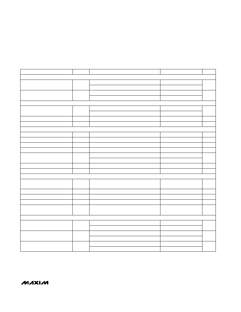
ELECTRICAL CHARACTERISTICS (continued)
V
DD
= +2.7V to +5.25V; COM = 0V; f
SCLK
= 2.0MHz; external clock (50% duty cycle); 15 clocks/conversion cycle (133ksps);
MAX149--4.7ÁF capacitor at VREF pin; MAX148--external reference, VREF = 2.500 V applied to VREF pin; T
A
= T
MIN
to T
MAX
; unless
otherwise noted.)
V
2.470
2.500
2.530
VREF Output Voltage
T
A
= +25░C (Note 7)
mA
30
VREF Short-Circuit Current
▒30
MAX149
mV
0.35
Load Regulation (Note 8)
0mA to 0.2mA output load
0
Internal compensation mode
ÁF
4.7
Capacitive Bypass at VREF
External compensation mode
ÁF
0.01
Capacitive Bypass at REFADJ
%
▒1.5
REFADJ Adjustment Range
V
V
DD
-
0.5
REFADJ Buffer-Disable Threshold
ÁF
0
Capacitive Bypass at VREF
Internal compensation mode
2.00
V/V
2.06
Reference Buffer Gain
4.7
MAX148
MAX149
External compensation mode
▒10
ÁA
▒50
REFADJ Input Current
MAX148
MAX149
ppm/░C
VREF Temperature Coefficient
0 to VREF
V
▒VREF / 2
Input Voltage Range, Single-
Ended and Differential (Note 6)
Unipolar, COM = 0V
Bipolar, COM = VREF / 2
0.1
2.0
MHz
0
2.0
External Clock Frequency
Data transfer only
CONVERSION RATE (continued)
ANALOG/COM INPUTS
INTERNAL REFERENCE
(MAX149 only, reference buffer enabled)
EXTERNAL REFERENCE AT VREF
(Buffer disabled)
EXTERNAL REFERENCE AT REFADJ
I
DD
MAX148/MAX149
+2.7V to +5.25V, Low-Power, 8-Channel,
Serial 10-Bit ADCs
4
_______________________________________________________________________________________
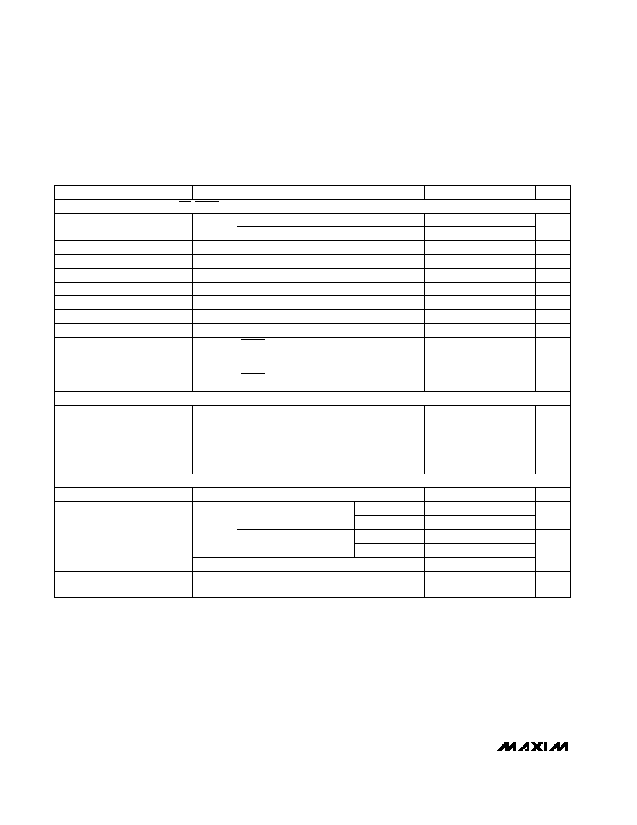
ELECTRICAL CHARACTERISTICS (continued)
V
DD
= +2.7V to +5.25V; COM = 0V; f
SCLK
= 2.0MHz; external clock (50% duty cycle); 15 clocks/conversion cycle (133ksps);
MAX149--4.7ÁF capacitor at VREF pin; MAX148--external reference, VREF = 2.500 V applied to VREF pin; T
A
= T
MIN
to T
MAX
; unless
otherwise noted.)
V
3.0
V
IH
DIN, SCLK, CS Input High Voltage
V
DD
> 3.6V
mV
▒0.3
PSR
Supply Rejection (Note 12)
Full-scale input, external reference = 2.500V,
V
DD
= 2.7V to 5.25V
pF
15
C
IN
DIN, SCLK, CS Input Capacitance
ÁA
▒0.01
▒1
I
IN
DIN, SCLK, CS Input Leakage
V
0.2
V
HYST
DIN, SCLK, CS Input Hysteresis
V
0.8
V
IL
DIN, SCLK, CS Input Low Voltage
2.0
ÁA
▒4.0
I
S
SHDN Input Current
V
0.4
V
SL
SHDN Input Low Voltage
V
V
DD
- 0.4
V
SH
SHDN Input High Voltage
SHDN = 0V or V
DD
nA
▒100
SHDN Maximum Allowed
Leakage, Mid Input
V
V
DD
/ 2
V
FLT
SHDN Voltage, Floating
SHDN = FLOAT
SHDN = FLOAT
UNITS
MIN
TYP
MAX
SYMBOL
PARAMETER
(Note 10)
V
IN
= 0V or V
DD
V
DD
3.6V
CONDITIONS
ÁA
▒0.01
▒10
I
L
Three-State Leakage Current
V
V
DD
- 0.5
V
OH
Output Voltage High
V
0.8
V
OL
Output Voltage Low
0.4
pF
15
C
OUT
Three-State Output Capacitance
CS = V
DD
(Note 10)
CS = V
DD
I
SOURCE
= 0.5mA
I
SINK
= 16mA
I
SINK
= 5mA
2.70
5.25
1.2
2.0
Operating mode,
full-scale input (Note 11)
3.5
15
Full power-down
1.2
10
mA
1.6
3.0
V
1.1
V
DD
- 1.1
V
SM
SHDN Input Mid Voltage
Positive Supply Current
V
DD
Positive Supply Voltage
V
I
DD
ÁA
30
70
DIGITAL INPUTS
(DIN, SCLK, CS, SHDN)
DIGITAL OUTPUTS
(DOUT, SSTRB)
POWER REQUIREMENTS
Fast power-down (MAX149)
I
DD
V
DD
= 5.25V
V
DD
= 3.6V
V
DD
= 5.25V
V
DD
= 3.6V
MAX148/MAX149
+2.7V to +5.25V, Low-Power, 8-Channel,
Serial 10-Bit ADCs
_______________________________________________________________________________________
5
Figure 1
__________________________________________Typical Operating Characteristics
(V
DD
= 3.0V, VREF = 2.500V, f
SCLK
= 2.0MHz, C
LOAD
= 20pF, T
A
= +25░C, unless otherwise noted.)
0
256
512
768
1024
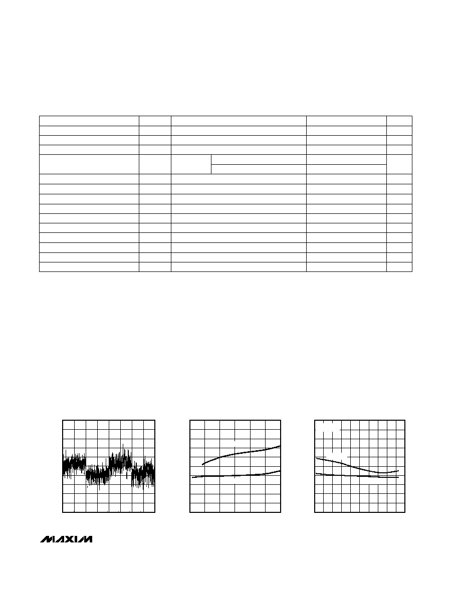
INTEGRAL NONLINEARITY
vs. CODE
0.10
0.05
-0.10
-0.05
0
MAX148/9-01
CODE
INL (LSB)
0.125
0
2.25
2.75
4.25
INTEGRAL NONLINEARITY
vs. SUPPLY VOLTAGE
0.100
0.075
0.050
0.025
SUPPLY VOLTAGE (V)
INL (LSB)
3.75
5.25
3.25
4.75
MAX148/9-02
MAX149
MAX148
0
0.025
0.050
0.075
0.100
0.125
-60
-20
20
60
100
140
INTEGRAL NONLINEARITY
vs. TEMPERATURE
TEMPERATURE
(░C)
INL (LSB)
MAX148/9-03
MAX148
MAX149
V
DD
= 2.7V
TIMING CHARACTERISTICS
(V
DD
= +2.7V to +5.25V, T
A
= T
MIN
to T
MAX
, unless otherwise noted.)
Note 1:
Tested at V
DD
= 2.7V; COM = 0V; unipolar single-ended input mode.
Note 2:
Relative accuracy is the deviation of the analog value at any code from its theoretical value after the full-scale range has
been calibrated.
Note 3:
MAX149--internal reference, offset nulled; MAX148--external reference (VREF = +2.500V), offset nulled.
Note 4:
Ground "on" channel; sine wave applied to all "off" channels.
Note 5:
Conversion time defined as the number of clock cycles multiplied by the clock period; clock has 50% duty cycle.
Note 6:
The common-mode range for the analog inputs is from AGND to V
DD
.
Note 7:
Sample tested to 0.1% AQL.
Note 8:
External load should not change during conversion for specified accuracy.
Note 9:
ADC performance is limited by the converter's noise floor, typically 300ÁVp-p.
Note 10:
Guaranteed by design. Not subject to production testing.
Note 11:
The MAX148 typically draws 400ÁA less than the values shown.
Note 12:
Measured as
|
V
FS
(2.7V) - V
FS
(5.25V)
|
.
Internal clock mode only (Note 7)
External clock mode only, Figure 2
External clock mode only, Figure 1
DIN to SCLK Setup
Figure 1
Figure 2
Figure 1
MAX14_ _C/E
CONDITIONS
MAX14_ _M
ns
20
240
Figure 1
ns
t
CSH
ns
240
t
STR
CS Rise to SSTRB Output Disable
ns
240
t
SDV
CS Fall to SSTRB Output Enable
240
t
SSTRB
SCLK Fall to SSTRB
ns
200
t
CL
SCLK Pulse Width Low
ns
200
SCLK Pulse Width High
ns
0
CS to SCLK Rise Hold
ns
100
t
CSS
CS to SCLK Rise Setup
ns
240
t
TR
CS Rise to Output Disable
ns
240
t
DV
CS Fall to Output Enable
t
CH
20
200
t
DO
SCLK Fall to Output Data Valid
ns
0
t
DH
DIN to SCLK Hold
ns
Ás
1.5
t
ACQ
Acquisition Time
0
t
SCK
SSTRB Rise to SCLK Rise
ns
100
t
DS
UNITS
MIN
TYP
MAX
SYMBOL
PARAMETER