
_______________General Description
The MAX1488E quad, low-power line driver is designed
for EIA/TIA-232, EIA/TIA-562, and CCITT V.28 commu-
nications in harsh environments. Each transmitter out-
put is protected against ±15kV electrostatic discharge
(ESD) shocks. The inputs are TTL and CMOS compati-
ble with minimal loading. The outputs feature internally
controlled slew-rate limiting and current limiting. This
device has a guaranteed 120kbps data rate. Power-
supply current is less than 180µA over a ±4.5V to
±13.2V supply voltage range.
The MAX1488E is pin compatible with the MC1488,
MC14C88, SN75188, SN75C188, DS1488, and
DS14C88. It is available in 14-pin plastic DIP and SO
packages.
________________________Applications
PC Motherboards
Modems
Interface Data Terminal Equipment (DTE) with
Data Circuit-Terminating Equipment (DCE)
Equipment Meeting IEC1000-4-2
(formerly IEC801-2) or ±15kV ESD Protection
____________________________Features
o
ESD Protection:
±15kV--Human Body Model
±6kV--IEC801-2, Contact Discharge
±15kV--IEC801-2, Air-Gap Discharge
o
Latchup Free, Even During an ESD Event
o
Low 85µA Supply Current from I
EE
or I
CC
o
Guaranteed 120kbps Data Rate
o
No External Capacitors Required for Slew-Rate
Limiting
o
Pin Compatible with MC1488, MC14C88, SN75188,
SN75C188, DS1488, and DS14C88
MAX1488E
±15kV ESD-Protected, Quad, Low-Power
RS-232 Line Driver
________________________________________________________________
Maxim Integrated Products
1
14
13
12
11
10
9
8
1
2
3
4
5
6
7
V
CC
INPUT D1
INPUT D2
OUTPUT D
INPUT C1
INPUT C2
OUTPUT C
V
EE
INPUT A
OUTPUT A
INPUT B1
INPUT B2
OUTPUT B
GND
TOP VIEW
MAX1488E
DIP/SO
__________________Pin Configuration
INTERCONNECTING
CABLE
SIGNAL GROUND
TTL/CMOS
LOGIC
PC
MOTHERBOARD
(DTE)
MODEM
(DCE)
TTL/CMOS
LOGIC
1
/
4
MAX1488E
1
/
4
MAX1489E
1
/
4
MAX1489E
1
/
4
MAX1488E
__________Typical Operating Circuit
Call toll free 1-800-998-8800 for free samples or literature.
19-2403; Rev 0; 8/95
PART
MAX1488ECPD
MAX1488ECSD
MAX1488EC/D
0°C to +70°C
0°C to +70°C
0°C to +70°C
TEMP. RANGE
PIN-PACKAGE
14 Plastic DIP
14 SO
Dice*
______________Ordering Information
* Dice are specified at T
A
= +25°C.
MAX1488EEPD
MAX1488EESD
-40°C to +85°C
-40°C to +85°C
14 Plastic DIP
14 SO
MAX1488E
±15kV ESD-Protected, Quad, Low-Power
RS-232 Line Driver
2
_______________________________________________________________________________________
ABSOLUTE MAXIMUM RATINGS
ELECTRICAL CHARACTERISTICS
(V
CC
= 4.5V to 13.2V, V
EE
= -4.5V to -13.2V, T
A
= T
MIN
to T
MAX
, unless otherwise noted. Typical values are at T
A
= +25°C.)
Stresses beyond those listed under "Absolute Maximum Ratings" may cause permanent damage to the device. These are stress ratings only, and functional
operation of the device at these or any other conditions beyond those indicated in the operational sections of the specifications is not implied. Exposure to
absolute maximum rating conditions for extended periods may affect device reliability.
Positive Supply Voltage (V
CC
) .............................................+14V
Negative Supply Voltage (V
EE
) .............................................-14V
Input Voltage (V
IN
) .................................................-0.3V to +15V
Driver Output Voltage ..........................................................±15V
Continuous Power Dissipation (T
A
= +70°C)
Plastic DIP (derate 10.00mW/°C above +70°C) ..........800mW
SO (derate 8.7mW/°C above +70°C) ...........................695mW
Operating Temperature Ranges
MAX1488EC_D ...................................................0°C to +70°C
MAX1488EE_D ................................................-40°C to +85°C
Storage Temperature Range .............................-65°C to +160°C
Lead Temperature (soldering, 10sec) .............................+300°C
Output shorted to ground (Note 1)
No load
V
CC
= V
EE
= 0V
I
V
O
I
2.0V
No load
CONDITIONS
300
R
O
Output Resistance
µA
0
±2
I
IN1
Input Current
V
0.8
V
IL
Input Low Voltage
V
2.0
V
IH
Input High Voltage
mA
±4
±20
±45
I
OS
Output Short-Circuit Current
µA
-180
-85
I
EE
Negative Supply Current
4.5
13.2
V
CC
V
-13.2
-4.5
V
EE
Operating Voltage Range
µA
85
180
I
CC
Positive Supply Current
UNITS
MIN
TYP
MAX
SYMBOL
PARAMETER
V
CC
= -V
EE
= 5.0V, R
L
= 3k
V
3.7
4.0
V
OH
Output Voltage High
V
CC
= 12.0V, V
EE
= -12.0V, C
L
= 50pF
V
CC
= 9.0V, V
EE
= -9.0V, C
L
= 50pF
V
CC
= 4.5V, V
EE
= -4.5V, C
L
= 50pF
µs
3.1
4.2
t
PLH
2.8
3.9
2.4
3.5
V
CC
= 12.0V, V
EE
= -12.0V, C
L
= 50pF
V
CC
= 9.0V, V
EE
= -9.0V, C
L
= 50pF
V
CC
= 4.5V, V
EE
= -4.5V, C
L
= 50pF
µs
2.6
5.4
t
PHL
2.4
5.1
2.1
4.5
Output Propagation Delay,
Low to High
Output Propagation Delay,
High to Low
V
CC
= 12.0V, V
EE
= -12.0V, C
L
= 50pF
V
CC
= 9.0V, V
EE
= -9.0V, C
L
= 50pF
V
CC
= 4.5V, V
EE
= -4.5V, C
L
= 50pF
µs
0.42
t
SK
0.42
0.25
Propagation Delay Skew,
I
t
PLH
- t
PHL
I
ESD CHARACTERISTICS
±15
Human Body Model
IEC-1000-4-2 (Contact Discharge)
±6
IEC-1000-4-2 (Air-Gap Discharge)
kV
±15
ESD Protection
DC CHARACTERISTICS
TIMING CHARACTERISTICS (see Figure 1)
Output Voltage Low
V
OL
V
-4.5
-3.7
10
10.5
5
5.4
13.2
-10.8
-10
-5.8
-5
-13.2
V
CC
= -V
EE
= 5.0V, R
L
= 3k
V
CC
= -V
EE
= 13.2V, R
L
= open
V
CC
= -V
EE
= 13.2V, R
L
= open
V
CC
= -V
EE
= 12.0V, R
L
= 3k
V
CC
= -V
EE
= 6.5V, R
L
= 3k
V
CC
= -V
EE
= 12.0V, R
L
= 3k
V
CC
= -V
EE
= 6.5V, R
L
= 3k
MAX1488E
±15kV ESD-Protected, Quad, Low-Power
RS-232 Line Driver
_______________________________________________________________________________________
3
Note 1:
The I
OS
value is for one output at a time. If more than one output is shorted simultaneously, damage may occur.
ELECTRICAL CHARACTERISTICS (continued)
(V
CC
= 4.5V to 13.2V, V
EE
= -4.5V to -13.2V, T
A
= T
MIN
to T
MAX
, unless otherwise noted. Typical values are at T
A
= +25°C.)
C
L
= 1500pF, R
L
= 5k
,
V
OUTPUT_
from -3.3V to 3.3V
850
t
R1
C
L
= 15pF to 2500pF, R
L
= 3k
to 7k
,
V
CC
= 12V, V
EE
= -12V, T
A
= +25°C
C
L
= 15pF to 2500pF, R
L
= 3k
to 7k
,
V
CC
= 12V, V
EE
= -12V, T
A
= +25°C,
V
OUTPUT_
from -3.0V to 3.0V
C
L
= 1500pF, R
L
= 5k
,
V
OUTPUT_
from -3.0V to 3.0V
C
L
= 1500pF, R
L
= 5k
,
V
OUTPUT_
from -3.3V to 3.3V
C
L
= 1500pF, R
L
= 5k
,
V
OUTPUT_
from -3.0V to 3.0V
CONDITIONS
kbps
120
Guaranteed Data Rate
V/µs
4
30
SR
Output Slew Rate
ns
765
t
F2
Output Fall Time
860
t
F1
ns
740
t
R2
Output Rise Time
UNITS
MIN
TYP
MAX
SYMBOL
PARAMETER
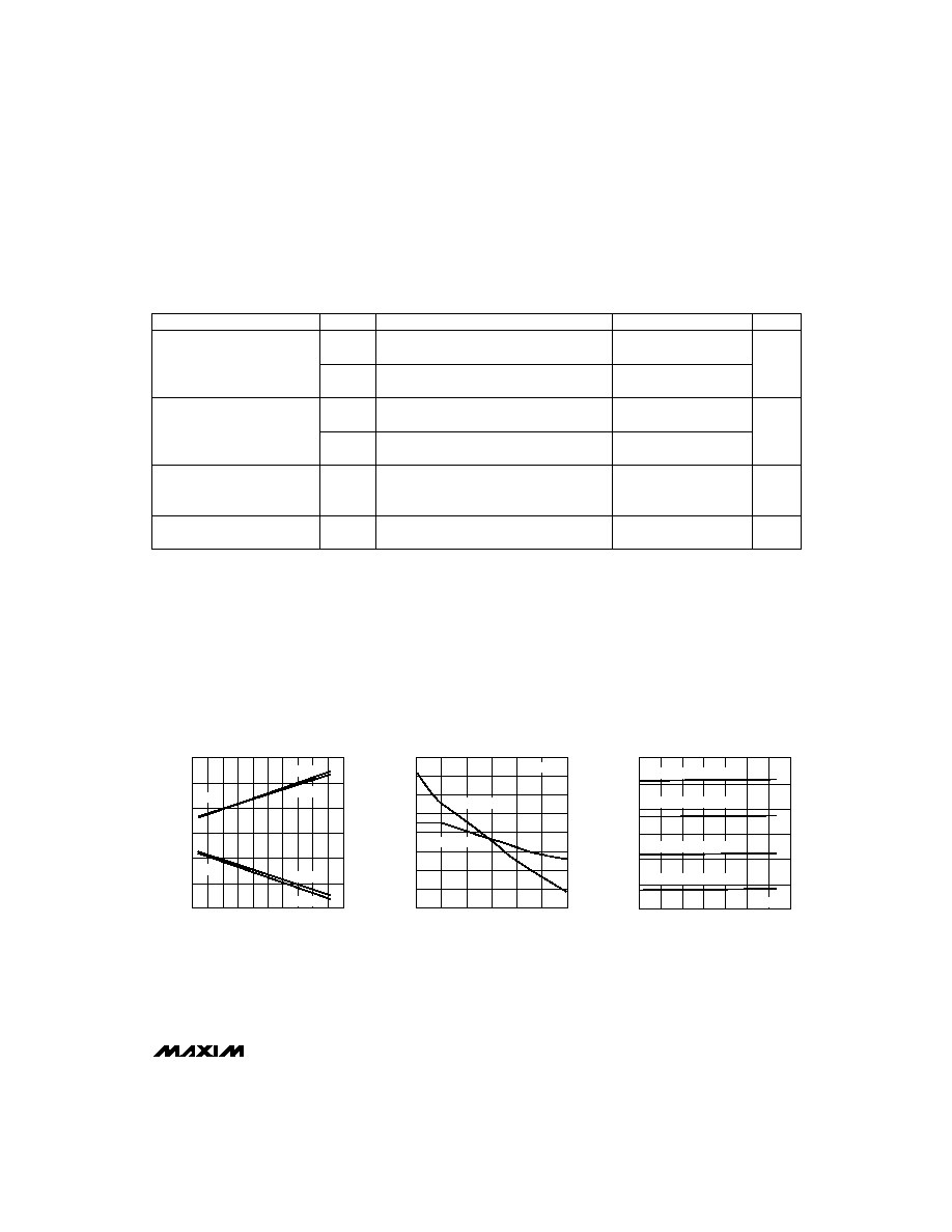
__________________________________________Typical Operating Characteristics
(V
CC
= 12V, V
EE
= -12V, T
A
= +25°C, unless otherwise noted.)
15
10
-15
4
OUTPUT VOLTAGE
vs. SUPPLY VOLTAGE
5
MAX1488E TOC-1
V
CC
AND -V
EE
SUPPLIES (V)
OUTPUT VOLTAGE (V)
10
-5
-10
6
8
14
0
12
5
11
7
9
13
V
OH
R
L
= 3k
R
L
= 3k
R
L
= 5k
R
L
= 5k
V
OL
9
8
11
10
3
0
SLEW RATE vs.
LOAD CAPACITANCE
7
MAX1488E TOC-2
LOAD CAPACITANCE (pF)
SLEW RATE (V/
µ
s)
1500
5
4
500
1000
6
2500
2000
3000
RISING EDGE
FALLING EDGE
R
L
= 3k
15
10
-15
-40
OUTPUT VOLTAGE
vs. TEMPERATURE
5
MAX1488E TOC-3
TEMPERATURE (°C)
OUTPUT VOLTAGE (V)
20
-5
-10
-20
0
100
0
60
40
80
V
OH
@ V
CC
= -V
EE
= 12V
V
OH
@ V
CC
= -V
EE
= 4.5V
V
OL
@ V
CC
= -V
EE
= 4.5V
V
OL
@ V
CC
= -V
EE
= 12V
R
L
= 3k

MAX1488E
_______________Detailed Description
The MAX1488E provides ±15kV of ESD protection when
operating or when powered down. After an ESD event,
the MAX1488E will not latch up. Internal slew-rate-limit-
ing circuitry eliminates the need for external capacitors.
The MAX1488E has a guaranteed 120kbps data rate.
Outputs
Tables 1 and 2 describe the output states. The output
voltage level is affected by both the load current and
supply voltage, and is stable over temperature. Refer to
the
Typical Operating Characteristics to see how the
output voltage varies with supply voltage, load capaci-
tance, and temperature.
Table 1. Driver A Functions
Table 2. Driver BD Functions
Inputs
The driver inputs determine the driver output states
(Tables 1 and 2). Driver inputs B, C, and D have two
inputs.
Connect unused inputs to ground or V
CC
.
±15kV ESD Protection
As with all Maxim devices, ESD-protection structures
are incorporated on all pins to protect against electro-
static discharges encountered during handling and
assembly. The MAX1488E driver outputs have extra
protection against static electricity found in normal
operation. Maxim's engineers developed state-of-the-
art structures to protect these pins against ESD of
±15kV, without damage. After an ESD event, the
MAX1488E keeps working without latchup.
ESD protection can be tested in various ways; the
transmitter outputs are characterized for protection to
the following:
1) ±15kV using the Human Body Model
2) ±6kV using the Contact-Discharge Method specified
in IEC1000-4-2 (formerly IEC801-2)
3) ±15kV using the Air-Gap Method specified in
IEC1000-4-2 (formerly IEC801-2).
ESD Test Conditions
ESD performance depends on a number of conditions.
Contact Maxim for a reliability report that documents
test setup, methodology, and results.
Human Body Model
Figure 2a shows the Human Body Model, and Figure
2b shows the current waveform it generates when dis-
charged into a low impedance. This model consists of
a 100pF capacitor charged to the ESD voltage of inter-
est, which is then discharged into the test device
through a 1.5k
resistor.
±15kV ESD-Protected, Quad, Low-Power
RS-232 Line Driver
4
_______________________________________________________________________________________
_____________________Pin Description
NAME
FUNCTION
1
V
EE
-4.5V to -13.2V Supply Voltage Input
2, 4, 5, 9,
10, 12, 13
INPUT_
Driver Inputs
PIN
3, 6, 8, 11
OUTPUT_
Driver Outputs
7
GND
Ground
14
V
CC
+4.5V to +13.2V Supply Voltage Input
t
F2
t
F1
T
PHL
T
PLH
t
R1
t
R2
1.5V
3.0V
0V
0V
DRIVER
INPUT
V
OUT
V
OH
V
OL
3.3V
3.0V
-3.0V
-3.3V
R
L
C
L
SIGNAL
GENERATOR
Figure 1. Slew-Rate Test Circuit and Timing Diagram
INPUT A
OUTPUTA
H
L
L
H
INPUT_1
INPUT_2
OUTPUT_
H
H
L
L
X
H
X
L
H

IEC1000-4-2
The IEC1000-4-2 standard covers ESD testing and per-
formance of finished equipment; it does not specifically
refer to integrated circuits. The MAX1488E helps you
design equipment that meets Level 4 (the highest level)
of IEC1000-4-2, without additional ESD-protection com-
ponents.
The major difference between tests done using the
Human Body Model and IEC1000-4-2 is higher peak
current in IEC1000-4-2. Because series resistance is
lower in the IEC1000-4-2 ESD test model (Figure 3a),
the ESD withstand voltage measured to this standard is
generally lower than that measured using the Human
Body Model. Figure 3b shows the current waveform for
the ±6kV IEC1000-4-2 Level 4 ESD Contact-Discharge
test.
The Air-Gap test involves approaching the device with
a charged probe. The Contact-Discharge method con-
nects the probe to the device before the probe is ener-
gized.
Machine Model
The Machine Model for ESD testing uses a 200pF stor-
age capacitor and zero-discharge resistance. Its objec-
tive is to mimic the stress caused by contact that
occurs with handling and assembly during manufactur-
ing. Of course, all pins (not just RS-232 inputs and out-
puts) require this protection during manufacturing.
Therefore, the Machine Model is less relevant to the I/O
ports than the Human Body Model and IEC1000-4-2.
__________Applications Information
Use proper layout to ensure other devices on your
board are not damaged in an ESD strike. Currents as
high as 60A can instantaneously pass into the ground,
so it is important to minimize the ground-lead return
path to the power supply. A separate return path to the
power supply is recommended. Trace widths should be
greater than 40 mils. V
CC
and V
EE
must be bypassed
with 0.1µF capacitors as close to the part as possible to
ensure maximum ESD protection.
MAX1488E
±15kV ESD-Protected, Quad, Low-Power
RS-232 Line Driver
_______________________________________________________________________________________
5
CHARGE-CURRENT
LIMIT RESISTOR
DISCHARGE
RESISTANCE
STORAGE
CAPACITOR
Cs
100pF
R
C
1M
R
D
1500
HIGH-
VOLTAGE
DC
SOURCE
DEVICE
UNDER
TEST
Figure 2a. Human Body ESD Test Model
I
P
100%
90%
36.8%
t
RL
TIME
t
DL
CURRENT WAVEFORM
PEAK-TO-PEAK RINGING
(NOT DRAWN TO SCALE)
Ir
10%
0
0
AMPERES
Figure 2b. Human Body Model Current Waveform
CHARGE-CURRENT
LIMIT RESISTOR
DISCHARGE
RESISTANCE
STORAGE
CAPACITOR
Cs
150pF
R
C
50M to 100M
R
D
330
HIGH-
VOLTAGE
DC
SOURCE
DEVICE
UNDER
TEST
Figure 3a. IEC1000-4-2 ESD Test Model
t
r
= 0.7ns to 1ns
30ns
60ns
t
100%
90%
10%
I
PEAK
I
Figure 3b. IEC1000-4-2 ESD Generator Current Waveform