Äîêóìåíòàöèÿ è îïèñàíèÿ www.docs.chipfind.ru
General Description
The MAX1421 is a +3.3V, 12-bit analog-to-digital con-
verter (ADC), featuring a fully-differential input,
pipelined, 12-stage ADC architecture with wideband
track-and-hold (T/H) and digital error correction incor-
porating a fully-differential signal path. The MAX1421 is
optimized for low-power, high-dynamic performance
applications in imaging and digital communications.
The converter operates from a single +3.3V supply,
consuming only 188mW while delivering a typical sig-
nal-to-noise ratio (SNR) of 66dB at an input frequency
of 15MHz and a sampling frequency of 40Msps. The
fully-differential input stage has a small signal -3dB
bandwidth of 400MHz and may be operated with sin-
gle-ended inputs.
An internal +2.048V precision bandgap reference sets
the full-scale range of the ADC. A flexible reference
structure accommodates an internal or externally
applied buffered or unbuffered reference for applica-
tions requiring increased accuracy or a different input
voltage range.
In addition to low operating power, the MAX1421 fea-
tures two power-down modes, a reference power-down
and a shutdown mode. In reference power-down, the
internal bandgap reference is deactivated, resulting in
a typical 2mA supply current reduction. For idle peri-
ods, a full shutdown mode is available to maximize
power savings.
The MAX1421 provides parallel, offset binary, CMOS-
compatible three-state outputs.
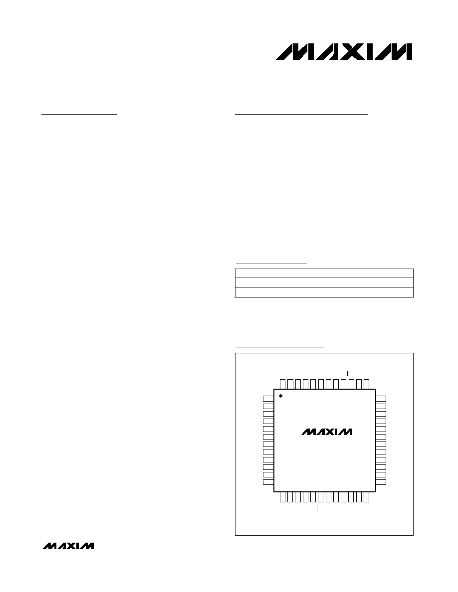
The MAX1421 is available in a 7mm x 7mm, 48-pin
TQFP package, and is specified over the commercial
(0°C to +70°C) and the extended industrial (-40°C to
+85°C) temperature ranges.
Pin-compatible higher- and lower-speed versions of the
MAX1421 are also available. Please refer to the
MAX1420 data sheet for a frequency of 60Msps and
the MAX1422 data sheet for a frequency of 20Msps.
________________________Applications
Medical Ultrasound Imaging
CCD Pixel Processing
Data Acquisition
Radar
IF and Baseband Digitization
Features
o Single +3.3V Power Supply
o 67dB SNR at f
IN
= 5MHz
o 66dB SNR at f
IN
= 15MHz
o Internal, +2.048V Precision Bandgap Reference
o Differential, Wideband Input T/H Amplifier
o Power-Down Modes
180mW (Reference Shutdown Mode)
10µW (Shutdown Mode)
o Space-Saving 48-Pin TQFP Package
MAX1421
12-Bit, 40Msps, +3.3V, Low-Power ADC
with Internal Reference
________________________________________________________________ Maxim Integrated Products
1
D9
D8
D7
D6
DV
DD
DV
DD
DGND
DGND
D5
D4
D3
D2
AGND
AV
DD
AV
DD
AGND
AGND
INP
INN
AGND
AGND
AV
DD
AV
DD
AGND
1
2
3
4
5
6
7
8
9
10
11
12
36
35
34
33
32
31
30
29
28
27
26
25
48-TQFP
MAX1421
AGND
AV
DD
AV
DD
AGND
CLK
CLK
AGND
AV
DD
DV
DD
DGND
D0
D1
13
14
15
16
17
18
19
20
21
22
23
24
48
47
46
45
44
43
42
41
40
39
38
37
AGND
AV
DD
CML
REFN
REFP
REFIN
AV
DD
AGND
PD
OE
D11
D10
Pin Configuration
19-1900; Rev 0; 5/01
Ordering Information
48 TQFP
PIN-PACKAGE
TEMP. RANGE
0°C to +70°C
MAX1421CCM
PART
Functional Diagram appears at end of data sheet.
48 TQFP
-40°C to +85°C
MAX1421ECM
For pricing, delivery, and ordering information, please contact Maxim/Dallas Direct! at
1-888-629-4642, or visit Maxim's website at www.maxim-ic.com.
MAX1421
12-Bit, 40Msps, +3.3V, Low-Power ADC
with Internal Reference
2
_______________________________________________________________________________________
ABSOLUTE MAXIMUM RATINGS
ELECTRICAL CHARACTERISTICS
(V
AVDD
= V
DVDD
= +3.3V, AGND = DGND = 0, V
IN
= ±1.024V, differential input voltage at -0.5dB FS, internal reference,
f
CLK
= 40MHz (50% duty cycle), digital output load C
L
10pF, T
A
= T
MIN
to T
MAX
, unless otherwise noted. Typical values are at
T
A
= +25°C.)
Stresses beyond those listed under "Absolute Maximum Ratings" may cause permanent damage to the device. These are stress ratings only, and functional
operation of the device at these or any other conditions beyond those indicated in the operational sections of the specifications is not implied. Exposure to
absolute maximum rating conditions for extended periods may affect device reliability.
AV
DD
, DV
DD
to AGND ..............................................-0.3V to +4V
DV
DD
, AV
DD
to DGND..............................................-0.3V to +4V
DGND to AGND.....................................................-0.3V to +0.3V
INP, INN, REFP, REFN, REFIN,
CML, CLK, CLK,....................(AGND - 0.3V) to (AV
DD
+ 0.3V)
D0D11, OE, PD .......................(DGND - 0.3V) to (DV
DD
+ 0.3V)
Continuous Power Dissipation (T
A
= +70°C)
48-Pin TQFP (derate 12.5mW/°C above +70°C)........1000mW
Maximum Junction Temperature .....................................+150°C
Operating Temperature Ranges
MAX1421CCM ...................................................0°C to +70°C
MAX1421ECM ................................................-40°C to +85°C
Storage Temperature Range .............................-65°C to +150°C
Lead Temperature (soldering, 10s) .................................+300°C
PARAMETER
SYMBOL
CONDITIONS
MIN
TYP
MAX
UNITS
DC ACCURACY
Resolution
RES
12
Bits
T
A
= +25
°C, no missing codes
-1
1
Differential Nonlinearity
DNL
T
A
= T
MIN
to T
MAX
±0.5
LSB
Integral Nonlinearity
INL
T
A
= T
MIN
to T
MAX
±2
LSB
Mid-scale Offset
MSO
-3
±.75
3
%FSR
Mid-scale Offset Temperature
Coefficient
MSOTC
3
10
-4
%/
°C
Internal reference (Note 1)
-5
0.1
5
External reference applied to REFIN (Note 2)
-5
±3
5
Gain Error
GE
External reference applied to REFP, CML,
and REFN (Note 3)
-1.5
±0.5
1.5
%FSR
Gain Error Temperature
Coefficient
GETC
External reference applied to REFP, CML,
and REFN, (Note 3)
15
10
-6
%/
°C
DYNAMIC PERFORMANCE (f
CLK
= 40MHz, 4096-point FFT)
f
IN
= 5MHz
67
Signal-to-Noise Ratio
SNR
f
IN
= 15MHz, T
A
= +25
°C
62
66
dB
f
IN
= 5MHz
73
Spurious-Free Dynamic Range
SFDR
f
IN
= 15MHz, T
A
= +25
°C
64
70
dBc
f
IN
= 5MHz
-74
Total Harmonic Distortion
THD
f
IN
= 15MHz, T
A
= +25
°C
-69
-62
dBc
f
IN
= 5MHz
66
Signal-To-Noise Plus Distortion
SINAD
f
IN
= 15MHz, T
A
= +25
°C
60
63.5
dB
f
IN
= 5MHz
10.7
Effective Number of Bits
ENOB
f
IN
= 15MHz, T
A
= +25
°C
60
10.3
Bits
Two-Tone Intermodulation
Distortion
IMD
TT
f
IN1
= 11.569MHz, f
IN2
= 13.445MHz
(Note 4)
-80
dBc
MAX1421
12-Bit, 40Msps, +3.3V, Low-Power ADC
with Internal Reference
_______________________________________________________________________________________
3
ELECTRICAL CHARACTERISTICS (continued)
(V
AVDD
= V
DVDD
= +3.3V, AGND = DGND = 0, V
IN
= ±1.024V, differential input voltage at -0.5dB FS, internal reference,
f
CLK
= 40MHz (50% duty cycle), digital output load C
L
10pF, T
A
= T
MIN
to T
MAX
, unless otherwise noted. Typical values are at
T
A
= +25°C.)
PARAMETER
SYMBOL
CONDITIONS
MIN
TYP
MAX
UNITS
Differential Gain
DG
±1
%
Differential Phase
DP
±0.25
degrees
ANALOG INPUTS (INP, INN, CML)
Input Resistance
R
IN
Either input to ground
32.5
k
Input Capacitance
C
IN
Either input to ground
4
pF
Common-Mode Input Level,
(Note 5)
V
CML
V
AVDD
× 0.5
V
Common-Mode Input Voltage
Range, (Note 5)
V
CMVR
V
CML
±5%
V
Differential Input Range
V
IN
V
INP
- V
INN
(Note 6)
±V
DIFF
V
Small-Signal Bandwidth
BW
-3dB
(Note 7)
400
MHz
Large-Signal Bandwidth
FPBW
-3dB
(Note 7)
150
MHz
Over-Voltage Recovery
OVR
1.5
FS input
1
Clock
Cycle
INTERNAL REFERENCE (REFIN bypassed with 0.22µF in parallel with 1nF)
Common-Mode Reference Input
Voltage
V
CML
At CML
V
AVDD
0.5
V
Positive Reference Voltage
Range
V
REFP
At REFP
V
CML
+ 0.512
V
Negative Reference Voltage
Range
V
REFN
At REFN
V
CML
- 0.512
V
Differential Reference Voltage
Range
V
DIFF
V
DIFF
= V
REFP
- V
REFN
1.024
±5%
V
Differential Reference
Temperature Coefficient
REFTC
±100
ppm/
°C
EXTER N AL R EF ER EN C E
REFIN Input Resistance
R
IN
(Note 8)
5
k
REFIN Input Capacitance
C
IN
10
pF
REFIN Reference Input Voltage
V
REFIN
2.048
±10%
V
Differential Reference Voltage
V
DIFF
V
DIFF
= (V
REFP
- V
REFN
)
0.95
V
REFIN
/2
V
REFIN
/2
1.05
V
REFIN
/2
V
EXTERNAL REFERENCE (V
REFIN
= AGND, reference voltage applied to REFP, REFN and CML)
REFP, REFN, CML Input Current
I
IN
-200
200
µA
REFP, REFN, CML Input
Capacitance
C
IN
15
pF
MAX1421
12-Bit, 40Msps, +3.3V, Low-Power ADC
with Internal Reference
4
_______________________________________________________________________________________
ELECTRICAL CHARACTERISTICS (continued)
(V
AVDD
= V
DVDD
= +3.3V, AGND = DGND = 0, V
IN
= ±1.024V, differential input voltage at -0.5dB FS, internal reference,
f
CLK
= 40MHz (50% duty cycle), digital output load C
L
10pF, T
A
= T
MIN
to T
MAX
, unless otherwise noted. Typical values are at
T
A
= +25°C.)
PARAMETER
SYMBOL
CONDITIONS
MIN
TYP
MAX
UNITS
Differential Reference Voltage
Range
V
DIFF
V
DIFF
= V
REFP
- V
REFN
1.024
±10%
V
CML Input Voltage Range
V
CML
1.65
±10%
V
REFP Input Voltage Range
V
REFP
V
CML
+
V
DIFF
/2
V
REFN Input Voltage Range
V
REFN
V
CML
-
V
DIFF
/2
V
DIGITAL INPUTS (CLK,
CLK, OE, PD)
Input Logic High
V
IH
0.7
V
DVDD
V
Input Logic Low
V
IL
0.3
V
DVDD
V
CLK,
CLK
±330
PD
-20
20
Input Current
OE
-20
20
µA
Input Capacitance
10
pF
DIGITAL OUTPUTS (D0D11)
Output Logic High
V
OH
I
OH
= 200µA
V
DVDD
- 0.5
V
DVDD
V
Output Logic Low
V
OL
I
OL
= -200µA
0
0.5
V
Three-State Leakage
-10
10
µA
Three-State Capacitance
2
pF
POWER REQUIREMENTS
Analog Supply Voltage
V
AVDD
3.135
3.3
3.465
V
Digital Supply Voltage
V
DVDD
2.7
3.3
3.6
V
Analog Supply Current
I
AVDD
52
65
mA
Analog Supply Current with
Internal Reference in Shutdown
REFIN = AGND
50
63
mA
Analog Shutdown Current
PD = DV
DD
20
µA
Digital Supply Current
I
DVDD
5.5
mA
Digital Shutdown Current
PD = DV
DD
20
µA
Power Dissipation
P
DISS
Analog power
188
214
mW
Power-Supply Rejection Ratio
PSRR
(Note 9)
±1
mV/V
TIMING CHARACTERISTICS
Clock Frequency
f
CLK
Figure 5
0.1
40
MHz
Clock High
t
CH
Figure 5, clock period 25ns
12.5
ns
Clock Low
t
CL
Figure 5, clock period 25ns
12.5
ns
MAX1421
12-Bit, 40Msps, +3.3V, Low-Power ADC
with Internal Reference
_______________________________________________________________________________________
5
Note 1: Internal reference, REFIN bypassed to AGND with a combination of 0.22µF in parallel with 1nF capacitor.
Note 2: External +2.048V reference applied to REFIN.
Note 3: Internal reference disabled. V
REFIN
= 0, V
REFP
= +2.162V, V
CML
= +1.65V, and V
REFN
= +1.138V.
Note 4: IMD is measured with respect to either of the fundamental tones.
Note 5: Specifies the common-mode range of the differential input signal supplied to the MAX1421.
Note 6: V
DIFF
= V
REFP
- V
REFN
Note 7: Input bandwidth is measured at a 3dB level.
Note 8: V
REFIN
is internally biased to +2.048V through a 10k
resistor.
Note 9: Measured as the ratio of the change in mid-scale offset voltage for a ± 5% change in V
AVDD
using the internal reference.
ELECTRICAL CHARACTERISTICS (continued)
(V
AVDD
= V
DVDD
= +3.3V, AGND = DGND = 0, V
IN
= ±1.024V, differential input voltage at -0.5dB FS, internal reference,
f
CLK
= 40MHz (50% duty cycle), digital output load C
L
10pF, T
A
= T
MIN
to T
MAX
, unless otherwise noted. Typical values are at
T
A
= +25°C.)
PARAMETER
SYMBOL
CONDITIONS
MIN
TYP
MAX
UNITS
Pipeline Delay (Latency)
Figure 5
7
f
CLK
cycles
Aperture Delay
t
AD
Figure 9
2
ns
Aperture Jitter
t
AJ
Figure 9
2
ps
Data Output Delay
t
OD
Figure 5
5
10
14
ns
Bus Enable Time
t
BE
Figure 4
5
ns
Bus Disable Time
t
BD
Figure 4
5
ns
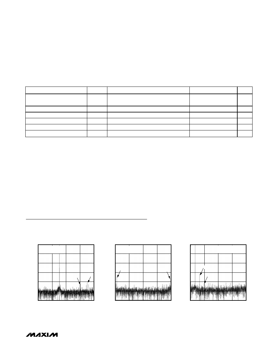
Typical Operating Characteristics
(V
AVDD
= V
DVDD
= +3.3V, AGND = DGND = 0, V
IN
= ±1.024V, differential input voltage, f
CLK
= 40MHz (50% duty cycle), digital output
load C
L
= 10pF, T
A
= T
MIN
to T
MAX,
unless otherwise noted. Typical values are at T
A
= +25°C.)
-120
-80
-100
-40
-60
-20
0
0
10
5
15
20
FFT PLOT, 4096-POINT RECORD,
DIFFERENTIAL INPUT
MAX1421 toc01
ANALOG INPUT FREQUENCY (MHz)
AMPLITUDE (dB)
f
IN
= 7.5439934MHz
A
IN
= -0.45dB FS
HD3
HD2
-120
-80
-100
-40
-60
-20
0
0
10
5
15
20
FFT PLOT, 4096-POINT RECORD,
DIFFERENTIAL INPUT
MAX1421 toc02
ANALOG INPUT FREQUENCY (MHz)
AMPLITUDE (dB)
f
IN
= 19.9047628MHz
A
IN
= -0.50dB FS
HD2
HD3
-120
-80
-100
-40
-60
-20
0
0
10
5
15
20
FFT PLOT, 4096-POINT RECORD,
DIFFERENTIAL INPUT
MAX1421 toc03
ANALOG INPUT FREQUENCY (MHz)
AMPLITUDE (dB)
f
IN
= 38.5440183MHz
A
IN
= -0.49dB FS
HD3
HD2