MAX1338 DS
General Description
The MAX1338 14-bit, analog-to-digital converter (ADC)
offers four simultaneously sampled, fully differential input
channels, with independent track-and-hold (T/H) circuitry
for each channel. The input channels are individually
software programmable for input ranges of ±10V, ±5V,
±2.5V, and ±1.25V. The input channels feature fault tol-
erance to ±17V. The internal T/H circuits have a 16ns
aperture delay and 100ps aperture-delay matching.
A 14-bit parallel bus provides the conversion result with
a maximum per-channel output rate of 150ksps
(600ksps for all four channels). The MAX1338 has an
on-board oscillator and 2.5V internal reference. An
external clock and/or reference can also be used.
The MAX1338 operates from a +5V supply for analog
inputs and digital core. The device operates from a +2.7V
to +5.25V supply for the digital I/O lines. The MAX1338
features two power-saving modes: standby mode and
shutdown mode. Standby mode allows rapid wake-up
and reduces quiescent current to 4mA (typ), and shut-
down mode reduces sleep current to less than 10µA (typ).
The MAX1338 is available in an 8mm x 8mm x 0.8mm,
56-pin, thin QFN package. The device operates over
the extended -40°C to +85°C temperature range.
Applications
Multiple-Channel Data Recorders
Vibration Analysis
Motor Control: 3-Phase Voltage, Current, and
Power Measurement
Optical Communication Equipment
Features
150ksps Sample Rate per Channel
All Four Input Channels Simultaneously Sampled
16ns Aperture Delay
100ps Aperture-Delay Matching
Channel-Independent Software-Selectable Input
Range: ±10V, ±5V, ±2.5V, ±1.25V
±17V Fault-Tolerant Inputs
Dynamic Performance at 10kHz Input
SNR: 77dB
SINAD: 76dB
SFDR: 98dBc
THD: -83dBc
DC Performance
INL: ±2 LSB
DNL: ±1 LSB
Offset Error: ±4 LSB
Gain Error: ±0.1% FSR
14-Bit Parallel Interface
Internal Clock and Reference Voltage
+5V Analog and Digital Supplies
+2.7V to +5.25V Digital I/O Supply
56-Pin Thin QFN Package (8mm x 8mm x 0.8mm)
MAX1338
14-Bit, 4-Channel, Software-Programmable,
Multiranging, Simultaneous-Sampling ADC
________________________________________________________________
Maxim Integrated Products
1
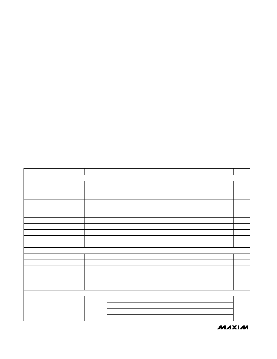
Ordering Information
19-3151; Rev 0; 4/04
For pricing, delivery, and ordering information, please contact Maxim/Dallas Direct! at
1-888-629-4642, or visit Maxim's website at www.maxim-ic.com.
PART
TEMP RANGE
PIN-PACKAGE
MAX1338ETN
-40
°
C to +85
°
C
56 Thin QFN-EP*
*EP = Exposed pad.
Pin Configuration appears at end of data sheet.
MAX1338
14-Bit, 4-Channel, Software-Programmable,
Multiranging, Simultaneous-Sampling ADC
2
_______________________________________________________________________________________
ABSOLUTE MAXIMUM RATINGS
Stresses beyond those listed under "Absolute Maximum Ratings" may cause permanent damage to the device. These are stress ratings only, and functional
operation of the device at these or any other conditions beyond those indicated in the operational sections of the specifications is not implied. Exposure to
absolute maximum rating conditions for extended periods may affect device reliability.
AV
DD
to AGND .........................................................-0.3V to +6V
DV
DD
to DGND.........................................................-0.3V to +6V
DRV
DD
to DRGND ....................................................-0.3V to +6V
AV
DD
to DV
DD
.......................................................-0.3V to +0.3V
DGND to DRGND ..................................................-0.3V to +0.3V
AGND to DGND.....................................................-0.3V to +0.3V
AGND to DRGND ..................................................-0.3V to +0.3V
AIN0+, AIN0-, AIN1+, AIN1-, AIN2+, AIN2-, AIN3+,
AIN3- to AGND .....................................................-17V to +17V
D0D13 to DRGND................................-0.3V to (DRV
DD
+ 0.3V)
REFADC, REFP1, REFP2, REFN1, REFN2, COM1, COM2 to
AGND....................................................-0.3V to (AV
DD
+ 0.3V)
INTCLK/EXTCLK to AGND.......................-0.3V to (AV
DD
+ 0.3V)
CS, RD, WR, CONVST, to DRGND........-0.3V to (DRV
DD
+ 0.3V)
SHDN, STANDBY, CLK, EOC,
EOLC to DRGND ................................-0.3V to (DRV
DD
+ 0.3V)
Maximum Current into Any Pin .........................................±50mA
Continuous Power Dissipation (T
A
= +70°C)
56-Pin Thin QFN (derate 31.3mW /°C above +70°C)....2500mW
Operating Temperature Range ...........................-40°C to +85°C
Storage Temperature Range .............................-65°C to +150°C
Maximum Junction Temperature .....................................+150°C
Lead Temperature (soldering, 10s) .................................+300°C
Junction to Ambient Thermal Resistance
JA
..................32°C/W
Junction to Case Thermal Resistance
JC
.........................2°C/W
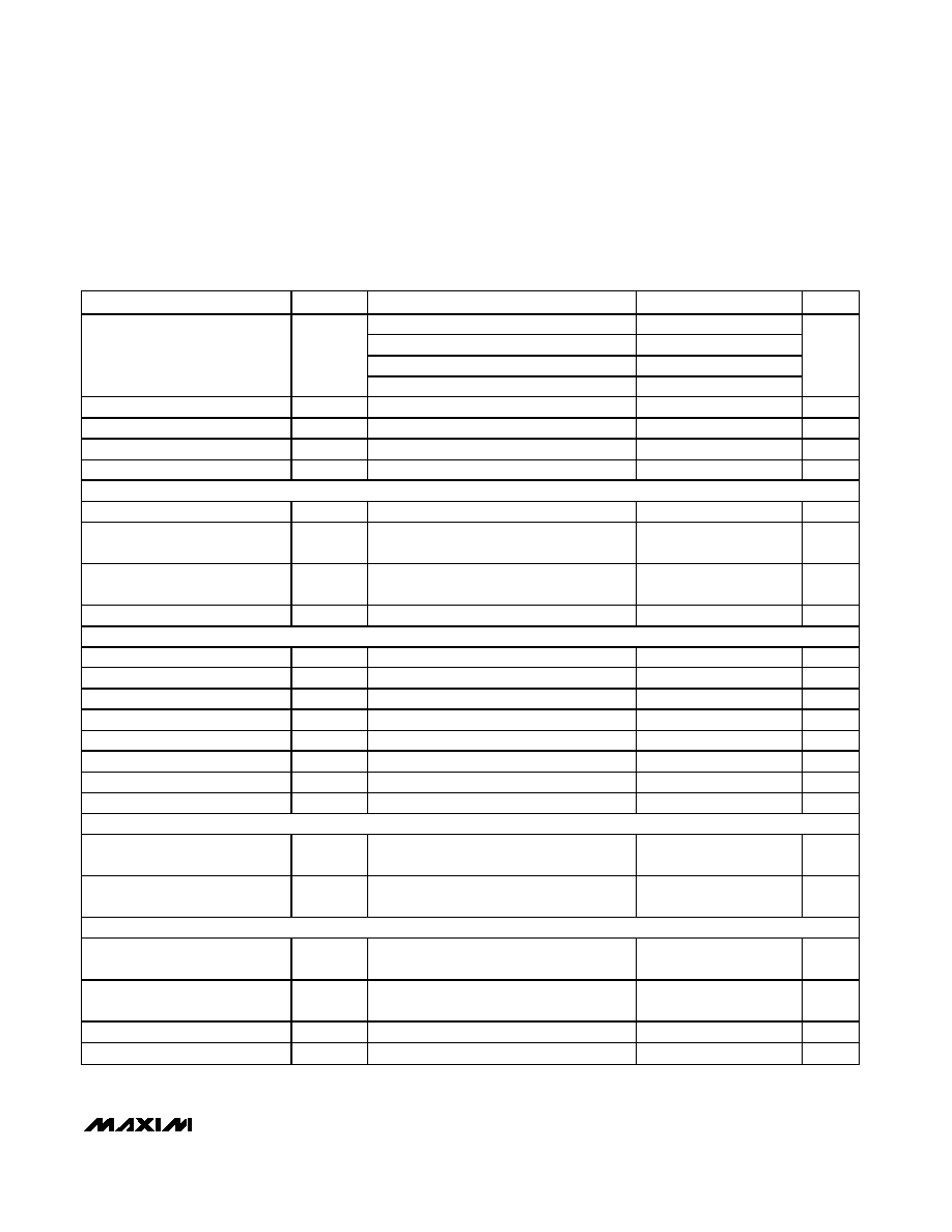
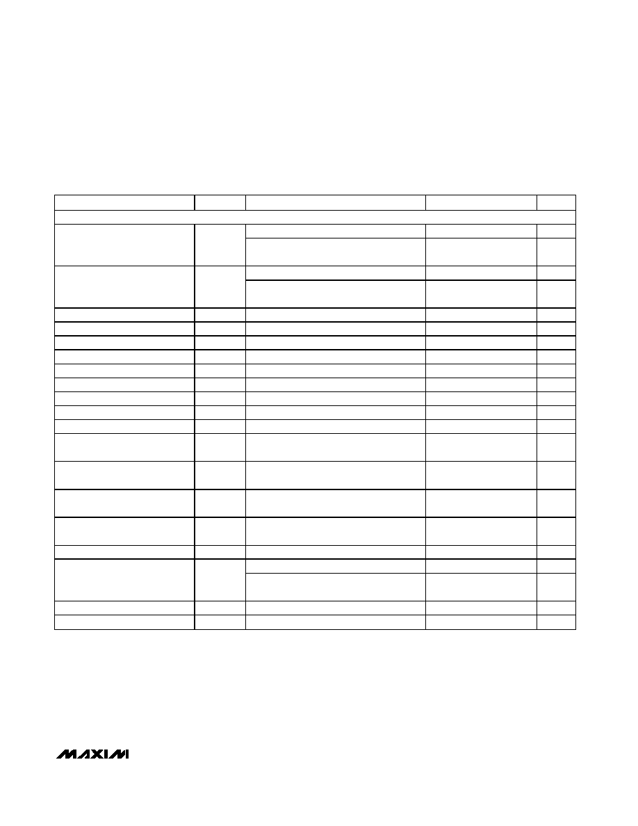
ELECTRICAL CHARACTERISTICS
(AV
DD
= DV
DD
= +5.0V, DRV
DD
= +3.0V, AGND = DGND = DRGND = 0, INTCLK/EXTCLK = AGND, f
CLK
= 5MHz, input range =
±10V, REFP2 = REFP1, REFN2 = REFN1, COM1 = COM2, 1.0nF from REFADC to AGND, 1.0µF and 0.1µF from COM1 to AGND,
0.1µF from REFP1 to AGND, 0.1µF from REFN1 to AGND, 1.0µF from REFP1 to REFN1. Typical values are at T
A
= +25°C. T
A
= T
MIN
to T
MAX
, unless otherwise noted.)
PARAMETER
SYMBOL
CONDITIONS
MIN
TYP
MAX
UNITS
STATIC PERFORMANCE
Resolution
N
14
Bits
Integral Nonlinearity
INL
(Note 1)
±
1
±
3
LSB
Differential Nonlinearity
DNL
No missing codes (Note 1)
±
0.25
±
1
LSB
Offset Error
(Note 1)
±
4
±
16
LSB
Offset-Error Temperature
Coefficient
5
ppm/°C
Offset-Error Matching
±
10
LSB
Gain Error
Offset nulled (Notes 1, 2)
±
0.1
±
0.35
%FSR
Channel Gain-Error Matching
Offset nulled
±
20
LSB
Gain-Error Temperature
Coefficient
Offset nulled
10
ppm/
°
C
DYNAMIC PERFORMANCE
(at f
IN
= 10kHz, A
IN
= -0.2dBFS)
Sampling Rate Per Channel
Simultaneous on all channels
150
ksps
Signal-to-Noise Ratio
SNR
(Note 1)
75
77
dB
Signal-to-Noise Plus Distortion
SINAD
(Note 1)
74
76
dB
Total Harmonic Distortion
THD
(Note 1)
-83
-80
dBc
Spurious-Free Dynamic Range
SFDR
Range 0 (Note 1)
85
dBc
Channel-to-Channel Isolation
(Note 1)
80
dB
ANALOG INPUTS
(AIN_)
Range set bits = (0,0)
-10
+10
Range set bits = (0,1)
-5
+5
Range set bits = (1,0)
-2.5
+2.5
Input Differential Voltage Range
Range set bits = (1,1)
-1.25
+1.25
V
MAX1338
14-Bit, 4-Channel, Software-Programmable,
Multiranging, Simultaneous-Sampling ADC
_______________________________________________________________________________________
3
ELECTRICAL CHARACTERISTICS (continued)
(AV
DD
= DV
DD
= +5.0V, DRV
DD
= +3.0V, AGND = DGND = DRGND = 0, INTCLK/EXTCLK = AGND, f
CLK
= 5MHz, input range =
±10V, REFP2 = REFP1, REFN2 = REFN1, COM1 = COM2, 1.0nF from REFADC to AGND, 1.0µF and 0.1µF from COM1 to AGND,
0.1µF from REFP1 to AGND, 0.1µF from REFN1 to AGND, 1.0µF from REFP1 to REFN1. Typical values are at T
A
= +25°C. T
A
= T
MIN
to T
MAX
, unless otherwise noted.)
PARAMETER
SYMBOL
CONDITIONS
MIN
TYP
MAX
UNITS
Range set bits = (0,0)
-5
+5
Range set bits = (0,1)
-2.5
+2.5
Range set bits = (1,0)
-1.25
+1.25
Input Common-Mode Range
Range set bits = (1,1)
-0.625
+0.625
V
Input Resistance
All settings
6.25
k
Input Capacitance
15
pF
Small-Signal Bandwidth
SSBW
(Note 1)
1
MHz
Full-Power Bandwidth
FPBW
(Note 1)
75
kHz
INTERNAL REFERENCE
(REFADC)
Output Voltage
2.475
2.5
2.525
V
Differential Reference Voltage
REFP
REFN
2.5
V
Output-Voltage Temperature
Coefficient
50
ppm/
°
C
Load Regulation
5
V/mA
EXTERNAL REFERENCE
REFADC Voltage Input Range
2.0
2.5
3.0
V
REFADC Input Current
(Note 3)
-250
+250
µA
REFADC Input Resistance
R
REF
5
k
REFADC Input Capacitance
15
pF
TRACK/HOLD (T/H)
Aperture Delay
t
AD
(Note 1)
16
ns
Aperture-Delay Matching
100
ps
Aperture Jitter
t
AJ
(Note 1)
50
ps
RMS
CLOCK-SELECT INPUT
(INTCLK/
EXTCLK
)
Input-Voltage High
V
IH
0.7 x
AV
DD
V
Input-Voltage Low
V
IL
0.3 x
AV
DD
V
DIGITAL INTERFACE AND CONTROL INPUTS
(
CS
,
RD
,
WR
, CONVST, SHDN, CLK, STANDBY)
Input-Voltage High
V
IH
0.7 x
DRV
DD
V
Input-Voltage Low
V
IL
0.3 x
DRV
DD
V
Input Hysteresis
50
mV
Input Capacitance
C
IN
15
pF
MAX1338
14-Bit, 4-Channel, Software-Programmable,
Multiranging, Simultaneous-Sampling ADC
4
_______________________________________________________________________________________
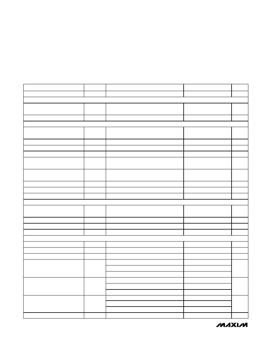
ELECTRICAL CHARACTERISTICS (continued)
(AV
DD
= DV
DD
= +5.0V, DRV
DD
= +3.0V, AGND = DGND = DRGND = 0, INTCLK/EXTCLK = AGND, f
CLK
= 5MHz, input range =
±10V, REFP2 = REFP1, REFN2 = REFN1, COM1 = COM2, 1.0nF from REFADC to AGND, 1.0µF and 0.1µF from COM1 to AGND,
0.1µF from REFP1 to AGND, 0.1µF from REFN1 to AGND, 1.0µF from REFP1 to REFN1. Typical values are at T
A
= +25°C. T
A
= T
MIN
to T
MAX
, unless otherwise noted.)
PARAMETER
SYMBOL
CONDITIONS
MIN
TYP
MAX
UNITS
Input Current
I
IN
V
IN
= 0 or DRV
DD
±1
µA
DIGITAL INTERFACE AND CONTROL OUTPUTS
(
EOC
,
EOLC
)
Output-Voltage High
V
OH
Sourcing 0.8mA
DRV
DD
- 0.6
V
Output-Voltage Low
V
OL
Sinking 1.6mA
0.4
V
PARALLEL DIGITAL I/O (D0D7)
Output-Voltage High
V
OH
Sourcing 0.8mA
DRV
DD
-
0.6
V
Output-Voltage Low
V
OL
Sinking 1.6mA
0.4
V
Leakage Current
1
µA
Tristate Output Capacitance
RD = 1 or CS = 1
15
pF
Input-Voltage High
V
IH
0.7 x
DRV
DD
V
Input-Voltage Low
V
IL
0.3 x
DRV
DD
V
Input Hysteresis
50
mV
Input Capacitance
C
IN
15
pF
Input Current
I
IN
V
IN
= 0 or DRV
DD
±1
µA
PARALLEL DIGITAL OUTPUTS (D8D13)
Output-Voltage High
V
OH
Sourcing 0.8mA
DRV
DD
-
0.6
V
Output-Voltage Low
V
OL
Sinking 1.6mA
0.4
V
Leakage Current
1
µA
Tristate Output Capacitance
15
pF
POWER SUPPLIES
Analog Supply Voltage
AV
DD
4.75
5
5.25
V
Digital Supply Voltage
DV
DD
4.75
5
5.25
V
Parallel Digital I/O Supply Voltage
DRV
DD
2.70
5.25
V
41
60
SHDN = 1
0.005
0.1
Analog Supply Current
AI
DD
STANDBY = 1, SHDN = 0
4.2
5
mA
3
SHDN = 1
0.001
0.05
Digital Supply Current
DI
DD
STANDBY = 1, SHDN = 0
0.001
0.05
mA
3
SHDN = 1
0
0.05
Digital Driver Supply Current
DRI
DD
STANDBY = 1, SHDN = 0
0
0.05
mA
Analog Power-Supply Rejection
4.75V to 5.25V (Note 1)
75
dB
MAX1338
14-Bit, 4-Channel, Software-Programmable,
Multiranging, Simultaneous-Sampling ADC
_______________________________________________________________________________________
5
ELECTRICAL CHARACTERISTICS (continued)
(AV
DD
= DV
DD
= +5.0V, DRV
DD
= +3.0V, AGND = DGND = DRGND = 0, INTCLK/EXTCLK = AGND, f
CLK
= 5MHz, input range =
±10V, REFP2 = REFP1, REFN2 = REFN1, COM1 = COM2, 1.0nF from REFADC to AGND, 1.0µF and 0.1µF from COM1 to AGND,
0.1µF from REFP1 to AGND, 0.1µF from REFN1 to AGND, 1.0µF from REFP1 to REFN1. Typical values are at T
A
= +25°C. T
A
= T
MIN
to T
MAX
, unless otherwise noted.)
PARAMETER
SYMBOL
CONDITIONS
MIN
TYP
MAX
UNITS
TIMING CHARACTERISTICS
(Figures 4, 5, and 6)
Internal clock
2.9
3.2
3.5
µs
Time to First Conversion Result
t
EOC1
External clock
16
CLK
Cycles
Internal clock
600
ns
Time to Subsequent Conversions
t
NEXT
External clock
3
CLK
Cycles
CONVST Pulse-Width Low
t
CONVST
0.1
µs
CS Pulse Width
t
CS
30
ns
RD Pulse-Width Low
t
RDL
30
ns
RD Pulse-Width High
t
RDH
30
ns
WR Pulse-Width Low
t
WRL
30
ns
CS to WR Setup Time
t
CTW
0
ns
WR to CS Hold Time
t
WTC
0
ns
CS to RD Setup Time
t
CTR
0
ns
RD to CS Hold Time
t
RTC
0
ns
Data Access Time
(RD Low to Valid Data)
t
ACC
Figure 1
30
ns
Bus Relinquish Time
(RD High to D_ High-Z)
t
REQ
Figure 1
5
30
ns
CLK Rise to End-of-Conversion
(EOC) Rise/Fall Delay
t
EOCD
20
ns
CLK Rise to End-of-Last-
Conversion (EOLC) Fall Delay
t
EOLCD
20
ns
CONVST Rise to EOLC Fall Delay
t
CVEOLCD
20
ns
Internal clock
180
200
ns
EOC Pulse-Width Low
t
EOC
External clock
1
CLK
Cycle
Wake-Up Time From Standby
7
µs
Wake-Up Time From Shutdown
All bypass capacitors discharged
5
ns