MAX1197 DS
General Description
The MAX1197 is a 3V, dual, 8-bit analog-to-digital con-
verter (ADC) featuring fully differential wideband track-
and-hold (T/H) inputs, driving two ADCs. The MAX1197
is optimized for low-power, small size, and high-dynam-
ic performance for applications in imaging, instrumenta-
tion and digital communications. This ADC operates
from a single 2.7V to 3.6V supply, consuming only
120mW while delivering a typical signal-to-noise and
distortion (SINAD) of 48.5dB at an input frequency of
30MHz and a sampling rate of 60Msps. The T/H-driven
input stages incorporate 400MHz (-3dB) input ampli-
fiers. The converters may also be operated with single-
ended inputs. In addition to low operating power, the
MAX1197 features a 3mA sleep mode as well as a
0.1µA power-down mode to conserve power during idle
periods.
An internal 2.048V precision bandgap reference sets
the full-scale range of the ADC. A flexible reference
structure allows the use of this internal or an externally
applied reference, if desired, for applications requiring
increased accuracy or a different input voltage range.
The MAX1197 features parallel, CMOS-compatible three-
state outputs. The digital output format can be set to two's
complement or straight offset binary through a single con-
trol pin. The device provides for a separate output power
supply of 1.7V to 3.6V for flexible interfacing with various
logic families. The MAX1197 is available in a 7mm x 7mm,
48-pin TQFP package, and is specified for the extended
industrial (-40°C to +85°C) temperature range.
Pin-compatible lower and higher speed versions of the
MAX1197 are also available. Refer to the MAX1195 data
sheet for 40Msps and the MAX1198 data sheet for
100Msps. In addition to these speed grades, this family
will include a multiplexed output version (MAX1196,
40Msps), for which digital data is presented time inter-
leaved and on a single, parallel 8-bit output port.
For a 10-bit, pin-compatible upgrade, refer to the
MAX1182 data sheet. With the N.C. pins of the
MAX1197 internally pulled down to ground, this ADC
becomes a drop-in replacement for the MAX1182.
Applications
Features
o Single 2.7V to 3.6V Operation
o Excellent Dynamic Performance
48.5dB/45.3dB SINAD at f
IN
= 30MHz/200MHz
69dBc/53.5dBc SFDR at f
IN
= 30MHz/200MHz
o -72dB Interchannel Crosstalk at f
IN
= 20MHz
o Low Power
120mW (Normal Operation)
9mW (Sleep Mode)
0.3µW (Shutdown Mode)
o 0.05dB Gain and ±0.05° Phase Matching
o Wide ±1V
P-P
Differential Analog Input Voltage
Range
o 400MHz -3dB Input Bandwidth
o On-Chip 2.048V Precision Bandgap Reference
o User-Selectable Output Format--Two's
Complement or Offset Binary
o Pin-Compatible 8-Bit and 10-Bit Upgrades
Available
MAX1197
Dual, 8-Bit, 60Msps, 3V, Low-Power ADC with
Internal Reference and Parallel Outputs
________________________________________________________________ Maxim Integrated Products
1
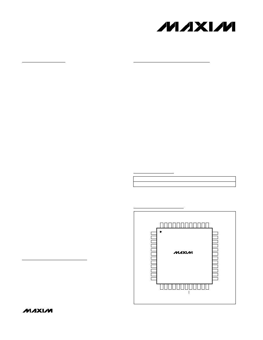
N.C.
N.C.
OGND
OV
DD
OV
DD
OGND
N.C.
N.C.
D0B
D1B
D2B
D3B
COM
V
DD
GND
INA+
INA-
V
DD
GND
INB-
INB+
GND
V
DD
CLK
1
2
3
4
5
6
7
8
9
10
11
12
36
35
34
33
32
31
30
29
28
27
26
25
TQFP-EP
GND
V
DD
GND
V
DD
T/B
SLEEP
PD
OE
D7B
D6B
D5B
D4B
13
14
15
16
17
18
19
20
21
22
23
24
48
47
46
45
44
43
42
41
40
39
38
37
REFN
REFP
REFIN
REFOUT
D7A
D6A
D5A
D4A
D3A
D2A
D1A
D0A
MAX1197
Pin Configuration
Ordering Information
19-2411; Rev 0; 4/02
For pricing, delivery, and ordering information, please contact Maxim/Dallas Direct! at
1-888-629-4642, or visit Maxim's website at www.maxim-ic.com.
Functional Diagram and Pin Compatible Upgrades table
appear at end of data sheet.
*EP = Exposed paddle
Baseband I/Q Sampling
Multichannel IF Sampling
Ultrasound and Medical
Imaging
Battery-Powered
Instrumentation
WLAN, WWAN, WLL,
MMDS Modems
Set-Top Boxes
VSAT Terminals
PART
TEMP RANGE
PIN-PACKAGE
MAX1197ECM
-40
°C to +85°C
48 TQFP-EP*
MAX1197
Dual, 8-Bit, 60Msps, 3V, Low-Power ADC with
Internal Reference and Parallel Outputs
2
_______________________________________________________________________________________
ABSOLUTE MAXIMUM RATINGS
ELECTRICAL CHARACTERISTICS
(V
DD
= OV
DD
= 3V, 0.1µF and 2.2µF capacitors from REFP, REFN, and COM to GND; REFOUT connected to REFIN through a 10k
resistor, V
IN
= 2V
P-P
(differential with respect to COM), C
L
= 10pF at digital outputs, f
CLK
= 60MHz, T
A
= T
MIN
to T
MAX
, unless otherwise
noted.
+25°C guaranteed by production test, < +25°C guaranteed by design and characterization. Typical values are at T
A
= +25
°C.)
Stresses beyond those listed under "Absolute Maximum Ratings" may cause permanent damage to the device. These are stress ratings only, and functional
operation of the device at these or any other conditions beyond those indicated in the operational sections of the specifications is not implied. Exposure to
absolute maximum rating conditions for extended periods may affect device reliability.
V
DD
, OV
DD
to GND ...............................................-0.3V to +3.6V
OGND to GND.......................................................-0.3V to +0.3V
INA+, INA-, INB+, INB- to GND ...............................-0.3V to V
DD
REFIN, REFOUT, REFP, REFN,
COM, CLK to GND .................................-0.3V to (V
DD
+ 0.3V)
OE, PD, SLEEP, T/B, D7AD0A,
D7BD0B to OGND .............................-0.3V to (OV
DD
+ 0.3V)
Continuous Power Dissipation (T
A
= +70°C)
48-Pin TQFP (derate 12.5mW/°C above +70°C).........1000mW
Operating Temperature Range ...........................-40°C to +85°C
Junction Temperature ......................................................+150°C
Storage Temperature Range .............................-60°C to +150°C
Lead Temperature (soldering, 10s) .................................+300°C
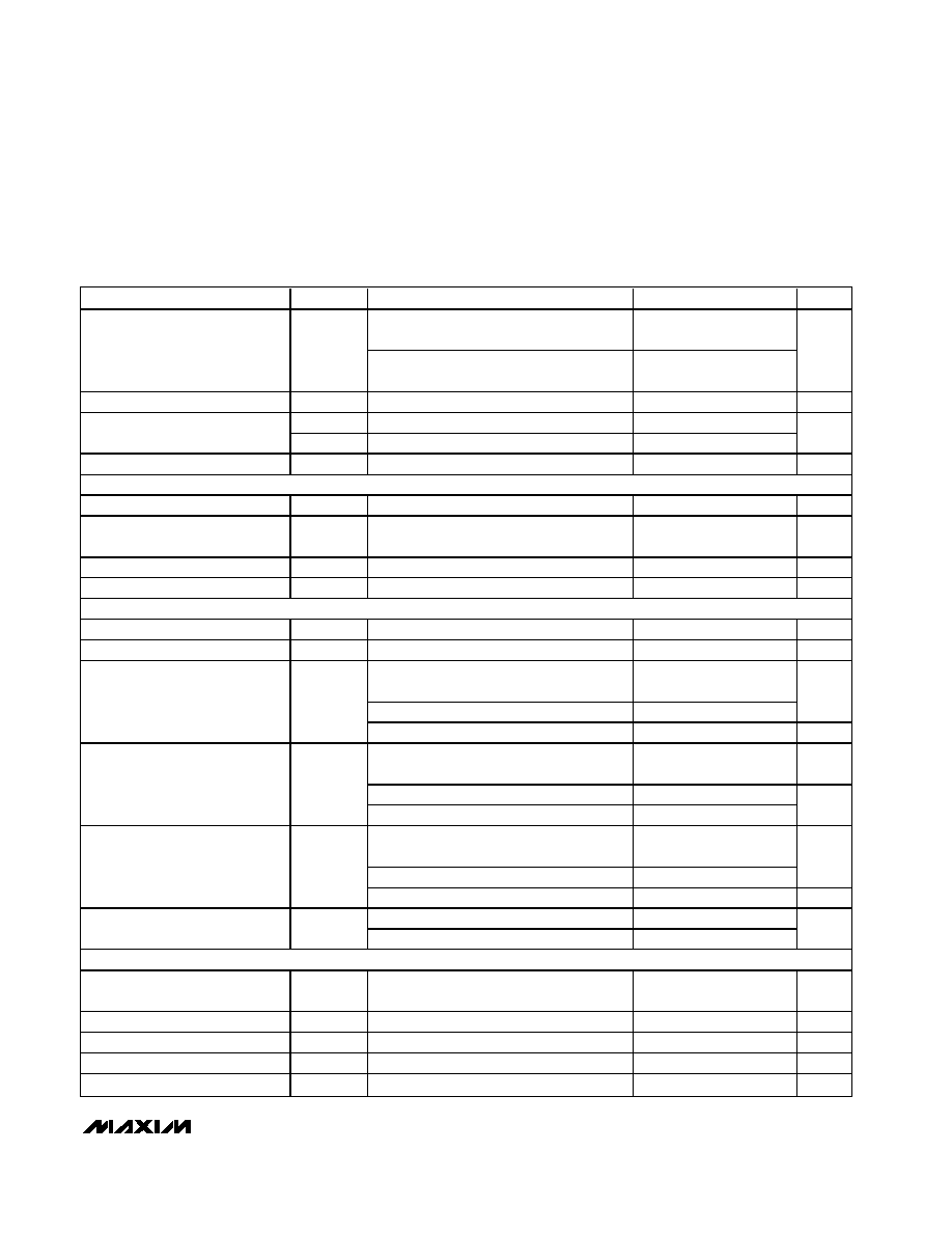
PARAMETER
SYMBOL
CONDITIONS
MIN
T YP
MAX
UNITS
DC ACCURACY
Resolution
8
Bits
Integral Nonlinearity
INL
f
IN
= 7.5MHz (Note 1)
±0.3
±1
LSB
Differential Nonlinearity
DNL
f
IN
= 7.5MHz, no missing codes guaranteed
(Note 1)
±0.2
±1
LSB
Offset Error
±4
%FS
Gain Error
±4
%FS
Gain Temperature Coefficient
±100
ppm/
°C
ANALOG INPUT
Differential Input Voltage Range
V
DIFF
Differential or single-ended inputs
±1.0
V
Common-Mode Input Voltage
Range
V
CM
V
D D
/ 2
±0.2
V
Input Resistance
R
IN
Switched capacitor load
95
k
Input Capacitance
C
IN
5
pF
CONVERSION RATE
Maximum Clock Frequency
f
CLK
60
MHz
Data Latency
5
Clock
Cycles
DYNAMIC CHARACTERISTICS (f
CLK
= 60MHz, 4096-point FFT)
f
INA or B
= 7.5MHz at -1dB FS
48.7
f
INA or B
= 20MHz at -1dB FS
47
48.7
f
INA or B
= 30MHz at -1dB FS
48.6
Signal-to-Noise Ratio
SNR
f
INA or B
= 115.1MHz at -1dB FS
48.3
dB
MAX1197
Dual, 8-Bit, 60Msps, 3V, Low-Power ADC with
Internal Reference and Parallel Outputs
_______________________________________________________________________________________
3
ELECTRICAL CHARACTERISTICS (continued)
(V
DD
= OV
DD
= 3V, 0.1µF and 2.2µF capacitors from REFP, REFN, and COM to GND; REFOUT connected to REFIN through a 10k
resistor, V
IN
= 2V
P-P
(differential with respect to COM), C
L
= 10pF at digital outputs, f
CLK
= 60MHz, T
A
= T
MIN
to T
MAX
, unless otherwise
noted.
+25°C guaranteed by production test, < +25°C guaranteed by design and characterization. Typical values are at T
A
= +25
°C.)
PARAMETER
SYMBOL
CONDITIONS
MIN
T YP
MAX
UNITS
f
INA or B
= 7.5MHz at -1dB FS
48.6
f
INA or B
= 20MHz at -1dB FS
46.5
48.6
f
INA or B
= 30MHz at -1dB FS
48.5
Signal-to-Noise
and Distortion
SINAD
f
INA or B
= 115.1MHz at -1dB FS
48.2
dB
f
INA or B
= 7.5MHz at -1dB FS
71
f
INA or B
= 20MHz at -1dB FS
60
69
f
INA or B
= 30MHz at -1dB FS
69
Spurious-Free
Dynamic Range
SFDR
f
INA or B
= 115.1MHz at -1dB FS
68
dBc
f
INA or B
= 7.5MHz at -1dB FS
- 75
f
INA or B
= 20MHz at -1dB FS
- 72
f
INA or B
= 30MHz at -1dB FS
- 72
Third-Harmonic
Distortion
HD3
f
INA or B
= 115.1MHz at -1dB FS
- 68
dBc
Intermodulation Distortion
(First Five Odd-Order IMDs)
IMD
f
IN1(A or B)
= 1.985MHz at -7dB FS
f
IN2(A or B)
= 2.029MHz at -7dB FS
(Note 2)
- 70
dBc
Third-Order Intermodulation
Distortion
IM3
f
IN1(A or B)
= 1.985MHz at -7dB FS
f
IN2(A or B)
= 2.029MHz at -7dB FS
(Note 2)
- 71.8
dBc
f
INA or B
= 7.5MHz at -1dB FS
- 69
f
INA or B
= 20MHz at -1dB FS
- 67
- 57
f
INA or B
= 30MHz at -1dB FS
- 67
Total Harmonic Distortion
(First Four Harmonics)
THD
f
INA or B
= 115.1MHz at -1dB FS
- 65
dBc
Small-Signal Bandwidth
Input at -20dB FS, differential inputs
500
MHz
Full-Power Bandwidth
FPBW
Input at -1dB FS, differential inputs
400
MHz
Gain Flatness
(12MHz Spacing)
f
IN1(A or B)
= 106 MHz at -1dB FS
f
IN2(A or B)
= 118 MHz at -1dB FS
(Note 3)
0.05
dB
Aperture Delay
t
AD
1
ns
Aperture Jitter
t
AJ
1dB SNR degradation at Nyquist
2
ps
RMS
Overdrive Recovery Time
For 1.5
× full-scale input
2
ns
IN T ER N A L REF ER EN C E ( RE FIN = RE FOU T thr oug h 10k
r esi stor ; RE FP , RE FN , and C OM l evel s ar e g ener ated i nter nal l y.)
Reference Output Voltage
V
REFOUT
(Note 4)
2.048
± 3%
V
Positive Reference Output
Voltage
V
REFP
(Note 5)
2.012
V
Negative Reference Output
Voltage
V
REFN
(Note 5)
0.988
V
Common-Mode Level
V
COM
(Note 5)
V
D D
/ 2
±0.1
V
MAX1197
Dual, 8-Bit, 60Msps, 3V, Low-Power ADC with
Internal Reference and Parallel Outputs
4
_______________________________________________________________________________________
ELECTRICAL CHARACTERISTICS (continued)
(V
DD
= OV
DD
= 3V, 0.1µF and 2.2µF capacitors from REFP, REFN, and COM to GND; REFOUT connected to REFIN through a 10k
resistor, V
IN
= 2V
P-P
(differential with respect to COM), C
L
= 10pF at digital outputs, f
CLK
= 60MHz, T
A
= T
MIN
to T
MAX
, unless otherwise
noted.
+25°C guaranteed by production test, < +25°C guaranteed by design and characterization. Typical values are at T
A
= +25
°C.)
PARAMETER
SYMBOL
CONDITIONS
MIN
T YP
MAX
UNITS
Differential Reference Output
Voltage Range
V
REF
V
REF
= V
REFP
- V
REFN
1.024
± 3%
V
Reference Temperature
Coefficient
TC
REF
±100
ppm/°C
BUFFERED EXTERNAL REFERENCE (V
REFIN
= 2.048V)
Positive Reference Output
Voltage
V
REFP
(Note 5)
2.012
V
Negative Reference Output
Voltage
V
REFN
(Note 5)
0.988
V
Common-Mode Level
V
COM
(Note 5)
V
D D
/ 2
± 0.1
V
Differential Reference Output
Voltage Range
V
REF
V
REF
= V
REFP
- V
REFN
1.024
± 2%
V
REFIN Resistance
R
REFIN
750
M
Maximum REFP, COM Source
Current
I
SOURCE
5
mA
Maximum REFP, COM Sink
Current
I
SINK
- 250
µA
Maximum REFN Source Current
I
SOURCE
250
µA
Maximum REFN Sink Current
I
SINK
- 5
mA
U N B U F F ER ED EXT ER N A L R EF ER EN C E ( V
RE F IN
= AGN D , r efer ence vol tag e ap p l i ed to RE FP , RE FN , and C OM )
REFP, REFN Input Resistance
R
REFP
,
R
REFN
Measured between REFP, COM, REFN,
and COM
4
k
REFP, REFN, COM Input
Capacitance
C
IN
15
pF
Differential Reference Input
Voltage Range
V
REF
V
REF
= V
REFP
- V
REFN
1.024
±10%
V
COM Input Voltage Range
V
COM
V
D D
/ 2
±5%
V
REFP Input Voltage
V
REFP
V
C OM
+
V
RE F
/ 2
V
REFN Input Voltage
V
REFN
V
C OM
-
V
RE F
/ 2
V
DIGITAL INPUTS (CLK, PD,
OE, SLEEP, T/B)
CLK
0.8
×
V
DD
Input High Threshold
V
IH
PD,
OE, SLEEP, T/B
0.8
×
OV
DD
V
MAX1197
Dual, 8-Bit, 60Msps, 3V, Low-Power ADC with
Internal Reference and Parallel Outputs
_______________________________________________________________________________________
5
ELECTRICAL CHARACTERISTICS (continued)
(V
DD
= OV
DD
= 3V, 0.1µF and 2.2µF capacitors from REFP, REFN, and COM to GND; REFOUT connected to REFIN through a 10k
resistor, V
IN
= 2V
P-P
(differential with respect to COM), C
L
= 10pF at digital outputs, f
CLK
= 60MHz, T
A
= T
MIN
to T
MAX
, unless otherwise
noted.
+25°C guaranteed by production test, < +25°C guaranteed by design and characterization. Typical values are at T
A
= +25
°C.)
PARAMETER
SYMBOL
CONDITIONS
MIN
T YP
MAX
UNITS
CLK
0.2
×
V
DD
Input Low Threshold
V
IL
PD,
OE, SLEEP, T/B
0.2
×
OV
DD
V
Input Hysteresis
V
HYST
0.15
V
I
IH
V
IH
= V
DD
= OV
DD
±20
Input Leakage
I
IL
V
IL
= 0
±20
µA
Input Capacitance
C
IN
5
pF
DIGITAL OUTPUTS (D7AD0A, D7BD0B)
Output Voltage Low
V
OL
I
SINK
= -200
µA
0.2
V
Output Voltage High
V
OH
I
SOURCE
= 200
µA
OV
DD
- 0.2
V
Three-State Leakage Current
I
LEAK
OE = OV
DD
±10
µA
Three-State Output Capacitance
C
OUT
OE = OV
DD
5
pF
POWER REQUIREMENTS
Analog Supply Voltage Range
V
DD
2.7
3
3.6
V
Output Supply Voltage Range
OV
DD
C
L
= 15pF
1.7
3
3.6
V
Operating, f
INA & B
= 20MHz at
-1dB FS applied to both channels
40
50
Sleep mode
3
mA
Analog Supply Current
I
VDD
Shutdown, clock idle, PD =
OE = OV
DD
0.1
20
µA
Operating, f
INA & B
= 20MHz at
-1dB FS applied to both channels (Note 6)
9
mA
Sleep mode
3
Output Supply Current
I
OVDD
Shutdown, clock idle, PD =
OE = OV
DD
3
10
µA
Operating, f
INA & B
= 20MHz at
-1dB FS applied to both channels
120
150
Sleep mode
9
mW
Analog Power Dissipation
PDISS
Shutdown, clock idle, PD =
OE = OV
DD
0.3
60
µW
Offset, V
DD
±5%
±3
Power-Supply
Rejection
PSRR
Gain, V
DD
±5%
±3
mV/V
TIMING CHARACTERISTICS
CLK Rise to Output Data Valid
Time
t
DO
C
L
= 20pF (Notes 1, 7)
6
9
ns
OE Fall to Output Enable Time
t
ENABLE
5
ns
OE Rise to Output Disable Time
t
DISABLE
5
ns
CLK Pulse Width High
t
CH
Clock period: 16.67ns (Note 7)
8.33 ± 1.5
ns
CLK Pulse Width Low
t
CL
Clock period: 16.67ns (Note 7)
8.33 ± 1.5
ns