_______________General Description
The MAX1160 10-bit, monolithic analog-to-digital con-
verter (ADC) is capable of 20Msps minimum word
rates. An on-board track/hold ensures excellent dynam-
ic performance without the need for external compo-
nents. A 5pF input capacitance minimizes drive
requirement problems.
Inputs and outputs are TTL compatible. An overrange
output is provided to indicate overflow conditions. Output
data format is straight binary. Power dissipation is low at
only 1W with +5V and -5.2V power-supply voltages. The
MAX1160 also accepts wide Ý2V input voltages.
The MAX1160 is available in 28-pin DIP and SO pack-
ages in the commercial temperature range.
________________________Applications
Medical Imaging
Professional Video
Radar Receivers
Instrumentation
Digital Communications
____________________________Features
o
Monolithic 20Msps Converter
o
On-Chip Track/Hold
o
Bipolar, Ý2V Analog Input
o
60dB SNR at 1MHz Input
o
5pF Input Capacitance
o
TTL Outputs
MAX1160
10-Bit, 20Msps, TTL-Output ADC
________________________________________________________________
Maxim Integrated Products
1
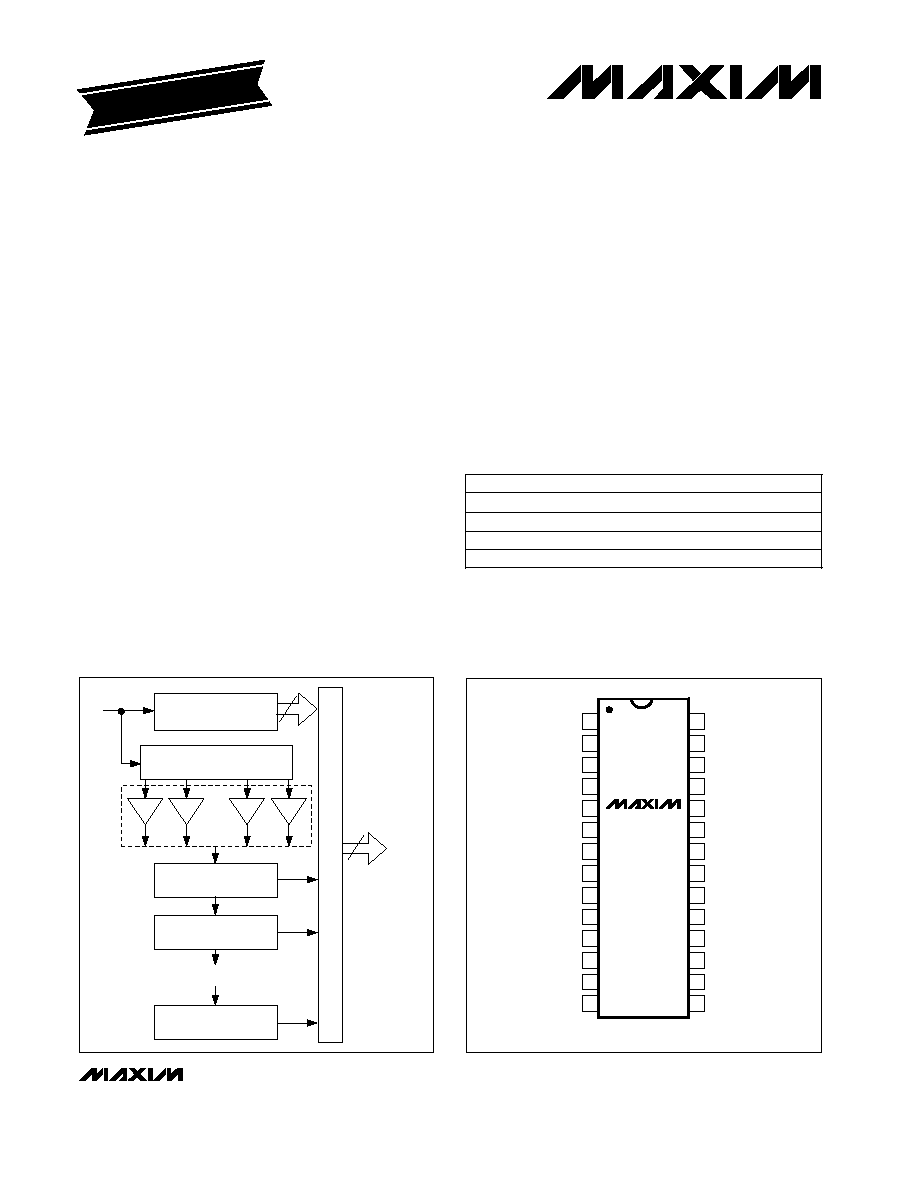
COARSE
ADC
T/H
AMPLIFIER
BANK
SUCCESSIVE INTERPOLATION
STAGE i
SUCCESSIVE INTERPOLATION
STAGE i + 1
SUCCESSIVE INTERPOLATION
STAGE N
ANALOG
PRESCALER
ANALOG
INPUT
4
10
DIGITAL
OUTPUT
DECODING NETWORK
.
.
.
.
________________Functional Diagram
19-1189; Rev 0; 3/97
For the latest literature: http://www.maxim-ic.com, or phone 1-800-998-8800
PART
MAX1160ACPI
MAX1160BCPI
MAX1160ACWI
0¯C to +70¯C
0¯C to +70¯C
0¯C to +70¯C
TEMP. RANGE
PIN-PACKAGE
28 Wide Plastic DIP
28 Wide Plastic DIP
28 SO
MAX1160BCWI
0¯C to +70¯C
28 SO
______________Ordering Information
EVALUATION KIT
AVAILABLE
__________________Pin Configuration
28
27
26
25
24
23
22
21
20
19
18
17
16
15
1
2
3
4
5
6
7
8
9
10
11
12
13
14
DIP/SO
DV
CC
V
EE
AGND
V
CC
VFB
VSB
VRM
VIN
VST
VFT
V
CC
AGND
V
EE
CLK
DGND
D0
D1
D2
D3
D4
D5
D6
D7
D8
D9
D10
DGND
DV
CC
MAX1160
TOP VIEW
TOP VIEW
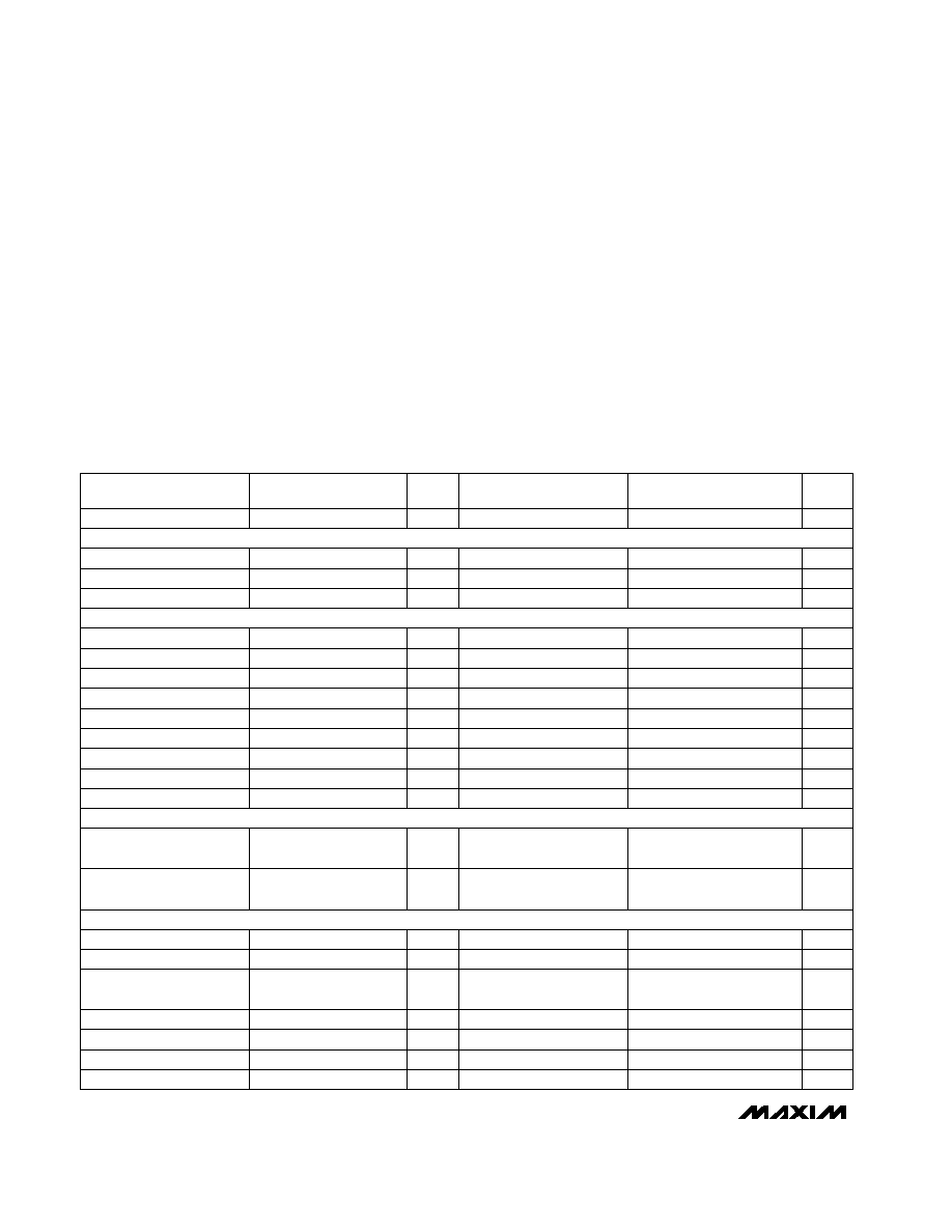
MAX1160
10-Bit, 20Msps, TTL-Output ADC
2
_______________________________________________________________________________________
ABSOLUTE MAXIMUM RATINGS
ELECTRICAL CHARACTERISTICS
(V
CC
= +5.0V, V
EE
= -5.2V, DV
CC
= +5.0V, V
IN
= Ý2.0V, VSB = -2.0V, VST = +2.0V, f
CLK
= 20MHz, 50% clock duty cycle,
T
A
= T
MIN
to T
MAX
, unless otherwise noted.)
Stresses beyond those listed under "Absolute Maximum Ratings" may cause permanent damage to the device. These are stress ratings only, and functional
operation of the device at these or any other conditions beyond those indicated in the operational sections of the specifications is not implied. Exposure to
absolute maximum rating conditions for extended periods may affect device reliability.
V
CC ..........................................................................................................
6V
V
EE .........................................................................................................
-6V
Analog Input ......................................................VFB
VIN
VFT
VFT, VFB ...........................................................................3V, -3V
Reference-Ladder Current..................................................12mA
CLK Input...............................................................................V
CC
Digital Outputs.....................................................30mA to -30mA
Continuous Power Dissipation (T
A
= +70¯C)
Plastic DIP ......................................................................1.14W
SO .......................................................................................1W
Operating Temperature Range...............................0¯C to +70¯C
Junction Temperature .....................................................+150¯C
Storage Temperature Range .............................-65¯C to +150¯C
Lead Temperature (soldering, 10sec). ............................+300¯C
V
V
V
I
VI
V
I
VI
V
VI
VI
VI
V
VI
VI
V
VI
TEST
LEVEL
ns
20
T
A
= +25¯C
Acquisition Time
ps-RMS
5
T
A
= +25¯C
Aperture Jitter Time
ns
14
18
T
A
= +25¯C
Output Delay
Clock
Cycle
1
Pipeline Delay (Latency)
ns
20
Overvoltage Recovery Time
MHz
20
Maximum Conversion Rate
/¯C
0.8
Reference-Ladder
Tempco
500
800
Reference-Ladder
Resistance
MHz
120
3dB small signal
Input Bandwidth
pF
5
Input Capacitance
k
75
300
T
A
= -55¯C to +125¯C
Input Resistance
LSB
Ý0.5
Differential Nonlinearity
LSB
Ý1.0
Bits
10
Resolution
Integral Nonlinearity
k
100
300
Input Resistance
çA
75
T
A
= -55¯C to +125¯C
Input Bias Current
çA
30
60
V
IN
= 0V
Input Bias Current
V
Ý2.0
Input Voltage Range
Guaranteed
No Missing Codes
UNITS
MAX1160A
MIN
TYP
MAX
CONDITIONS
PARAMETER
20
5
14
18
1
20
20
0.8
500
800
120
5
75
300
Ý0.75
Ý1.5
10
100
300
75
30
60
Ý2.0
Guaranteed
MAX1160B
MIN
TYP
MAX
V
LSB
Ý2.0
Positive Full-Scale Error
Ý2.0
V
LSB
Ý2.0
Negative Full-Scale Error
Ý2.0
V
ns
1
T
A
= +25¯C
Aperture Delay Time
1
DC ACCURACY
(Ý full scale, 250kHz sample rate, T
A
= +25¯C)
ANALOG INPUT
REFERENCE INPUT
TIMING CHARACTERISTICS
MAX1160
10-Bit, 20Msps, TTL-Output ADC
_______________________________________________________________________________________
3
ELECTRICAL CHARACTERISTICS (continued)
(V
CC
= +5.0V, V
EE
= -5.2V, DV
CC
= +5.0V, V
IN
= Ý2.0V, VSB = -2.0V, VST = +2.0V, f
CLK
= 20MHz, 50% clock duty cycle,
T
A
= T
MIN
to T
MAX
, unless otherwise noted.)
T
A
= +25¯C
T
A
= 0¯C to +70¯C,
T
A
= -25¯C to +85¯C
f
IN
= 1MHz
54
57
52
55
55
58
IV
57
60
I
f
IN
= 10MHz
f
IN
= 3.58MHz
f
IN
= 1MHz
MAX1160B
MIN
TYP
MAX
8.7
8.3
7.0
Effective Number of Bits
(ENOB)
7.5
Bits
PARAMETER
CONDITIONS
MAX1160A
MIN
TYP
MAX
UNITS
9.2
8.8
TEST
LEVEL
T
A
= +25¯C
T
A
= 0¯C to +70¯C,
T
A
= -25¯C to +85¯C
f
IN
= 3.58MHz
53
55
51
53
54
56
IV
56
58
I
T
A
= +25¯C
T
A
= 0¯C to +70¯C,
T
A
= -25¯C to +85¯C
f
IN
= 10MHz
47
49
44
46
Signal-to-Noise Ratio
(without harmonics)
(SNR)
47
50
dB
IV
50
53
I
T
A
= +25¯C
T
A
= 0¯C to +70¯C,
T
A
= -25¯C to +85¯C
f
IN
= 1MHz
54
57
51
54
54
57
IV
57
60
I
T
A
= +25¯C
T
A
= 0¯C to +70¯C,
T
A
= -25¯C to +85¯C
f
IN
= 3.58MHz
53
55
50
52
53
55
IV
56
58
I
T
A
= +25¯C
T
A
= 0¯C to +70¯C,
T
A
= -25¯C to +85¯C
f
IN
= 10MHz
43
45
42
44
Total Harmonic Distortion
(THD)
45
47
dB
IV
46
48
I
T
A
= +25¯C
T
A
= 0¯C to +70¯C,
T
A
= -25¯C to +85¯C
f
IN
= 1MHz
52
54
49
52
IV
55
57
I
T
A
= +25¯C
T
A
= 0¯C to +70¯C,
T
A
= -25¯C to +85¯C
f
IN
= 3.58MHz
51
52
48
51
IV
54
55
I
T
A
= +25¯C
T
A
= 0¯C to +70¯C,
T
A
= -25¯C to +85¯C
f
IN
= 10MHz
41
44
40
Signal-to-Noise and
Distortion Ratio
(SINAD)
43
IV
44
47
I
f
IN
= 1MHz
67
67
V
dB
Spurious-Free
Dynamic Range (SFDR)
f
IN
= 3.58MHz
and 4.35MHz
0.5
V
0.7
%
Differential Gain
dB
T
A
= +25¯C
T
A
= +25¯C
f
IN
= 3.58MHz
and 4.35MHz
0.2
V
0.2
Degrees
Differential Phase
T
A
= +25¯C
DYNAMIC PERFORMANCE
MAX1160
10-Bit, 20Msps, TTL-Output ADC
4
_______________________________________________________________________________________
ELECTRICAL CHARACTERISTICS (continued)
(V
CC
= +5.0V, V
EE
= -5.2V, DV
CC
= +5.0V, V
IN
= Ý2.0V, VSB = -2.0V, VST = +2.0V, f
CLK
= 20MHz, 50% clock duty cycle,
T
A
= T
MIN
to T
MAX
, unless otherwise noted.)
V
V
2.4
4.5
Logic 1 Voltage
2.4
4.0
IV
çA
0
5
20
T
A
= +25¯C
Maximum Input
Current Low
0
5
20
V
V
0.8
Logic 0 Voltage
0.8
Pulse Width High (CLK)
ns
20
300
IV
20
300
Maximum Input
Current High
Pulse Width Low (CLK)
çA
ns
20
IV
20
IV
0
5
20
0
5
20
T
A
= +25¯C
TEST
LEVEL
UNITS
MAX1160A
MIN
TYP
MAX
CONDITIONS
PARAMETER
MAX1160B
MIN
TYP
MAX
Logic 1 Voltage
V
2.4
IV
2.4
Logic 0 Voltage
V
0.6
IV
0.6
4.75
5.0
5.25
IV
4.75
5.0
5.25
DV
CC
4.75
5.25
IV
4.75
5.25
V
CC
Power Dissipation
1.0
1.3
VI
1.0
1.3
-4.95 -5.2
-5.45
IV
-4.95 -5.2
-5.45
-V
EE
Power-Supply Rejection
V
1.0
V
1.0
V
CC
= 5V Ý0.25V, V
EE
= -5.2V Ý0.25V
LSB
W
40
55
VI
40
55
DI
CC
118
145
VI
118
145
I
CC
40
57
VI
40
57
-I
EE
mA
DIGITAL INPUTS
DIGITAL OUTPUTS
POWER-SUPPLY REQUIREMENTS
Currents
Voltages
TEST LEVEL CODES
All electrical characteristics are subject to the following conditions:
All parameters having min/max specifications are guaranteed. The
Test Level column indicates the specific device testing actually per-
formed during production and Quality Assurance inspection. Any
blank section in the data column indicates that the specification is
not tested at the specified condition.
Unless otherwise noted, all tests are pulsed; therefore,
Tj = TC = TA.
TEST LEVEL
I
II
III
IV
V
VI
TEST PROCEDURE
100% production tested at the specified temperature.
100% production tested at TA = +25¯C, and sample tested at the specified
temperatures.
QA sample tested only at the specified temperatures.
Parameter is guaranteed (but not tested) by design and characterization data.
Parameter is a typical value for information purposes only.
100% production tested at TA = +25¯C. Parameter is guaranteed over specified
temperature range.
______________________________________________________________Pin Description
NAME
1, 13
DGND
2
D0
PIN
12
D10
15
CLK
3Ù10
FUNCTION
16, 27
V
EE
Digital Ground
D1ÙD8
TTL Output (LSB)
TTL Outputs
11
D9
TTL Output (MSB)
14, 28
DV
CC
+5V Supply (digital)
TTL Output Overrange
Clock
-5.2V Supply (analog)
NAME
20
VST
19
PIN
VFT
21
18, 25
V
CC
VIN
FUNCTION
22
17, 26
AGND
VRM
23
VSB
Sense for Top of Reference Ladder
24
VFB
Force for Top of Reference Ladder
+5V Supply (analog)
Analog Input
Analog Ground
Middle of Voltage Reference Ladder
Sense for Bottom of Reference Ladder
Force for Bottom of Reference Ladder

MAX1160
10-Bit, 20Msps, TTL-Output ADC
_______________________________________________________________________________________
5
80
20
1
10
100
SIGNAL-TO-NOISE RATIO vs.
INPUT FREQUENCY
40
30
MAX1160-01
INPUT FREQUENCY (MHz)
SNR (dB)
60
50
70
f
S
= 20Msps
80
20
1
10
100
SIGNAL-TO-NOISE AND DISTORTION
vs. INPUT FREQUENCY
40
30
MAX1160-03
INPUT FREQUENCY (MHz)
SINAD (dB)
60
50
70
f
S
= 20Msps
0
-120
0
7
10
8
9
1
2
3
4
5
6
SPECTRAL RESPONSE
-60
-90
MAX1160-05
INPUT FREQUENCY (MHz)
AMPLITUDE (dB)
-30
f
S
= 20Msps
f
IN
= 1MHz
80
20
1
10
100
SNR, THD, SINAD vs.
SAMPLE RATE
40
30
MAX1160-04
SAMPLE RATE (Msps)
SNR, THD, SINAD (dB)
60
50
70
SINAD
SNR, THD
f
IN
= 1MHz
65
40
-25
50
75
0
25
SNR, THD, SINAD vs.
TEMPERATURE
50
45
MAX1160-06
TEMPERATURE (¯C)
SNR, THD, SINAD (dB)
60
55
SINAD
SNR
f
S
= 20Msps
f
IN
= 1MHz
THD
THD
SNR
__________________________________________Typical Operating Characteristics
(T
A
= +25¯C, unless otherwise noted.)
80
20
1
10
100
TOTAL HARMONIC DISTORTION vs.
INPUT FREQUENCY
40
30
MAX1160-02
INPUT FREQUENCY (MHz)
THD (dB)
60
50
70
f
S
= 20Msps
______________Detailed Description
The MAX1160 requires few external components to
achieve the stated operation and performance. Figure
2 shows the typical interface requirements when using
the MAX1160 in normal circuit operation. The following
section provides a description of the pin functions, and
outlines critical performance criteria to consider for
achieving the optimal device performance.
Power Supplies and Grounding
The MAX1160 requires -5.2V and +5V analog supply
voltages. The +5V supply is common to analog V
CC
and digital DV
CC
. A ferrite bead in series with each
supply line reduces the transient noise injected into the
analog V
CC
. Connect these beads as close to the
device as possible. The connection between the beads
and the MAX1160 should not be shared with any other
device. Bypass each power-supply pin as close to the
device as possible. Use 0.1çF for V
EE
and V
CC
, and
0.01çF for DV
CC
(chip capacitors are recommended).