General Description
The DS3234 is a low-cost, extremely accurate SPITM bus
real-time clock (RTC) with an integrated temperature-
compensated crystal oscillator (TCXO) and crystal. The
DS3234 incorporates a precision, temperature-compen-
sated voltage reference and comparator circuit to moni-
tor V
CC
. When V
CC
drops below the power-fail voltage
(V
PF
), the device asserts the RST output and also dis-
ables read and write access to the part when V
CC
drops
below both V
PF
and V
BAT
. The RST pin is monitored as
a pushbutton input for generating a reset externally. The
device switches to the backup supply input and main-
tains accurate timekeeping when main power to the
device is interrupted. The integration of the crystal res-
onator enhances the long-term accuracy of the device
as well as reduces the piece-part count in a manufactur-
ing line. The DS3234 is available in commercial and
industrial temperature ranges, and is offered in an
industry-standard 300-mil, 20-pin SO package.
The DS3234 also integrates 256 bytes of battery-backed
SRAM. In the event of main power loss, the contents of
the memory are maintained by the power source con-
nected to the V
BAT
pin. The RTC maintains seconds,
minutes, hours, day, date, month, and year information.
The date at the end of the month is automatically adjust-
ed for months with fewer than 31 days, including correc-
tions for leap year. The clock operates in either the
24-hour or 12-hour format with AM/PM indicator. Two
programmable time-of-day alarms and a programmable
square-wave output are provided. Address and data are
transferred serially by an SPI bidirectional bus.
Applications
Servers
Utility Power Meters
Telematics
GPS
Features
Accuracy ±2ppm from 0°C to +40°C
Accuracy ±3.5ppm from -40°C to +85°C
Battery Backup Input for Continuous
Timekeeping
Operating Temperature Ranges
Commercial: 0°C to +70°C
Industrial: -40°C to +85°C
Low-Power Consumption
Real-Time Clock Counts Seconds, Minutes,
Hours, Day, Date, Month, and Year with Leap Year
Compensation Valid Up to 2099
Two Time-of-Day Alarms
Programmable Square-Wave Output
4MHz SPI Bus Supports Modes 1 and 3
Digital Temp Sensor Output: ±3°C Accuracy
Register for Aging Trim
RST Input/Output
300-Mil, 20-Pin SO Package
Underwriters Laboratory (UL) Recognized
DS3234
Extremely Accurate SPI Bus RTC with
Integrated Crystal and SRAM
______________________________________________ Maxim Integrated Products
1
Rev 0; 2/06
For pricing, delivery, and ordering information, please contact Maxim/Dallas Direct! at
1-888-629-4642, or visit Maxim's website at www.maxim-ic.com.
Ordering Information
PART
TEMP RANGE
PIN-
PACKAGE
TOP
MARK
DS3234S#
0°C to +70°C
20 SO
DS3234S
DS3234SN#
-40°C to +85°C
20 SO
DS3234SN
SPI is a trademark of Motorola, Inc.
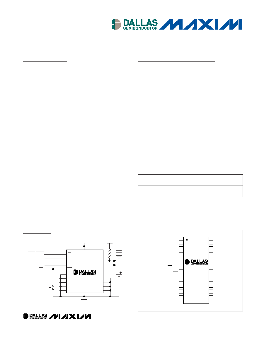
DS3234
CS
INT/SQW
32kHz
V
BAT
PUSH-
BUTTON
RESET
SCLK
RST
N.C.
N.C.
N.C.
V
CC
V
PU
V
CC
GND
V
CC
CPU
SS
SCLK
DIN
MOSI
DOUT
MISO
RST
N.C.
N.C.
N.C.
N.C.
N.C.
N.C.
Typical Operating Circuit
# Denotes a RoHS-compliant device that may include lead that
is exempt under the RoHS requirements. Lead finish is JESD97
Category e3, and is compatible with both lead-based and
lead-free soldering processes. A "#" anywhere on the top mark
denotes a RoHS-compliant device.
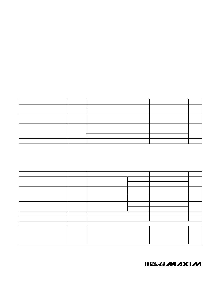
TOP VIEW
20
19
18
17
16
15
14
13
1
2
3
4
5
6
7
8
SCLK
DOUT
SCLK
DIN
V
CC
32kHz
N.C.
CS
V
BAT
GND
N.C.
N.C.
N.C.
N.C.
RST
INT/SQW
12
11
9
10
N.C.
N.C.
N.C.
N.C.
SO
DS3234
Pin Configuration
DS3234
Extremely Accurate SPI Bus RTC with
Integrated Crystal and SRAM
2
_____________________________________________________________________
ABSOLUTE MAXIMUM RATINGS
RECOMMENDED DC OPERATING CONDITIONS
(T
A
= -40°C to +85°C, unless otherwise noted.) (Notes 1, 2)
Stresses beyond those listed under "Absolute Maximum Ratings" may cause permanent damage to the device. These are stress ratings only, and functional
operation of the device at these or any other conditions beyond those indicated in the operational sections of the specifications is not implied. Exposure to
absolute maximum rating conditions for extended periods may affect device reliability.
Voltage Range on Any Pin Relative to Ground......-0.3V to +6.0V
Operating Temperature Range
(noncondensing) .............................................-40°C to +85°C
Junction Temperature ......................................................+125°C
Storage Temperature Range ...............................-40°C to +85°C
Soldering Temperature
(leads, 10s) ...........................................................+260°C/10s
Soldering Temperature (reflow, 2 times max) .......See IPC/JEDEC
J-STD-020 Specification
PARAMETER
SYMBOL
CONDITIONS
MIN
TYP
MAX
UNITS
V
CC
2.0
3.3
5.5
Supply Voltage
V
BAT
2.0
3.0
3.8
V
Logic 1 Input CS, SCLK, DIN
V
IH
0.7 x
V
CC
V
CC
+
0.3
V
2.0V V
CC
3.63V
-0.3
+0.2 x
V
CC
Logic 0 Input CS, SCLK, DIN,
RST
V
IL
3.63V < V
CC
5.5V
-0.3
+0.7
V
Pullup Voltage INT/SQW
V
PU
V
CC
= 0V
5.5
V
ELECTRICAL CHARACTERISTICS
(V
CC
= 2.0V to 5.5V, V
CC
= active supply (see Table 1), T
A
= -40°C to +85°C, unless otherwise noted.) (Typical values are at
V
CC
=
3.3V, V
BAT
= 3.0V, and T
A
= +25°C, unless otherwise noted. TCXO operation guaranteed from 2.3V to 5.5V on V
CC
and 2.3V to 3.8V on
V
BAT
.) (Notes 1, 2)
PARAMETER
SYMBOL
CONDITIONS
MIN
TYP
MAX
UNITS
V
CC
= 3.63V
400
Active Supply Current
I
CCA
SCLK = 4MHz, BSY = 0
(Notes 3, 4)
V
CC
= 5.5V
700
µA
V
CC
= 3.63V
120
Standby Supply Current
I
CCS
CS = V
IH
, 32kHz output off,
SQW output off
(Note 4)
V
CC
= 5.5V
160
µA
V
CC
= 3.63V
500
Temperature Conversion Current
I
CCSCONV
SPI bus inactive, 32kHz
output off, SQW output off
V
CC
= 5.5V
600
µA
Power-Fail Voltage
V
PF
2.45
2.575
2.70
V
V
BAT
Leakage Current
I
BATLKG
25
100
nA
(V
CC
= 2.0V to 5.5V, T
A
= -40°C to +85°C, unless otherwise noted.) (Notes 1 and 2)
Logic 1 Output, 32kHz
I
OH
= -500µA
I
OH
= -250µA
I
OH
= -125µA
V
OH
V
CC
> 3.63V,
3.63V > V
CC
> 2.7V,
2.7V > (V
CC
or V
BAT)
> 2.0V
(BB32kHz = 1)
0.85 x V
CC
V

DS3234
Extremely Accurate SPI Bus RTC with
Integrated Crystal and SRAM
_____________________________________________________________________
3
ELECTRICAL CHARACTERISTICS (continued)
(V
CC
= 2.0V to 5.5V, V
CC
= active supply (see Table 1), T
A
= -40°C to +85°C, unless otherwise noted.) (Typical values are at
V
CC
=
3.3V, V
BAT
= 3.0V, and T
A
= +25°C, unless otherwise noted. TCXO operation guaranteed from 2.3V to 5.5V on V
CC
and 2.3V to 3.8V on
V
BAT
.) (Notes 1, 2)
PARAMETER
SYMBOL
CONDITIONS
MIN
TYP
MAX
UNITS
Logic 0 Output, 32kHz
V
OL
I
OL
= 1mA
0.4
V
Logic 1 Output, DOUT
V
OH
I
OH
= -1.0mA
0.85 x V
CC
V
Logic 0 Output, DOUT, INT/SQW
V
OL
I
OL
= 3mA
0.4
V
Logic 0 Output, RST
V
OL
I
OL
= 1.0mA
0.4
V
Output Leakage Current 32kHz,
INT/SQW, DOUT
I
LO
Output high impedance
-1
0
+1
µA
Input Leakage DIN, CS, SCLK
I
LI
-1
+1
µA
RST Pin I/O Leakage
I
OL
RST high impedance (Note 5)
-200
+10
µA
TCXO (V
CC
= 2.3V to 5.5V, V
BAT
= 2.3V to 3.8V, T
A
= -40°C to +85°C, unless otherwise noted.) (Notes 1 and 2)
Output Frequency
f
OUT
V
CC
= 3.3V or V
BAT
= 3.3V
32.768
kHz
0°C to +40°C
-2
+2
Frequency Stability vs.
Temperature
f/f
OUT
V
CC
= 3.3V or
V
BAT
= 3.3V
-40°C to 0°C and
+40°C to +85°C
-3.5
+3.5
ppm
Frequency Stability vs. Voltage
f/V
1
ppm/V
-40°C
0.7
+25°C
0.1
+70°C
0.4
Trim Register Frequency
Sensitivity per LSB
f/LSB
Specified at:
+85°C
0.8
ppm
Temperature Accuracy
Temp
-3
+3
°C
First year
±1.0
Crystal Aging
f/f
OUT
After reflow,
not production tested
010 years
±5.0
ppm
ELECTRICAL CHARACTERISTICS
(
V
CC
= 0V, V
BAT
= 2.0V to 3.8V, T
A
= -40°C to +85°C, unless otherwise noted.) (Note 1)
PARAMETER
SYMBOL
CONDITIONS
MIN
TYP
MAX
UNITS
V
BAT
= 3.4V
1.5
2.3
Battery Current
(Note 4)
I
BAT
EOSC = 0, BBSQW = 0
V
BAT
= 3.8V
1.5
2.5
µA
Temperature Conversion Current
I
TC
EOSC = 0, BBSQW = 0
400
µA
Data-Retention Current
I
BATTC
EOSC = 1
100
nA

DS3234
Extremely Accurate SPI Bus RTC with
Integrated Crystal and SRAM
4
_____________________________________________________________________
AC ELECTRICAL CHARACTERISTICS
(V
CC
= 2.0V to 5.5V, T
A
= -40°C to +85°C, unless otherwise noted.) (Note 1)
PARAMETER
SYMBOL
CONDITIONS
MIN
TYP
MAX
UNITS
2.7V V
CC
5.5V
4
SCLK Clock Frequency
f
SCL
2.0V V
CC
< 2.7V
2
MHz
Data to SCLK Setup
t
DC
30
ns
SCLK to Data Hold
t
CDH
30
ns
SCLK to CS Setup
t
CCS
30
ns
2.7V V
CC
5.5V
80
SCLK to Data Valid (Note 6)
t
CDD
2.0V V
CC
< 2.7V
160
ns
2.7V V
CC
5.5V
110
SCLK Low Time
t
CL
2.0V V
CC
< 2.7V
220
ns
2.7V V
CC
5.5V
110
SCLK High Time
t
CH
2.0V V
CC
< 2.7V
220
ns
SCLK Rise and Fall
t
R
, t
F
200
ns
CS to SCLK Setup
t
CC
400
ns
2.7V V
CC
5.5V
100
SCLK to CS Hold
t
CCH
2.0V V
CC
< 2.7V
200
ns
CS Inactive Time
t
CWH
400
ns
CS to Output High Impedance
t
CDZ
(Note 7)
40
ns
Pushbutton Debounce
PB
DB
250
ms
Reset Active Time
t
RST
250
ms
Oscillator Stop Flag (OSF) Delay
t
OSF
(Note 8)
100
ms
Temperature Conversion Time
t
CONV
125
200
ms
POWER-SWITCH CHARACTERISTICS
(T
A
= -40°C to +85°C)
PARAMETER
SYMBOL
CONDITIONS
MIN
TYP
MAX
UNITS
V
CC
Fall Time; V
PF(MAX)
to
V
PF(MIN)
t
VCCF
300
µs
V
CC
Rise Time; V
PF(MIN)
to
V
PF(MAX)
t
VCCR
0
µs
Recovery at Power-Up
t
REC
(Note 9)
125
300
ms
CAPACITANCE
(T
A
= +25°C)
PARAMETER
SYMBOL
CONDITIONS
MIN
TYP
MAX
UNITS
Capacitance on All Input Pins
C
IN
(Note 10)
10
pF
Capacitance on All Output Pins
C
IO
Outputs high impedance (Note 10)
10
pF

DS3234
Extremely Accurate SPI Bus RTC with
Integrated Crystal and SRAM
_____________________________________________________________________
5
Pushbutton Reset Timing
t
RST
PB
DB
RST
Power-Switch Timing
V
CC
V
PF(MAX)
RST
V
PF(MIN)
t
VCCF
t
VCCR
t
REC
V
PF
V
PF
Note 1: Limits at -40°C are guaranteed by design and not production tested.
Note 2: All voltages are referenced to ground.
Note 3: Measured at V
IH
= 0.8 x V
CC
or V
IL
= 0.2 x V
CC
, 10ns rise/fall time, DOUT = no load.
Note 4: Current is the averaged input current, which includes the temperature conversion current. CRATE1 = CRATE0 = 0.
Note 5: The RST pin has an internal 50k (nominal) pullup resistor to V
CC
.
Note 6: Measured at V
OH
= 0.8 x V
CC
or V
OL
= 0.2 x V
CC
. Measured from the 50% point of SCLK to the V
OH
minimum of DOUT.
Note 7: With 50pF load.
Note 8: The parameter t
OSF
is the period of time the oscillator must be stopped for the OSF flag to be set over the voltage range of
0V V
CC
V
CC(MAX)
and 2.3V V
BAT
V
BAT(MAX)
.
Note 9: This delay only applies if the oscillator is enabled and running. If the EOSC bit is 1, t
REC
is bypassed and RST immediately
goes high.
Note 10: Guaranteed by design and not production tested.
WARNING: Negative undershoots below -0.3V while the part is in battery-backed mode may
cause loss of data.