1 of 107
062102
Note: Some revisions of this device may incorporate deviations from published specifications known as errata. Multiple
revisions of any device may be simultaneously available through various sales channels. For information about device errata,
click here:
http://www.maxim-ic.com/errata
.
FEATURES
§ Single-chip JT 6312kbps secondary-rate line
interface unit (LIU) and framer/formatter
§ Supports G.704 and NTT J2 frame formats
§ Transmit and receive path-monitor outputs
§ B8ZS encoder and decoder
§ Generates and detects alarms
§ Integrated HDLC controller handles LAPD
messages without host intervention
§ Integrated BERT supports performance
monitoring
§ Supports 8-bit or 16-bit control
§ 3.3V supply with 5V tolerant I/O; low-power
CMOS
§ Available in 100-pin LQFP package
§ IEEE 1149.1 JTAG support
ORDERING INFORMATION
DS3160 100-pin LFQP 0°C to +70°C
DS3160C01 100-pin LFQP 0°C to +85°C
DS3160N 100-pin LFQP -40°C to +85°C
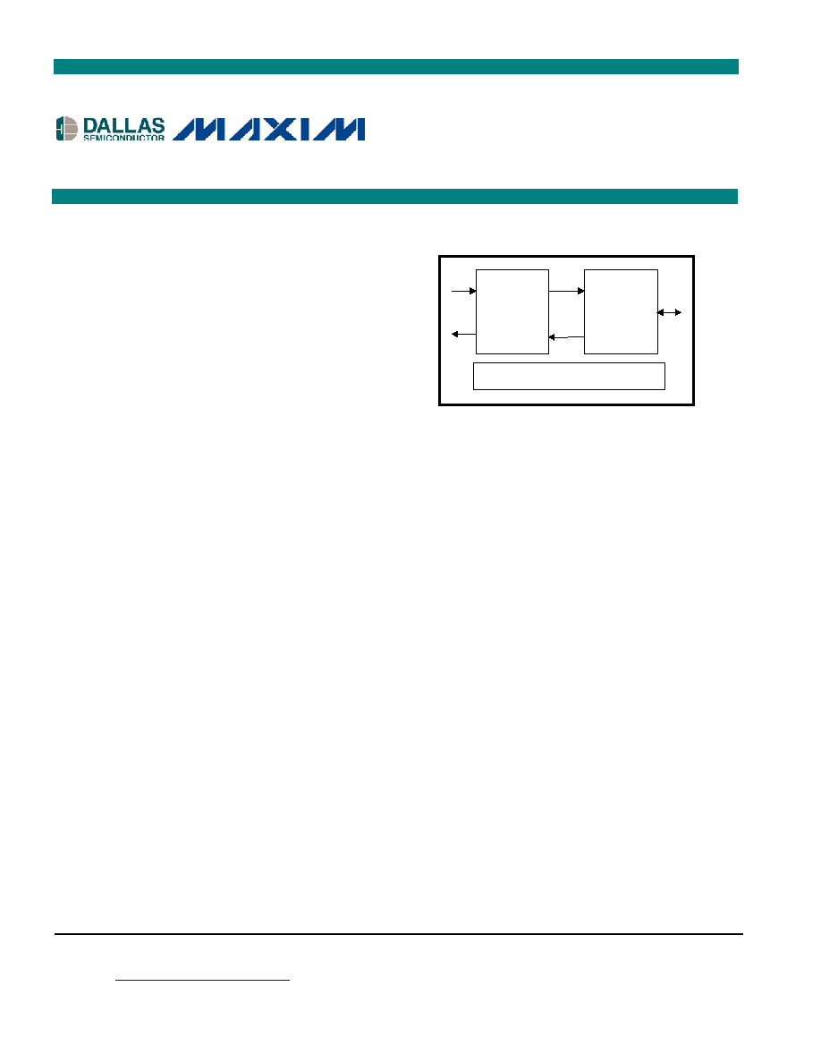
FUNCTIONAL DIAGRAM
APPLICATIONS
§ Routers
§ Switches
§ Test Equipment
§ Aggregators/Concentrators
§ PBX
§ Base Stations
DESCRIPTION
The DS3160 device, which combines a line interface unit (LIU) with a formatter and framer, is compliant
with the JT 6312kbps secondary-rate user-network interface and supports the G.704 and NTT J2 frame
formats. A full-featured LIU with integrated jitter attenuator supports a software-programmable framer
and formatter. Framer features include alarm and error detection, on-chip HDLC controller for processing
of M-bit information, and programmable timeslot data-enable signal for 1.5Mbps, 3Mbps, 4.5Mbps, and
6Mbps frame formats. The formatter adds the required overhead to the user data and has the additional
capability of generating diagnostic errors. Loopback features, together with an on-chip bit-error-rate test
(BERT) function, allow easy isolation and monitoring of network segments.
FRAMER
AND
FORMATTER
CONTROL AND STATUS PORT
LINE
INTERFACE
UNIT
www.maxim-ic.com
DS3160
JT 6312kbps Secondary-Rate
Line Interface Unit
and Framer/Formatter

DS3160
2 of 107
1. MAIN FEATURES
Line Interface Unit
§ Integrated transmit and receive 6312kbps line interface
§ Requires no special external components other than 1:1 transformers
§ Transmit and receive signal-monitor outputs
§ Transmit, receive, and monitor paths use the same transformer (1:1)
§ Nominal pulse waveform: 2V
o-p
±0.3V, 50% pulse width
§ Electrical characteristics in accordance with TTC Standard JT-G703
§ Adaptive receive equalizer adapts to coax cable loses from 0 to 15dB
§ Performs clock/data recovery and wave shaping
§ Transmit line-driver monitoring checks for faulty transmitter or a shorted output
§ Jitter attenuator that can be placed either in the receive path or the transmit path or disabled
§ On-board B8ZS coder/decoder with the option to be disabled
§ Analog and digital loopbacks
§ Analog loss of signal detector
§ Tri-state-capable transmit and signal monitor line drivers for power management options
§ Commercial temperature operating range: 0°C to +70°C
Framer/Formatter
§ Provides frame synchronization and insertion
§ Frame structure in accordance with TTC Standard JT-G704
§ Frame alignment and cyclic redundancy check (CRC) in accordance with TTC Standard JT-G706
§ Alarm detection and generation
§ AIS and RAI generation
§ Supports maintenance data link using an integrated HDLC controller
§ Supports generation of gapped receive and transmit clocks for interface to devices that only need
access to selected timeslots
§ Programmable fractional circuit rates:
TS1-24 (1.5Mbps)
TS1-48 (3Mbps)
TS1-72 (4.5Mbps)
TS1-96 (6Mbps)
Path-Maintenance Data-Link HDLC Controller
§ Designed to handle multiple LAPD messages without host intervention
§ 256-byte receive and transmit buffers
§ Handles all of the normal Layer 2 tasks such as zero stuffing/destuffing, CRC generation/checking,
abort generation/checking, flag generation/detection, and byte alignment
§ Programmable high and low watermarks for the FIFO

DS3160
3 of 107
BERT
§ Can generate and detect the pseudorandom patterns of 2
7
- 1, 2
11
- 1, 2
15
- 1, and quasirandom signal
source (QRSS) as well as repetitive patterns from 1 to 32 bits in length
§ Large error counter (24 bits) allows testing to proceed for long periods without host intervention
§ Errors can be inserted into the generated BERT patterns for diagnostic purposes
Diagnostics
§ Diagnostic loopbacks (transmit to receive)
§ Line loopbacks (receive to transmit)
§ Payload loopback
§ Error counters for bipolar violations, code violations, loss of frame (LOF), framing bit errors, and
CRC errors
§ Error counters can be either updated automatically on 1-second boundaries as timed by the DS3160,
or by software control, or by an external hardware pulse
§ Can insert the bipolar violation errors and framing bit errors
§ Inserted errors can be either controlled by software or by an external hardware pulse
§ Generates loss of frame
Control Port
§ Nonmultiplexed or multiplexed 16-bit control port (with an optional 8-bit mode)
§ Intel and Motorola bus compatible
Packaging and Power
§ 3.3V low-power CMOS with 5V tolerant inputs and outputs
§ 100-pin LQFP package
§ IEEE 1149.1 JTAG test port

DS3160
4 of 107
Table 1A. APPLICABLE STANDARDS
1) Telecommunications Technique Council (TTC) JT-G.703, 1989 "Physical/Electrical Characteristics
of Hierarchical Digital Interfaces"
2) Telecommunications Technique Council (TTC) JT-G.704, 1989 "Synchronous Frame Structures
Used at Primary and Secondary Hierarchical Levels"
3) Telecommunications Technique Council (TTC) JT-G.706, 1989 "Frame Synchronization and CRC
Procedure"
4) International Telecommunication Union (ITU) G.703, April 1991 "Physical/Electrical Characteristics
of Hierarchical Digital Interfaces"
5) International Telecommunication Union (ITU) G.704, July 1995 "Synchronous Frame Structures
Used at 1544kbps, 6312kbps, 2048kbps, 8488kbps, and 44736kbps Hierarchical Levels"
6) International Telecommunication Union (ITU) G.775, November 1994 "Loss-of-Signal (LOS) and
Alarm Indication Signal (AIS) Defect Detection and Clearance Criteria"
7) International Telecommunication Union (ITU) G.783, January 1994 "Characteristics of Synchronous
Digital Hierarchy (SDH) Equipment Functional Blocks"
8) International Telecommunication Union (ITU) O.151, October 1992 "Error Performance Measuring
Equipment Operating at the Primary Rate and Above"
9) International Telecommunication Union (ITU) O.153, October 1992 "Basic Parameters for the
Measurement of Error Performance at Bit Rates Below the Primary Rate"
10) International Telecommunication Union (ITU) O.161, 1984 "In-Service Code Violation Monitors for
Digital Systems"
DS3160
5 of 107
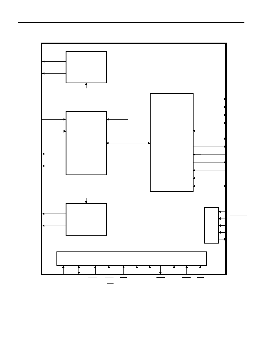
Figure 1A. BLOCK DIAGRAM
JT2 FRAMER/
FORMATTER
JT2 LIU
TRANSMIT
MONITOR
Rx+
Rx-
Tx+
Tx-
TxMON+
TxMON-
JTAG
TEST
BLOCK
JTMS
JTDO
JTDI
JTCLK
CPU INTERFACE AND GLOBAL CONFIGURATION
(ROUTED TO ALL BLOCKS)
CD0
CD15
CA0
CA7
CWR
(CR
W
)
CRD
(
CDS
)
CCS
CIM
CINT
CMS
TEST
RST
CALE
RECEIVE
MONITOR
RxMON+
RxMON-
FRSOF
FRCLK
FRD
FRDEN
FRLOF
FRLOS
FRMECU
FTCLK
FTD
FTDEN
FTSOF
FTMEI
MCLK
DS3160
JTRST