1 of 24
072303
FEATURES
Ï Lithium-Ion (Li+) Safety Circuit
- Overvoltage Protection
- Overcurrent/Short-Circuit Protection
- Undervoltage Protection
Ï Zero Volt Battery Recovery Charge
Ï Available in Two Configurations:
- Internal 25m
W Sense Resistor
- External User-Selectable Sense Resistor
Ï Current Measurement
- 12-Bit Bidirectional Measurement
- Internal Sense Resistor Configuration:
0.625mA LSB and Ý1.9A Dynamic Range
- External Sense Resistor Configuration:
15.625
mV LSB and Ý64mV Dynamic
Range
Ï Current Accumulation:
- Internal Sense Resistor: 0.25mAhr LSB
- External Sense Resistor: 6.25
mVhr LSB
Ï Voltage Measurement with 4.88mV
Resolution
Ï Temperature Measurement Using Integrated
Sensor with 0.125
¯C Resolution
Ï System Power Management and Control
Feature Support
Ï 32 Bytes of Lockable EEPROM
Ï 16 Bytes of General-Purpose SRAM
Ï Dallas 1-Wire
Û
Interface with Unique 64-bit
Device Address
Ï Low Power Consumption:
- Active Current: 60
mA typ, 90mA max
- Sleep Current:
1
mA typ, 2mA max
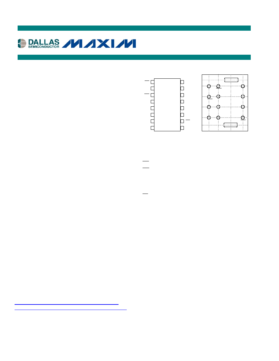
PIN CONFIGURATION
PIN DESCRIPTION
CC
- Charge Control Output
DC
- Discharge Control Output
DQ - Data Input/Output
PIO - Programmable I/O Pin
PLS - Battery Pack Positive Terminal Input
PS
- Power Switch Sense Input
V
IN
- Voltage-Sense Input
V
DD
- Power-Supply Input (2.5V to 5.5V)
V
SS
- Device Ground
SNS - Sense Resistor Connection
IS1 - Current-Sense Input
IS2 - Current-Sense Input
SNS Probe
- Do Not Connect
V
SS
Probe
- Do Not Connect
DS2761
High-Precision Li+ Battery Monitor
www.maxim-ic.com
CC
V
IN
V
DD
PIO
V
SS
V
SS
V
SS
PS
IS1
DS2761
16-Pin TSSOP Package
IS2
SNS
SNS
1
2
2
3
2
1
4
5
6
7
8
16
15
14
13
12
11
10
9
SNS
DQ
PLS
DC
1-Wire is a registered trademark of Dallas Semiconductor.
DS2761
Flip-Chip Packaging*
Top View
PLS DC DQ
CC IS2
VIN IS1
VDD PIO PS
SNS
VSS
1 2 3 4
A
B
C
D
E
F
SNS
Probe
VSS
Probe
* Mechanical drawing for the 16-pin TSSOP and DS2761 flip-chip package can be found at:
http://pdfserv.maxim-ic.com/arpdf/Packages/16tssop.pdf
http://pdfserv.maxim-ic.com/arpdf/Packages/chips/2761x.pdf

DS2761
2 of 24
ORDERING INFORMATION
PART
MARKING DESCRIPTION
DS2761AE
D2761EA
TSSOP, External Sense Resistor, 4.275V V
OV
DS2761BE
D2761EB
TSSOP, External Sense Resistor, 4.35V V
OV
DS2761AE/T&R
D2761EA
DS2761AE on Tape-and-Reel
DS2761BE/T&R
D2761EB
DS2761BE on Tape-and-Reel
DS2761AE-025
2761A25
TSSOP, 25m
W Sense Resistor, 4.275V V
OV
DS2761BE-025
2761B25
TSSOP, 25m
W Sense Resistor, 4.35V V
OV
DS2761AE-025/T&R 2761A25
DS2761AE-025 in Tape-and-Reel
DS2761BE-025/T&R 2761B25
DS2761BE-025 in Tape-and-Reel
DS2761AX-025/T&R DS2761AR Flip-Chip, 25m
W Sense Resistor, Tape-and-Reel, 4.275V V
OV
DS2761BX-025/T&R DS2761BR
Flip-Chip, 25m
W Sense Resistor, Tape-and-Reel, 4.35V V
OV
DS2761AX/T&R
DS2761A
Flip-Chip, External Sense Resistor, Tape-and-Reel, 4.275V V
OV
DS2761BX/T&R
DS2761B
Flip-Chip, External Sense Resistor, Tape-and-Reel, 4.35V V
OV
Note: Additional V
OV
options are available, contact Maxim/Dallas Semiconductor sales.
DESCRIPTION
The DS2761 high-precision Li+ battery monitor is a data-acquisition, information-storage, and safety-
protection device tailored for cost-sensitive battery pack applications. This low-power device integrates
precise temperature, voltage, and current measurement, nonvolatile (NV) data storage, and Li+ protection
into the small footprint of either a TSSOP package or flip-chip package. The DS2761 is a key component
in applications including remaining capacity estimation, safety monitoring, and battery-specific data
storage.
Through its 1-Wire interface, the DS2761 gives the host system read/write access to status and control
registers, instrumentation registers, and general-purpose data storage. Each device has a unique factory-
programmed 64-bit net address that allows it to be individually addressed by the host system, supporting
multibattery operation.
The DS2761 is capable of performing temperature, voltage, and current measurement to a resolution
sufficient to support process monitoring applications such as battery charge control, remaining capacity
estimation, and safety monitoring. Temperature is measured using an on-chip sensor, eliminating the need
for a separate thermistor. Bidirectional current measurement and accumulation are accomplished using
either an internal 25m
W sense resistor or an external device. The DS2761 also features a programmable
I/O pin that allows the host system to sense and control other electronics in the pack, including switches,
vibration motors, speakers, and LEDs.
Three types of memory are provided on the DS2761 for battery information storage: EEPROM, lockable
EEPROM, and SRAM. EEPROM memory saves important battery data in true NV memory that is
unaffected by severe battery depletion, accidental shorts, or ESD events. Lockable EEPROM becomes
ROM when locked to provide additional security for unchanging battery data. SRAM provides
inexpensive storage for temporary data.

DS2761
3 of 24
Figure 1. BLOCK DIAGRAM
1-WIRE
INTERFACE
AND
ADDRESS
THERMAL
SENSE
MUX
VOLTAGE
REFERENCE
ADC
REGISTERS AND
USER MEMORY
25m
W
DQ
CHIP GROUND
+
-
LOCKABLE EEPROM
SRAM
TEMPERATURE
VOLTAGE
CURRENT
ACCUM. CURRENT
STATUS / CONTROL
LI-ION PROTECTION
V
IN
IS1
IS2
SNS
IS2
IS1
V
SS
CC
DC
PLS
PS
PIO
TIMEBASE
INTERNAL SENSE RESISTOR CONFIGURATION ONLY
I
TST
I
TST
I
RC
V
DD
V
SS
PLS
TEST CURRENT AND RECOVERY CHARGE DETAIL

DS2761
4 of 24
Table 1. DETAILED PIN DESCRIPTION
SYMBOL
TSSOP
FLIP
CHIP
DESCRIPTION
CC
1
C1
Charge Protection Control Output. Controls an external p-channel
high-side charge protection FET.
DC
3
B2
Discharge Protection Control Output. Controls an external p-channel
high-side discharge protection FET.
DQ
7
B4
Data Input/Out. 1-Wire data line. Open-drain output driver. Connect
this pin to the DATA terminal of the battery pack. Pin has an internal
1
mA pull-down for sensing disconnection.
PIO
14
E2
Programmable I/O Pin. Used to control and monitor user-defined
external circuitry. Open drain to VSS.
PLS
2
B1
Battery Pack Positive Terminal Input. The DS2761 monitors the pack
plus terminal through PLS to detect overcurrent and overload conditions,
as well as the presence of a charge source. Additionally, a charge path to
recover a deeply depleted cell is provided from PLS to V
DD
. In sleep
mode (with SWEN = 0), any capacitance or voltage source connected to
PLS is discharged internally to V
SS
through 200
mA (nominal) to assure
reliable detection of a valid charge source. For details of other internal
connections to PLS and associated conditions see the Li+ Protection
Circuitry section.
PS
10
E4
Power Switch Sense Input. The device wakes up from Sleep Mode
when it senses the closure of a switch to VSS on this pin. Pin has an
internal 1
mA pull-up to V
DD
.
VIN
16
D1
Voltage Sense Input. The voltage of the Li+ cell is monitored via this
input pin. This pin has a weak pullup to V
DD
.
V
DD
15
E1
Power Supply Input. Connect to the positive terminal of the Li+ cell
through a decoupling network.
VSS
13,14,
15
F3
Device Ground. Connect directly to the negative terminal of the Li+ cell.
For the external sense resistor configuration, connect the sense resistor
between VSS and SNS.
SNS
4,5,6
A3
Sense Resistor Connection. Connect to the negative terminal of the
battery pack. In the internal sense resistor configuration, the sense resistor
is connected between VSS and SNS.
IS1
9
D4
Current Sense Input. This pin is internally connected to VSS through a
4.7k
W resistor. Connect a 0.1mF capacitor between IS1 and IS2 to
complete a low-pass input filter.
IS2
8
C4
Current Sense Input. This pin is internally connected to SNS through a
4.7k
W resistor.
SNS
Probe
N/A
C2
Do Not Connect.
VSS
Probe
N/A
D2
Do Not Connect.
DS2761
5 of 24
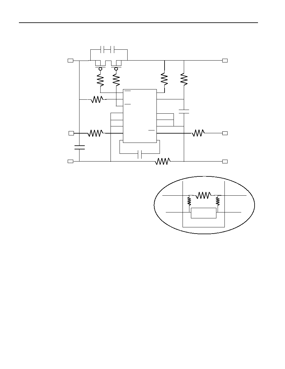
Figure 2. APPLICATION EXAMPLE
1) R
SNS
is present for external sense resistor configurations only.
2) R
SNS-INT
is present for internal sense resistor configurations only.
CC
PLS
DC
SNS
SNS
SNS
DQ
IS2
V
IN
V
DD
PIO
V
SS
V
SS
V
SS
PS
IS1
DS2761
104
102 x 2
104
SNS
DS2761
V
SS
IS2
IS1
4.
7K
W
4.
7K
W
voltage
sense
PACK+
PACK-
DATA
150
W
150
W
1k
W
150
W
1k
W
1k
W
102
BAT+
BAT-
R
SNS
(1)
R
SNS-INT
(2)
R
KS
R
KS
PS
4.7k
W
DS2761
6 of 24
POWER MODES
The DS2761 has two power modes: active and sleep. While in active mode, the DS2761 continually
measures current, voltage, and temperature to provide data to the host system and to support current
accumulation and Li+ safety monitoring. In sleep mode, the DS2761 ceases these activities. The DS2761
enters sleep mode when any of the following conditions occurs:
Ï The PMOD bit in the Status Register has been set to 1 and the DQ line is low for longer than
2s (pack disconnection)
Ï The voltage on V
IN
drops below undervoltage threshold V
UV
for t
UVD
(cell depletion)
Ï The pack is disabled through the issuance of a SWAP command (SWEN bit = 1)
The DS2761 returns to active mode when any of the following occurs:
Ï The PMOD bit has been set to 1 and the SWEN bit is set to 0 and the DQ line is pulled high
(pack connection)
Ï The
PS
pin is pulled low (power switch)
Ï The voltage on PLS becomes greater than the voltage on V
IN
(charger connection) with the SWEN bit
set to 0
Ï The pack is enabled through the issuance of a SWAP command (SWEN bit = 1)
The DS2761 defaults to sleep mode when power is first applied.
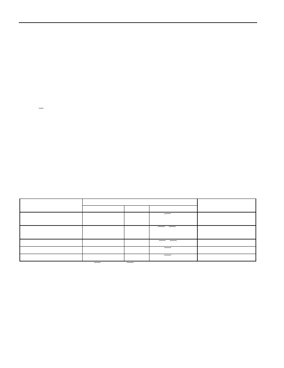
Li+ PROTECTION CIRCUITRY
During active mode, the DS2761 constantly monitors cell voltage and current to protect the battery from
overcharge (overvoltage), overdischarge (undervoltage), and excessive charge and discharge currents
(overcurrent, short circuit). Conditions and DS2761 responses are described in the sections below and
summarized in Table 2 and Figure 3.
Table 2. Li+ PROTECTION CONDITIONS AND DS2761 RESPONSES
ACTIVATION
CONDITION
NAME
THRESHOLD DELAY
RESPONSE
RELEASE
THRESHOLD
Overvoltage
V
IN
> V
OV
t
OVD
CC
high
V
IN
< V
CE
, or
V
IS
-2mV
Undervoltage
V
IN
< V
UV
t
UVD
CC
,
DC
high,
Sleep Mode
V
PLS
> V
DD
(1)
(charger connected)
Overcurrent, Charge
V
IS
> V
OC
(2)
t
OCD
CC
,
DC
high
V
PLS
< V
DD
- V
TP
(3)
Overcurrent, Discharge
V
IS
< -V
OC
(2)
t
OCD
DC
high
V
PLS
> V
DD
- V
TP
(4)
Short Circuit
V
SNS
> V
SC
t
SCD
DC
high
V
PLS
> V
DD
- V
TP
(4)
V
IS
= V
IS1
- V
IS2
. Logic high = V
PLS
for
CC
and V
DD
for
DC
.
All voltages are with respect to V
SS
. I
SNS
references current
delivered from pin SNS.
1)
If V
DD
< 2.2V, release is delayed until the recovery charge current (I
RC
) passed from PLS to V
DD
charges the battery and
allows V
DD
to exceed 2.2V.
2)
For the internal sense resistor configuration, the overcurrent thresholds are expressed in terms of current: I
SNS
> I
OC
for
charge direction and I
SNS
< -I
OC
for discharge direction
3)
With test current I
TST
flowing from PLS to V
SS
(pulldown on PLS)
4)
With test current I
TST
flowing from V
DD
to PLS (pullup on PLS)
Overvoltage. If the cell voltage on V
IN
exceeds the overvoltage threshold, V
OV
, for a period longer than
overvoltage delay, t
OVD
, the DS2761 shuts off the external charge FET and sets the OV flag in the
protection register. When the cell voltage falls below charge enable threshold V
CE
, the DS2761 turns the
DS2761
7 of 24
charge FET back on (unless another protection condition prevents it). Discharging remains enabled
during overvoltage, and the DS2761 re-enables the charge FET before V
IN
< V
CE
if a discharge current of
-80mA (V
IS
-2mV) or less is detected.
Undervoltage. If the voltage of the cell drops below undervoltage threshold V
UV
for a period longer than
undervoltage delay t
UVD
, the DS2761 shuts off the charge and discharge FETs, sets the UV flag in the
protection register, and enters sleep mode. The DS2761 provides a current-limited recovery charge path
from PLS to V
DD
to gently charge severely depleted cells during sleep mode.
Overcurrent, Charge Direction. The voltage difference between the IS1 pin and the IS2 pin (V
IS
= V
IS1
-
V
IS2
) is the filtered voltage drop across the current-sense resistor. If V
IS
exceeds overcurrent threshold
V
OC
for a period longer than overcurrent delay t
OCD
, the DS2761 shuts off both external FETs and sets the
COC flag in the protection register. The charge current path is not re-established until the voltage on the
PLS pin drops below V
DD
- V
TP
. The DS2761 provides a test current of value I
TST
from PLS to V
SS
to pull
PLS down in order to detect the removal of the offending charge current source.
Overcurrent, Discharge Direction. If V
IS
is less than -V
OC
for a period longer than t
OCD
, the DS2761
shuts off the external discharge FET and sets the DOC flag in the protection register. The discharge
current path is not re-established until the voltage on PLS rises above V
DD
- V
TP
. The DS2761 provides a
test current of value I
TST
from V
DD
to PLS to pull PLS up in order to detect the removal of the offending
low-impedance load.
Short Circuit. If the voltage on the SNS pin with respect to V
SS
exceeds short-circuit threshold V
SC
for a
period longer than short-circuit delay t
SCD
, the DS2761 shuts off the external discharge FET and sets the
DOC flag in the protection register. The discharge current path is not re-established until the voltage on
PLS rises above V
DD
- V
TP
. The DS2761 provides a test current of value I
TST
from V
DD
to PLS to pull
PLS up in order to detect the removal of the short circuit.
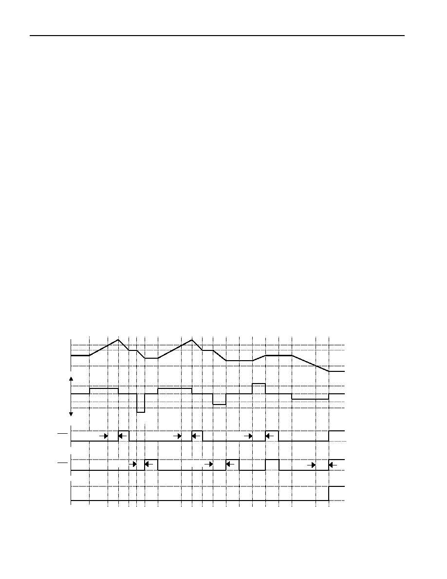
Figure 3. Li+ PROTECTION CIRCUITRY EXAMPLE WAVEFORMS
(1) To allow the device to react quickly to short circuits, detection occurs on the SNS pin rather than on the
filtered IS1 and IS2 pins. The actual short-circuit detect condition is V
SNS
> V
SC
.
SLEEP
MODE
V
OV
V
CE
V
UV
V
CELL
V
IS
CHARGE
DISCHARGE
CC
DC
-V
SC
V
OC
-V
OC
0
t
SCD
t
OCD
t
OCD
t
UVD
t
OVD
V
PLS
V
DD
ACTIVE
V
SS
V
SS
INACTIVE
t
OVD
(1)

DS2761
8 of 24
Summary. All of the protection conditions described above are OR'ed together to affect the
CC
and
DC
outputs.
DC
= (Undervoltage) or (Overcurrent, Either Direction) or (Short Circuit) or
(Protection Register Bit DE = 0) or (Sleep Mode)
CC
= (Overvoltage) or (Undervoltage) or (Overcurrent, Charge Direction) or (Protection Register
bit CE = 0) or (Sleep Mode)
CURRENT MEASUREMENT
In the active mode of operation, the DS2761 continually measures the current flow into and out of the
battery by measuring the voltage drop across a current-sense resistor. The DS2761 is available in two
configurations: 1) internal 25m
W current-sense resistor, and 2) external user-selectable sense resistor. In
either configuration, the DS2761 considers the voltage difference between pins IS1 and IS2 (V
IS
= V
IS1
-
V
IS2
) to be the filtered voltage drop across the sense resistor. A positive V
IS
value indicates current is
flowing into the battery (charging), while a negative V
IS
value indicates current is flowing out of the
battery (discharging).
V
IS
is measured with a signed resolution of 12-bits. The current register is updated in two's-complement
format every 88ms (128/fsample) with an average of 128 readings. Currents outside the range of the
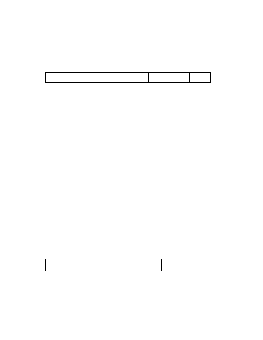
register are reported at the limit of the range. The format of the current register is shown in Figure 4.
For the internal sense resistor configuration, the DS2761 maintains the current register in units of amps,
with a resolution of 0.625mA and full-scale range of no less than
Ý1.9A (see Note 7 on I
FS
spec for more
details). The DS2761 automatically compensates for internal sense resistor process variations and
temperature effects when reporting current.
For the external sense resistor configuration, the DS2761 writes the measured V
IS
voltage to the current
register, with a resolution of 15.625
mV and a full-scale range of Ý64mV.
Figure 4. CURRENT REGISTER FORMAT
MSB--Address 0E
LSB--Address 0F
S
2
11
2
10
2
9
2
8
2
7
2
6
2
5
2
4
2
3
2
2
2
1
2
0
X
X
X
MSb
LSb
MSb
LSb
Units: 0.625mA for Internal Sense Resistor
15.625
mV for External Sense Resistor
CURRENT ACCUMULATOR
The current accumulator facilitates remaining capacity estimation by tracking the net current flow into
and out of the battery. Current flow into the battery increments the current accumulator while current
flow out of the battery decrements it. Data is maintained in the current accumulator in two's-complement
format. The format of the current accumulator is shown in Figure 5.
DS2761
9 of 24
When the internal sense resistor is used, the DS2761 maintains the current accumulator in units of amp-
hours, with a resolution of 0.25mAhrs and full-scale range of
Ý8.2Ahrs. When using an external sense
resistor, the DS2761 maintains the current accumulator in units of volt-hours, with a resolution of
6.25
mVhrs and a full scale range of Ý205mVhrs.
The current accumulator is a read/write register that can be altered by the host system as needed.
Figure 5. CURRENT ACCUMULATOR FORMAT
MSB--Address 10
LSB--Address 11
S
2
14
2
13
2
12
2
11
2
10
2
9
2
8
2
7
2
6
2
5
2
4
2
3
2
2
2
1
2
0
MSb
LSb
MSb
LSb
Units: 0.25mAhrs for Internal Sense Resistor
6.25
mVhrs for External Sense Resistor
CURRENT OFFSET COMPENSATION
Current measurement and current accumulation are both internally compensated for offset on a continual
basis minimizing error resulting from variations in device temperature and voltage. Additionally, a
constant bias can be utilized to alter any other sources of offset. This bias resides in EEPROM address
33h in two's-complement format and is subtracted from each current measurement. The current offset
bias is applied to both the internal and external sense resistor configurations. The factory default for the
current offset bias is a value of 0.
Figure 6. CURRENT OFFSET BIAS
Address 33
S
2
6
2
5
2
4
2
3
2
2
2
1
2
0
MSb
LSb
Units: 0.625mA for Internal Sense Resistor
15.625
mV for External Sense Resistor
VOLTAGE MEASUREMENT
The DS2761 continually measures the voltage between pins V
IN
and V
SS
over a range of 0 to 4.75V. The
voltage register is updated in two's-complement format every 3.4ms with a resolution of 4.88mV.
Voltages above the maximum register value are reported as the maximum value. The voltage register
format is shown in Figure 7.
DS2761
10 of 24
Figure 7. VOLTAGE REGISTER FORMAT
MSB--Address 0C
LSB--Address 0D
S
2
9
2
8
2
7
2
6
2
5
2
4
2
3
2
2
2
1
2
0
X
X
X
X
X
MSb
LSb
MSb
LSb
Units: 4.88mV
TEMPERATURE MEASUREMENT
The DS2761 uses an integrated temperature sensor to continually measure battery temperature.
Temperature measurements are placed in the temperature register every 220ms in two's-complement
format with a resolution of 0.125¯C over a range of
Ý127¯C. The temperature register format is shown in
Figure 8.
Figure 8. TEMPERATURE REGISTER FORMAT
MSB--Address 18
LSB--Address 19
S
2
9
2
8
2
7
2
6
2
5
2
4
2
3
2
2
2
1
2
0
X
X
X
X
X
MSb
LSb
MSb
LSb
Units: 0.125
¯C
PROGRAMMABLE I/O
To use the PIO pin as an output, write the desired output value to the PIO bit in the special feature
register. Writing a 0 to the PIO bit enables the PIO output driver, pulling the PIO pin to V
SS
. Writing a 1
to the PIO bit disables the output driver, allowing the PIO pin to be pulled high or used as an input. To
sense the value on the PIO pin, read the PIO bit. The DS2761 turns off the PIO output driver and sets the
PIO bit high when in sleep mode or when DQ is low for more than 2s, regardless of the state of the
PMOD bit.
POWER SWITCH INPUT
The DS2761 provides a power control function that uses the discharge protection FET to gate battery
power to the system. The
PS
pin, internally pulled to V
DD
through a 1
mA current source, is continuously
monitored for a low-impedance connection to V
SS
. If the DS2761 is in sleep mode, the detection of a low
on the
PS
pin causes the device to transition into active mode, turning on the discharge FET. If the
DS2761 is already in active mode, activity on
PS
has no effect other than the latching of its logic low
level in the
PS
bit in the special feature register. The reading of a 0 in the
PS
bit should be immediately
followed by writing a 1 to the
PS
bit to ensure that a subsequent low forced on the
PS
pin is latched into
the
PS
bit.
DS2761
11 of 24
MEMORY
The DS2761 has a 256-byte linear address space with registers for instrumentation, status, and control in
the lower 32 bytes, with lockable EEPROM and SRAM memory occupying portions of the remaining
address space. All EEPROM and SRAM memory is general purpose except addresses 30h, 31h, and 33h,
which should be written with the default values for the protection register, status register, and current
offset register, respectively. When the MSB of any two-byte register is read, both the MSB and LSB are
latched and held for the duration of the read data command to prevent updates during the read and ensure
synchronization between the two register bytes. For consistent results, always read the MSB and the LSB
of a two-byte register during the same read data command sequence.
EEPROM memory is shadowed by RAM to eliminate programming delays between writes and to allow
the data to be verified by the host system before being copied to EEPROM. All reads and writes to/from
EEPROM memory actually access the shadow RAM. In unlocked EEPROM blocks, the write data
command updates shadow RAM. In locked EEPROM blocks, the write data command is ignored. The
copy data command copies the contents of shadow RAM to EEPROM in an unlocked block of EEPROM
but has no effect on locked blocks. The recall data command copies the contents of a block of EEPROM
to shadow RAM regardless of whether the block is locked or not.
Table 3. MEMORY MAP
ADDRESS (HEX)
DESCRIPTION
READ/WRITE
00
Protection Register
R/W
01
Status Register
R
02Ù06
Reserved
07
EEPROM Register
R/W
08
Special Feature Register
R/W
09Ù0B
Reserved
0C
Voltage Register MSB
R
0D
Voltage Register LSB
R
0E
Current Register MSB
R
0F
Current Register LSB
R
10
Accumulated Current Register MSB
R/W
11
Accumulated Current Register LSB
R/W
12Ù17
Reserved
18
Temperature Register MSB
R
19
Temperature Register LSB
R
1AÙ1F
Reserved
20Ù2F
EEPROM, block 0
R/W*
30Ù3F
EEPROM, block 1
R/W*
40Ù7F
Reserved
80Ù8F
SRAM
R/W
90ÙFF
Reserved
* Each EEPROM block is read/write until locked by the LOCK command, after which it is read-only.
DS2761
12 of 24
PROTECTION REGISTER
The protection register consists of flags that indicate protection circuit status and switches that give
conditional control over the charging and discharging paths. Bits OV, UV, COC, and DOC are set when
corresponding protection conditions occur and remain set until cleared by the host system. The default
values of the CE and DE bits of the protection register are stored in lockable EEPROM in the
corresponding bits in address 30h. A recall data command for EEPROM block 1 recalls the default values
into CE and DE. The format of the protection register is shown in Figure 9. The function of each bit is
described in detail in the following paragraphs.
Figure 9. PROTECTION REGISTER FORMAT
Address 00
Bit 7
Bit 6
Bit 5
Bit 4
Bit 3
Bit 2
Bit 1
Bit 0
OV
UV
COC
DOC
CC
DC
CE
DE
OV--Overvoltage Flag. When set to 1, this bit indicates the battery pack has experienced an overvoltage
condition. This bit must be reset by the host system.
UV--Undervoltage Flag. When set to 1, this bit indicates the battery pack has experienced an
undervoltage condition. This bit must be reset by the host system.
COC--Charge Overcurrent Flag. When set to 1, this bit indicates the battery pack has experienced a
charge-direction overcurrent condition. This bit must be reset by the host system.
DOC--Discharge Overcurrent Flag. When set to 1, this bit indicates the battery pack has experienced a
discharge-direction overcurrent condition. This bit must be reset by the host system.
CC -- CC Pin Mirror. This read-only bit mirrors the state of the CC output pin.
DC -- DC Pin Mirror. This read-only bit mirrors the state of the DC output pin.
CE--Charge Enable. Writing a 0 to this bit disables charging ( CC output high, external charge FET off)
regardless of cell or pack conditions. Writing a 1 to this bit enables charging, subject to override by the
presence of any protection conditions. The DS2761 automatically sets this bit to 1 when it transitions
from sleep mode to active mode.
DE--Discharge Enable. Writing a 0 to this bit disables discharging ( DC output high, external discharge
FET off) regardless of cell or pack conditions. Writing a 1 to this bit enables discharging, subject to
override by the presence of any protection conditions. The DS2761 automatically sets this bit to 1 when it
transitions from sleep mode to active mode.
STATUS REGISTER
The default values for the status register bits are stored in lockable EEPROM in the corresponding bits of
address 31h. A recall data command for EEPROM block 1 recalls the default values into the status
register bits. The format of the status register is shown in Figure 10. The function of each bit is described
in detail in the following paragraphs.

DS2761
13 of 24
Figure 10. STATUS REGISTER FORMAT
Address 01
Bit 7
Bit 6
Bit 5
Bit 4
Bit 3
Bit 2
Bit 1
Bit 0
X
X
PMOD
RNAOP
SWEN
X
X
X
PMOD--Sleep Mode Enable. A value of 1 in this bit enables the DS2761 to enter sleep mode when the
DQ line goes low for greater than 2s and to leave sleep mode when the DQ line goes high. A value of 0
disables DQ-related transitions into and out of sleep mode. This bit is read-only. The desired default value
should be set in bit 5 of address 31h. The factory default is 0.
RNAOP--Read Net Address Opcode. A value of 0 in this bit sets the opcode for the read net address
command to 33h, while a 1 sets the opcode to 39h. This bit is read-only. The desired default value should
be set in bit 4 of address 31h. The factory default is 0.
SWEN--SWAP Command Enable. A value of 1 in this bit location enables the recognition of a SWAP
command. If set to 0, SWAP commands are ignored. The desired default value should be set in bit 3 of
address 31h. This bit is read-only. The factory default is 0.
X--Reserved Bits.
EEPROM REGISTER
The format of the EEPROM register is shown in Figure 11. The function of each bit is described in detail
in the following paragraphs.
Figure 11. EEPROM REGISTER FORMAT
Address 07
Bit 7
Bit 6
Bit 5
Bit 4
Bit 3
Bit 2
Bit 1
Bit 0
EEC
LOCK
X
X
X
X
BL1
BL0
EEC--EEPROM Copy Flag. A 1 in this read-only bit indicates that a copy data command is in progress.
While this bit is high, writes to EEPROM addresses are ignored. A 0 in this bit indicates that data may be
written to unlocked EEPROM blocks.
LOCK--EEPROM Lock Enable. When this bit is 0, the lock command is ignored. Writing a 1 to this bit
enables the lock command. After the lock command is executed, the LOCK bit is reset to 0. The factory
default is 0.
BL1--EEPROM Block 1 Lock Flag. A 1 in this read-only bit indicates that EEPROM block 1 (addresses
30 to 3F) is locked (read-only) while a 0 indicates block 1 is unlocked (read/write).
BL0--EEPROM Block 0 Lock Flag. A 1 in this read-only bit indicates that EEPROM block 0 (addresses
20 to 2F) is locked (read-only) while a 0 indicates block 0 is unlocked (read/write).
X--Reserved Bits.
DS2761
14 of 24
SPECIAL FEATURE REGISTER
The format of the special feature register is shown in Figure 12. The function of each bit is described in
detail in the following paragraphs.
Figure 12. SPECIAL FEATURE REGISTER FORMAT
Address 08
Bit 7
Bit 6
Bit 5
Bit 4
Bit 3
Bit 2
Bit 1
Bit 0
PS
PIO
MSTR
X
X
X
X
X
PS -- PS Pin Latch. This bit latches a low state on the PS pin, and is cleared only by writing a 1 to this
location. Writing this bit to a 1 immediately upon reading of a 0 value is recommended.
PIO--PIO Pin Sense and Control. See the Programmable I/O section for details on this read/write bit.
MSTR--SWAP Master Status Bit. This bit indicates whether a device has been selected through the
SWAP command. Selection of this device through the SWAP command and the appropriate net address
results in setting this bit, indicating that this device is the master. A 0 signifies that this device is not the
master.
X--Reserved Bits.
1-WIRE BUS SYSTEM
The 1-Wire bus is a system that has a single bus master and one or more slaves. A multidrop bus is a 1-
Wire bus with multiple slaves. A single-drop bus has only one slave device. In all instances, the DS2761
is a slave device. The bus master is typically a microprocessor in the host system. The discussion of this
bus system consists of four topics: 64-bit net address, hardware configuration, transaction sequence, and
1-Wire signaling.
64-BIT NET ADDRESS
Each DS2761 has a unique, factory-programmed 1-Wire net address that is 64 bits in length. The first
eight bits are the 1-Wire family code (30h for DS2761). The next 48 bits are a unique serial number. The
last eight bits are a cyclic redundancy check (CRC) of the first 56 bits (see Figure 13). The 64-bit net
address and the 1-Wire I/O circuitry built into the device enable the DS2761 to communicate through the
1-Wire protocol detailed in the 1-Wire Bus System section of this data sheet.
Figure 13. 1-WIRE NET ADDRESS FORMAT
8-BIT CRC
48-BIT SERIAL NUMBER
8-BIT FAMILY
CODE (30H)
MSb
LSb
CRC GENERATION
The DS2761 has an 8-bit CRC stored in the most significant byte of its 1-Wire net address. To ensure
error-free transmission of the address, the host system can compute a CRC value from the first 56 bits of
the address and compare it to the CRC from the DS2761. The host system is responsible for verifying the
CRC value and taking action as a result. The DS2761 does not compare CRC values and does not prevent
DS2761
15 of 24
a command sequence from proceeding as a result of a CRC mismatch. Proper use of the CRC can result
in a communication channel with a very high level of integrity.
The CRC can be generated by the host using a circuit consisting of a shift register and XOR gates as
shown in Figure 10, or it can be generated in software. Additional information about the Dallas 1-Wire
CRC is available in Application Note 27, Understanding and Using Cyclic Redundancy Checks with
Dallas Semiconductor Touch Memory Products
. (This application not can be found on the Maxim/Dallas
Semiconductor website at www.maxim-ic.com).
In the circuit in Figure 14, the shift register bits are initialized to 0. Then, starting with the least
significant bit of the family code, one bit at a time is shifted in. After the 8th bit of the family code has
been entered, then the serial number is entered. After the 48th bit of the serial number has been entered,
the shift register contains the CRC value.
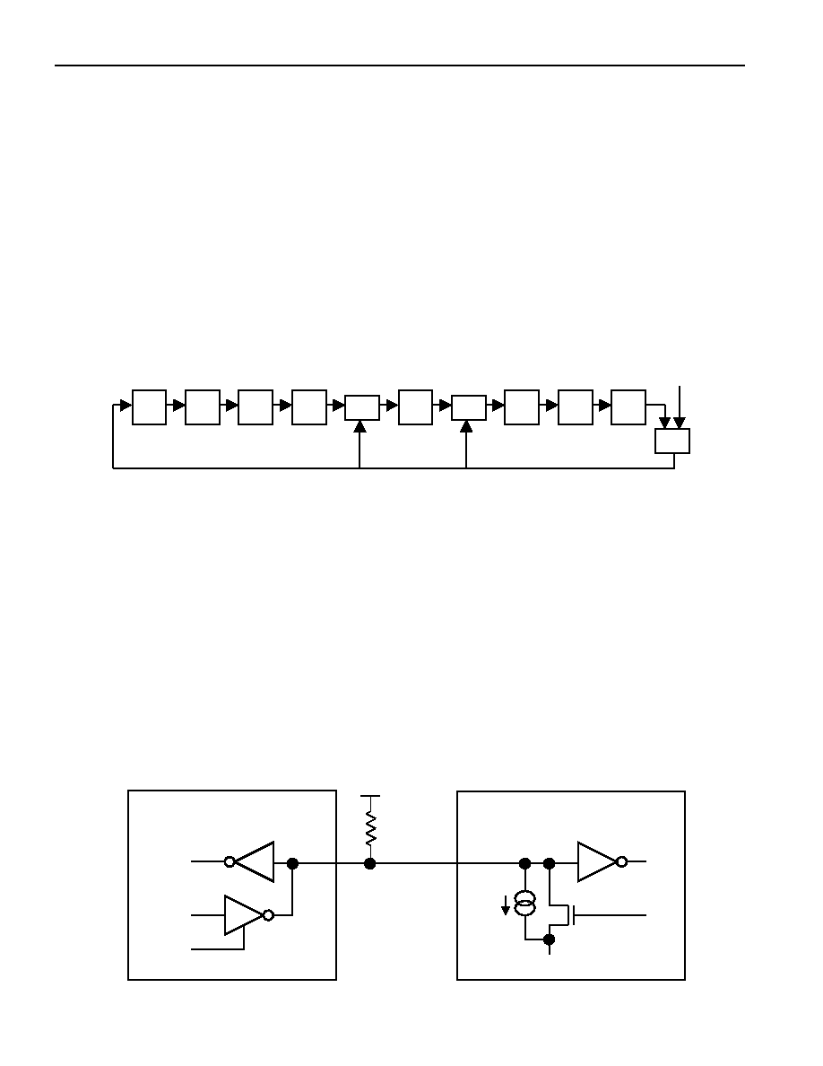
Figure 14. 1-WIRE CRC GENERATION BLOCK DIAGRAM
HARDWARE CONFIGURATION
Because the 1-Wire bus has only a single line, it is important that each device on the bus be able to drive
it at the appropriate time. To facilitate this, each device attached to the 1-Wire bus must connect to the
bus with open-drain or tri-state output drivers. The DS2761 used an open-drain output driver as part of
the bidirectional interface circuitry shown in Figure 15. If a bidirectional pin is not available on the bus
master, separate output and input pins can be connected together.
The 1-Wire bus must have a pullup resistor at the bus-master end of the bus. For short line lengths, the
value of this resistor should be approximately 5k
W. The idle state for the 1-Wire bus is high. If, for any
reason, a bus transaction must be suspended, the bus must be left in the idle state in order to properly
resume the transaction later. If the bus is left low for more than 120
m
s, slave devices on the bus begin to
interpret the low period as a reset pulse, effectively terminating the transaction.
Figure 15. 1-WIRE BUS INTERFACE CIRCUITRY
1
m
A
(typ)
100
W
MOSFET
Tx
Rx
Rx
Tx
Rx = RECEIVE
Tx = TRANSMIT
Vpullup
(2.0V to 5.5V)
4.7k
W
BUS MASTER
DS2761 1-WIRE PORT
MSb
XOR
XOR
LSb
XOR
INPUT

DS2761
16 of 24
TRANSACTION SEQUENCE
The protocol for accessing the DS2761 through the 1-Wire port is as follows:
Ï Initialization
Ï Net Address Command
Ï Function Command
Ï Transaction/Data
The sections that follow describe each of these steps in detail.
All transactions of the 1-Wire bus begin with an initialization sequence consisting of a reset pulse
transmitted by the bus master followed by a presence pulse simultaneously transmitted by the DS2761
and any other slaves on the bus. The presence pulse tells the bus master that one or more devices are on
the bus and ready to operate. For more details, see the 1-Wire Signaling section.
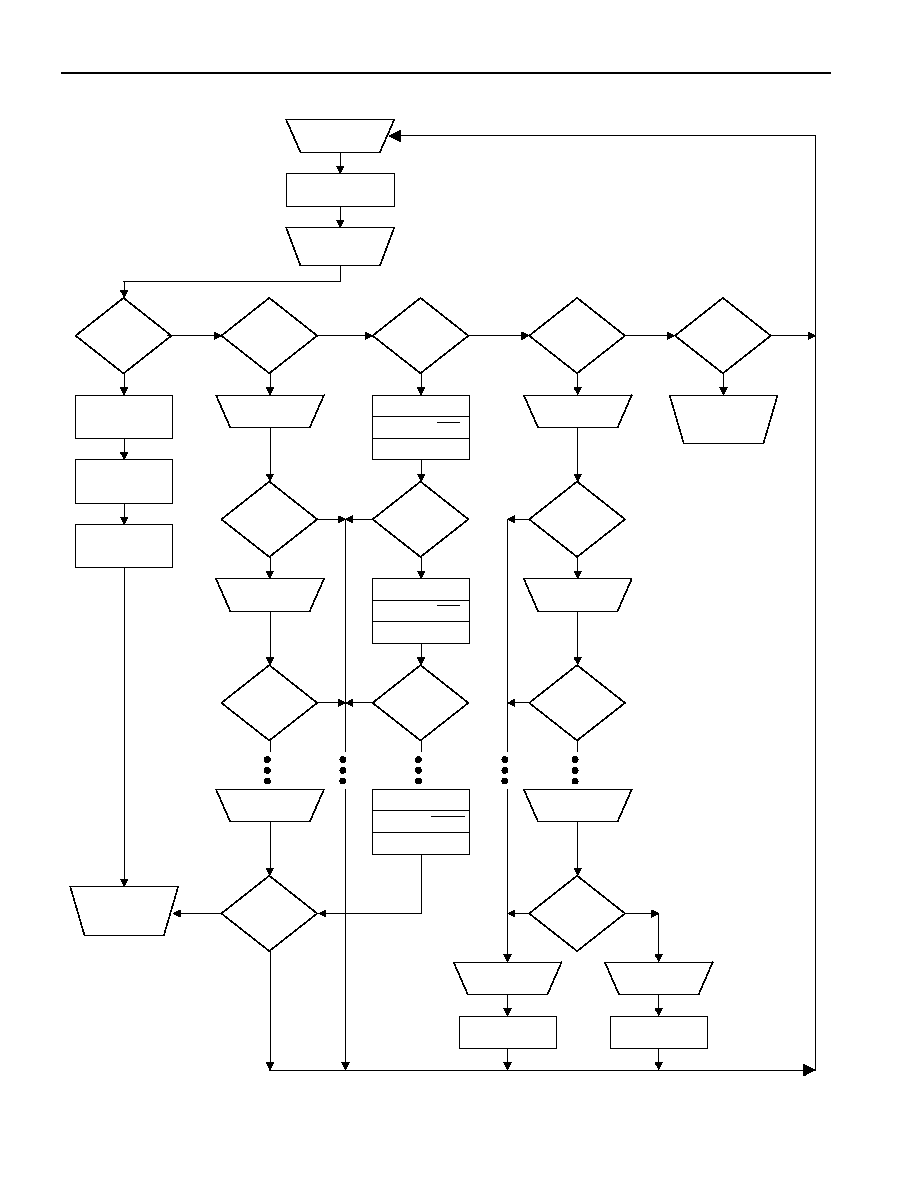
NET ADDRESS COMMANDS
Once the bus master has detected the presence of one or more slaves, it can issue one of the net address
commands described in the following paragraphs. The name of each ROM command is followed by the
8-bit opcode for that command in square brackets. Figure 16 presents a transaction flowchart of the net
address commands.
Read Net Address [33h or 39h]. This command allows the bus master to read the DS2761's 1-Wire net
address. This command can only be used if there is a single slave on the bus. If more than one slave is
present, a data collision occurs when all slaves try to transmit at the same time (open drain produces a
wired-AND result). The RNAOP bit in the status register selects the opcode for this command, with
RNAOP = 0 indicating 33h, and RNAOP = 1 indicating 39h.
Match Net Address [55h]. This command allows the bus master to specifically address one DS2761 on
the 1-Wire bus. Only the addressed DS2761 responds to any subsequent function command. All other
slave devices ignore the function command and wait for a reset pulse. This command can be used with
one or more slave devices on the bus.
Skip Net Address [CCh]. This command saves time when there is only one DS2761 on the bus by
allowing the bus master to issue a function command without specifying the address of the slave. If more
than one slave device is present on the bus, a subsequent function command can cause a data collision
when all slaves transmit data at the same time.
Search Net Address [F0h]. This command allows the bus master to use a process of elimination to
identify the 1-Wire net addresses of all slave devices on the bus. The search process involves the
repetition of a simple three-step routine: read a bit, read the complement of the bit, then write the desired
value of that bit. The bus master performs this simple three-step routine on each bit location of the net
address. After one complete pass through all 64 bits, the bus master knows the address of one device. The
remaining devices can then be identified on additional iterations of the process. See Chapter 5 of the Book
of DS19xx iButton
Û
Standards
for a comprehensive discussion of a net address search, including an actual
example. (This publication can be found on the Maxim/Dallas Semiconductor website at www.maxim-
ic.com).

DS2761
17 of 24
SWAP [AAh]. SWAP is a ROM level command specifically intended to aid in distributed multiplexing
applications and is described specifically with regards to power control using the 27xx series of products.
The term power control refers to the ability of the DS2761 to control the flow of power into or out the
battery pack using control pins DC
and CC . The SWAP command is issued followed by the net address.
The effect is to cause the addressed device to enable power to or from the system while simultaneously
(break-before-make) deselecting and powering down (SLEEP) all other packs. This switching sequence is
controlled by a timing pulse issued on the DQ line following the net address. The falling edge of the pulse
is used to disable power with the rising edge enabling power flow by the selected device. The DS2761
recognizes a SWAP command, device address, and timing pulse only if the SWEN bit is set.
FUNCTION COMMANDS
After successfully completing one of the net address commands, the bus master can access the features of
the DS2761 with any of the function commands described in the following paragraphs and summarized in
Table 4. The name of each function is followed by the 8-bit opcode for that command in square brackets.
Read Data [69h, XX]. This command reads data from the DS2761 starting at memory address XX. The
LSb of the data in address XX is available to be read immediately after the MSb of the address has been
entered. Because the address is automatically incremented after the MSb of each byte is received, the LSb
of the data at address XX + 1 is available to be read immediately after the MSb of the data at address XX.
If the bus master continues to read beyond address FFh, the DS2761 outputs logic 1 until a reset pulse
occurs. Addresses labeled "Reserved" in the memory map contain undefined data. The read data
command can be terminated by the bus master with a reset pulse at any bit boundary.
Write Data [6Ch, XX]. This command writes data to the DS2761 starting at memory address XX. The
LSb of the data to be stored at address XX can be written immediately after the MSb of address has been
entered. Because the address is automatically incremented after the MSb of each byte is written, the LSb
to be stored at address XX + 1 can be written immediately after the MSb to be stored at address XX. If
the bus master continues to write beyond address FFh, the DS2761 ignores the data. Writes to read-only
addresses, reserved addresses and locked EEPROM blocks are ignored. Incomplete bytes are not written.
Writes to unlocked EEPROM blocks are to shadow RAM rather than EEPROM. See the Memory section
for more details.
Copy Data [48h, XX]. This command copies the contents of shadow RAM to EEPROM for the 16-byte
EEPROM block containing address XX. Copy data commands that address locked blocks are ignored.
While the copy data command is executing, the EEC bit in the EEPROM register is set to 1 and writes to
EEPROM addresses are ignored. Reads and writes to non-EEPROM addresses can still occur while the
copy is in progress. The copy data command execution time, t
EEC
, is 2ms typical and starts after the last
address bit is transmitted.
Recall Data [B8h, XX]. This command recalls the contents of the 16-byte EEPROM block containing
address XX to shadow RAM.
Lock [6Ah, XX]. This command locks (write-protects) the 16-byte block of EEPROM memory
containing memory address XX. The LOCK bit in the EEPROM register must be set to l before the lock
command is executed. If the LOCK bit is 0, the lock command has no effect. The lock command is
permanent; a locked block can never be written again.

DS2761
18 of 24
Table 4. FUNCTION COMMANDS
COMMAND
DESCRIPTION
COMMAND
PROTOCOL
BUS STATE AFTER
COMMAND
PROTOCOL
BUS DATA
Read Data
Reads data from
memory starting at
address XX
69h, XX
Master Rx
Up to 256 bytes
of data
Write Data
Writes data to memory
starting at address XX
6Ch, XX
Master Tx
Up to 256 bytes
of data
Copy Data
Copies shadow RAM
data to EEPROM block
containing address XX
48h, XX
Bus idle
None
Recall Data
Recalls EEPROM block
containing address XX
to shadow RAM
B8h, XX
Bus idle
None
Lock
Permanently locks the
block of EEPROM
containing address XX
6Ah, XX
Bus idle
None
DS2761
19 of 24
Figure 16. NET ADDRESS COMMAND FLOW CHART
MASTER Tx
RESET PULSE
DS2761 Tx
PRESENCE PULSE
MASTER Tx
NET ADDRESS
COMMAND
55h
MATCH
33h / 39h
READ
F0h
SEARCH
CCh
SKIP
DS2761 Tx
FAMILY CODE
1 BYTE
DS2761 Tx
SERIAL NUMBER
6 BYTES
DS2761 Tx
CRC
1 BYTE
MASTER Tx
BIT 0
BIT 0
MATCH ?
MASTER Tx
BIT 1
DS2761 Tx BIT 0
DS2761 Tx BIT 0
MASTER Tx BIT 0
BIT 0
MATCH ?
DS2761 Tx BIT 1
DS2761 Tx BIT 1
MASTER Tx BIT 1
BIT 1
MATCH ?
BIT 1
MATCH ?
MASTER Tx
FUNCTION
COMMAND
MASTER Tx
BIT 63
DS2761 Tx BIT 63
DS2761 Tx BIT 63
MASTER Tx BIT 63
BIT 63
MATCH ?
MASTER Tx
FUNCTION
COMMAND
YES
NO
NO
NO
NO
YES
YES
YES
NO
NO
NO
NO
YES
YES
YES
YES
NO
YES
AAh
SWAP
NO
YES
MASTER Tx
BIT 0
BIT 0
MATCH ?
MASTER Tx
BIT 1
BIT 1
MATCH ?
MASTER Tx
BIT 63
BIT 63
MATCH ?
NO
YES
YES
NO
YES
NO
DS2761 TO
SLEEP MODE
FALLING EDGE
OF DQ
DS2761 TO
ACTIVE MODE
RISING EDGE
OF DQ
DS2761
20 of 24
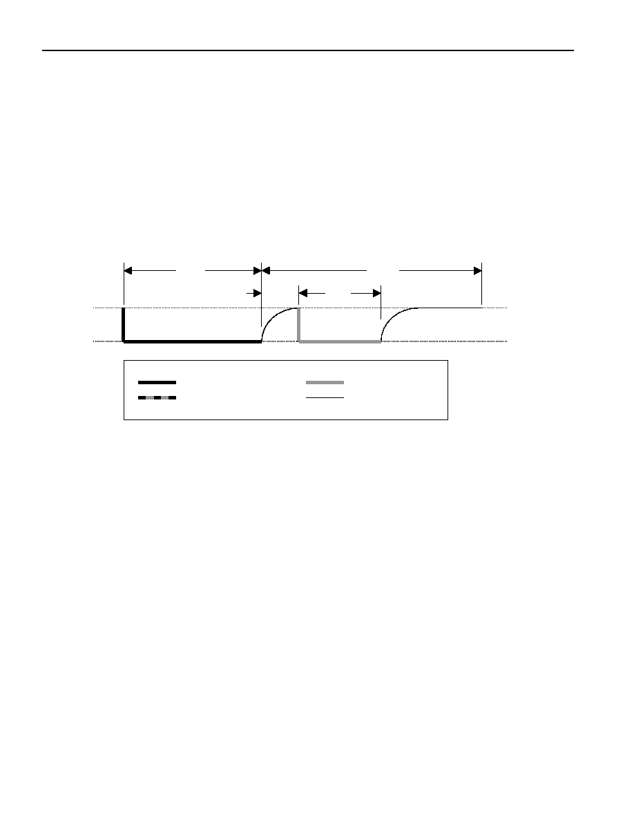
I/O SIGNALING
The 1-Wire bus requires strict signaling protocols to insure data integrity. The four protocols used by the
DS2761 are as follows: the initialization sequence (reset pulse followed by presence pulse), write 0, write
1, and read data. All of these types of signaling except the presence pulse are initiated by the bus master.
The initialization sequence required to begin any communication with the DS2761 is shown in Figure 17.
A presence pulse following a reset pulse indicates that the DS2761 is ready to accept a net address
command. The bus master transmits (Tx) a reset pulse for t
RSTL
. The bus master then releases the line and
goes into receive mode (Rx). The 1-Wire bus line is then pulled high by the pullup resistor. After
detecting the rising edge on the DQ pin, the DS2761 waits for t
PDH
and then transmits the presence pulse
for t
PDL
.
Figure 17. 1-WIRE INITIALIZATION SEQUENCE
WRITE-TIME SLOTS
A write-time slot is initiated when the bus master pulls the 1-Wire bus from a logic-high (inactive) level
to a logic-low level. There are two types of write-time slots: write 1 and write 0. All write-time slots must
be t
SLOT
(60
m
s to 120
m
s) in duration with a 1
m
s minimum recovery time, t
REC
, between cycles. The
DS2761 samples the 1-Wire bus line between 15
m
s and 60
m
s after the line falls. If the line is high when
sampled, a write 1 occurs. If the line is low when sampled, a write 0 occurs (see Figure 18). For the bus
master to generate a write 1 time slot, the bus line must be pulled low and then released, allowing the line
to be pulled high within 15
m
s after the start of the write time slot. For the host to generate a write 0 time
slot, the bus line must be pulled low and held low for the duration of the write-time slot.
READ-TIME SLOTS
A read-time slot is initiated when the bus master pulls the 1-Wire bus line from a logic-high level to a
logic-low level. The bus master must keep the bus line low for at least 1
m
s and then release it to allow the
DS2761 to present valid data. The bus master can then sample the data t
RDV
(15
m
s) from the start of the
read-time slot. By the end of the read-time slot, the DS2761 releases the bus line and allows it to be
pulled high by the external pullup resistor. All read-time slots must be t
SLOT
(60
m
s to 120
m
s) in duration
with a 1
m
s minimum recovery time, t
REC
, between cycles. See Figure 18 for more information.
t
RSTL
t
PDL
t
RSTH
t
PDH
PACK+
PACK-
LINE TYPE LEGEND:
BUS MASTER ACTIVE LOW
DS2761 ACTIVE LOW
RESISTOR PULLUP
BOTH BUS MASTER AND
DS2761 ACTIVE LOW
DQ
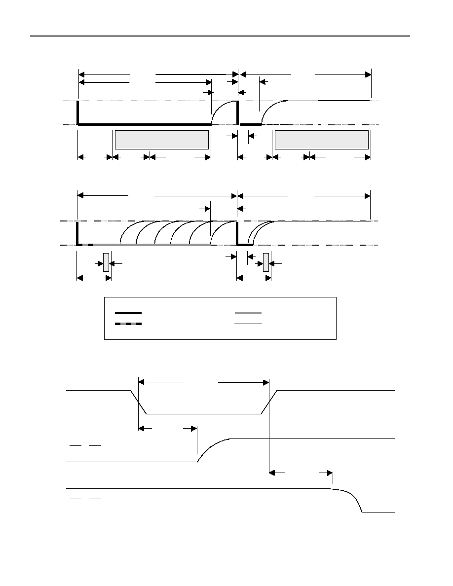
DS2761
21 of 24
Figure 18. 1-WIRE WRITE- AND READ-TIME SLOTS
Figure 19. SWAP COMMAND TIMING
PACK+
PACK-
t
SLOT
DQ
t
LOW1
t
SLOT
WRITE 0 SLOT
WRITE 1 SLOT
t
LOW0
t
REC
>1
ms
DS2761 SAMPLE WINDOW
MIN
TYP
MAX
15
ms
15
ms
30
ms
DS2761 SAMPLE WINDOW
MIN
TYP
MAX
15
ms
15
ms
30
ms
LINE TYPE LEGEND:
BUS MASTER ACTIVE LOW
DS2761 ACTIVE LOW
RESISTOR PULLUP
BOTH BUS MASTER AND
DS2761 ACTIVE LOW
t
SLOT
READ 0 SLOT
READ 1 SLOT
t
SLOT
t
REC
>1
ms
t
RDV
MASTER SAMPLE WINDOW
MASTER SAMPLE WINDOW
t
RDV
PACK+
PACKÙ
DQ
t
SWOFF
t
SWON
t
SWL
CC , DC
CC , DC
DQ
DS2761
22 of 24
ABSOLUTE MAXIMUM RATINGS*
Voltage on PLS and CC Pin, Relative to V
SS
-0.3V to +18V
Voltage on PIO Pin, Relative to V
SS
-0.3V to +12V
Voltage on VIN and
PS, Relative to V
SS
-0.3V to V
DD
+ 0.3
Voltage on any Other Pin, Relative to V
SS
-0.3V to +6V
Continuous Internal Sense Resistor Current
Ý2.5A
Pulsed Internal Sense Resistor Current
Ý50A for <100çs/sec, <1000 pulses
Operating Temperature Range
-40¯C to +85¯C
Storage Temperature Range
-55¯C to +125¯C
Soldering Temperature
See IPC/JEDECJ-STD-020A
* This is a stress rating only and functional operation of the device at these or any other conditions above
those indicated in the operation sections of this specification is not implied. Exposure to absolute
maximum rating conditions for extended periods of time may affect reliability.
RECOMMENDED DC
OPERATING CONDITIONS
(-20
¯C to +70¯C, 2.5V È V
DD
È 5.5V)
PARAMETER
SYMBOL
CONDITIONS
MIN
TYP
MAX
UNITS
NOTES
Supply Voltage
V
DD
2.5
5.5
V
1
Data Pin
DQ
-0.3
+5.5
V
1
DC ELECTRICAL CHARACTERISTICS
(-20
¯C to +70¯C, 2.5V È V
DD
È 5.5V)
PARAMETER
SYMBOL CONDITIONS
MIN
TYP
MAX
UNITS NOTES
Active Current
I
ACTIVE
DQ = V
DD
,
norm. operation
60
90
mA
Sleep Mode Current
I
SLEEP
DQ = 0V,
no activity,
PS
floating
1
2
mA
Input Logic High:
DQ, PIO
V
IH
1.5
V
1
Input Logic High:
PS
V
IH
V
DD
-
0.2V
V
1
Input Logic Low:
DQ, PIO
V
IL
0.4
V
1
Input Logic Low:
PS
V
IL
0.2
V
1
Output Logic High:
CC
V
OH
I
OH
= -0.1mA
V
PLS
-
0.4V
V
1
Output Logic High:
DC
V
OH
I
OH
= -0.1mA
V
DD
-
0.4V
V
1
Output Logic Low:
CC , DC
V
OL
I
OL
= 0.1mA
0.4
V
1
Output Logic Low:
DQ, PIO
V
OL
I
OL
= 4mA
0.4
V
1
DQ Pulldown Current
I
PD
1
mA
Input Resistance: V
IN
R
IN
5
M
W
Internal Current-Sense
Resistor
R
SNS
+25
¯C
20
25
30
m
W
DQ Low to Sleep time
t
SLEEP
2.1
s
DS2761
23 of 24
ELECTRICAL CHARACTERISTICS:
PROTECTION CIRCUITRY
(0
¯C to +50¯C, 2.5V È V
DD
È 5.5V)
PARAMETER
SYMBOL
MIN
TYP
MAX
UNITS
NOTES
Overvoltage Detect
V
OV
4.325
4.250
4.350
4.275
4.375
4.300
V
1, 2
Charge Enable
V
CE
4.10
4.15
4.20
V
1
Undervoltage Detect
V
UV
2.5
2.6
2.7
V
1
Overcurrent Detect
I
OC
1.8
1.9
2.0
A
3
Overcurrent Detect
V
OC
45
47.5
50
mV
1, 4
Short-Circuit Detect
I
SC
5.0
8.0
11
A
3
Short-Circuit Detect
V
SC
150
200
250
mV
1
Overvoltage Delay
t
OVD
0.8
1
1.2
sec
Undervoltage Delay
t
UVD
90
100
110
ms
Overcurrent Delay
t
OCD
5
10
20
ms
Short-Circuit Delay
t
SCD
80
100
120
m
s
Test Threshold
V
TP
0.5
1.0
1.5
V
Test Current
I
TST
10
20
40
mA
Recovery Charge Current
I
RC
0.5
1
2
mA
13
ELECTRICAL CHARACTERISTICS:
TEMPERATURE, VOLTAGE, CURRENT
(-20
¯C to +50¯C, 2.5V È V
DD
È 5.5V)
PARAMETER
SYMBOL
MIN
TYP
MAX
UNITS
NOTES
Temperature Resolution
T
LSB
0.125
¯C
Temperature Full-Scale
Magnitude
T
FS
127
¯C
Temperature Error
T
ERR
Ý3
¯C
5
Voltage Resolution
V
LSB
4.88
mV
Voltage Full-Scale
Magnitude
V
FS
4.75
V
Voltage Offset Error
V
OERR
1
LSB
6
Voltage Gain Error
V
GERR
5
%
Current Resolution
I
LSB
0.625
15.625
mA
m
V
3
4
Current Full-Scale
Magnitude
I
FS
1.9
2.56
64
A
mV
3, 4
7
Current Offset Error
I
OERR
1
LSB
8
Current Gain Error
I
GERR
3
1
%
3, 9
4
Accumulated Current
Resolution
q
CA
0.25
6.25
mAhr
çVhr
3
4
Current Sampling
Frequency
f
SAMP
1456
Hz
Internal Timebase Accuracy
t
ERR
Ý1
Ý3
%
10
DS2761
24 of 24
ELECTRICAL CHARACTERISTICS:
1-WIRE INTERFACE
(-20
¯C to +70¯C, 2.5V È V
DD
È 5.5V)
PARAMETER
SYMBOL
MIN
TYP
MAX
UNITS
NOTES
Time Slot
t
SLOT
60
120
m
s
Recovery Time
t
REC
1
m
s
Write 0 Low Time
t
LOW0
60
120
m
s
Write 1 Low Time
t
LOW1
1
15
m
s
Read Data Valid
t
RDV
15
m
s
Reset Time High
t
RSTH
480
m
s
Reset Time Low
t
RSTL
480
960
m
s
Presence Detect High
t
PDH
15
60
m
s
Presence Detect Low
t
PDL
60
240
m
s
SWAP Timing Pulse Width
t
SWL
0.2
120
m
s
SWAP Timing Pulse Falling
Edge to DC Release
t
SWOFF
0
1
ms
12
SWAP Timing Pulse Rising Edge
to DC Engage
t
SWON
0
1
ms
12
DQ Capacitance
C
DQ
60
pF
EEPROM RELIABILITY SPECIFICATION
(-20
¯C to +70¯C, 2.5V È V
DD
È 5.5V)
PARAMETER
SYMBOL
MIN
TYP
MAX
UNITS
NOTES
Copy to EEPROM Time
t
EEC
2
10
ms
EEPROM Copy Endurance
N
EEC
25000
cycles
11
NOTES
1) All voltages are referenced to V
SS
.
2) See the Ordering Information section to determine the corresponding part number for each V
OV
value.
3) Internal current-sense resistor configuration.
4) External current-sense resistor configuration.
5) Self-heating due to output pin loading and sense resistor power dissipation can alter the reading from
ambient conditions.
6) Voltage offset measurement is with respect to V
OV
at +25¯C.
7) The current register supports measurement magnitudes up to 2.56A using the internal sense resistor
option and 64mV with the external resistor option. Compensation of the internal sense resistor value
for process and temperature variation can reduce the maximum reportable magnitude to 1.9A.
8) Current offset error null to Ý1LSB typically requires 3.5s in-system calibration by user.
9) Current gain error specification applies to gain error in converting the voltage difference at IS1 and
IS2, and excludes any error remaining after the DS2761 compensates for the internal sense resistor's
temperature coefficient of 3700ppm/
¯C to an accuracy of Ý500ppm/¯C. The DS2761 does not
compensate for external sense resistor characteristics, and any error terms arising from the use of an
external sense resistor should be taken into account when calculating total current measurement error.
10) Typical value for t
ERR
is at 3.6V and +25
¯C.
11) Four year data retention at +70
¯C.
12) Typical load capacitance on DC and CC is 1000pF.
13)
Test conditions are PLS = 4.1V, V
DD
= 2.5V. Maximum current for conditions of PLS = 15V,
V
DD
= 0V is 10mA.