/home/web/htmldatasheet/html/maxim/170435
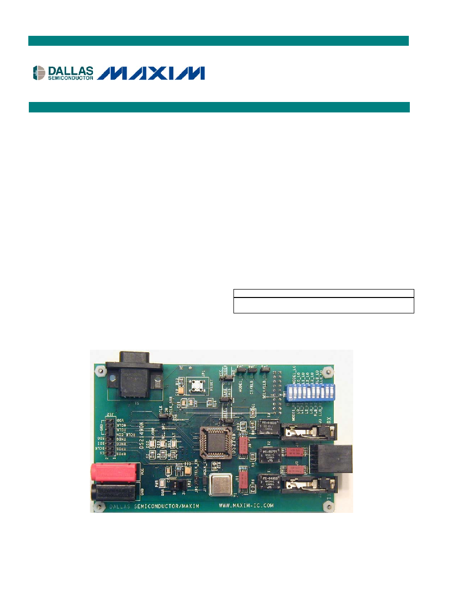
1 of 14
REV: 032403
GENERAL DESCRIPTION
The DS2149DK/DS21349DK is a fully integrated
design kit for the DS2149 and the DS21349 T1/J1
line interface units (LIUs). It contains the necessary
circuitry to evaluate the device in all operation
modes, including running the device in hardware and
software mode.
DESIGN KIT CONTENTS
DS2149DK/DS21349DK Board
DS2149 28-Pin PLCC
DS21349 28-Pin PLCC
FEATURES
§
PLCC 28-Pin Socket for Multiple Part Evaluation
§
Bantam and RJ48 Connectors, Transformers,
and Termination Passives for LIU
§
Two Separate and Controllable Transmit Paths
for TTIP and TRING for Evaluating Multiple
Transformers
§
Equipment-Side Connector for External Data
Source/Sink or External Remote Loopback
§
On-Board T1 Crystal Oscillator
§
On-Board 8051 Microprocessor for Software
Mode Access
§
Connector Accesses to CS, SCLK, SDI, and
SDO for Firmware Development
§
Controllable 5V and 3.3V for VCC and IO Pins to
Support the DS2149 and DS21349 LIUs
ORDERING INFORMATION
PART DESCRIPTION
DS2149DK/
DS21349DK
T1/J1 Line Interface Unit Design Kit
DS2149DK/DS21349DK
T1/J1 Line Interface Unit
Design Kit
www.maxim-ic.com

DS2149DK/DS21349DK T1/J1 Line Interface Unit Design Kit
2 of 14
COMPONENT LIST
DESIGNATION QTY
DESCRIPTION
SUPPLIER
PART
C1 1
0.001
mF capacitor (SMT80123)
Digi-Key --
C3, C6, C9, C12,
C15C17, C19
8
10
mF capacitors (SMT80123)
Digi-Key --
C4, C7, C10, C21
4
0.1
mF capacitors (SMT80123)
Digi-Key --
C5, C8, C11, C22,
C23
5
0.01
mF capacitors (SMT80123)
Digi-Key --
C13, C14
2
10
mF capacitors (SMT127240)
Digi-Key --
C18, C20
2
22pF capacitors (SMT80123)
Digi-Key
--
DS1DS3, DS5
4
Red LED
Digi-Key
LN1251C
DS7
1
150-mil SO, DS87C520-ECL
Dallas Semiconductor
DS87C520-ECL
J1
1
Connector, RJ48, 8-pin
Digi-Key
15-43-8588
J2, J3
2
Bantam connectors
Digi-Key
RTT34B02
J4J11 8
COTO9802
Coto
Technology COTO9802
J12 1
100-mil, 16-pin vertical
connector
Digi-Key --
JP1 1
Pushbutton
switch
Digi-Key
EVQPAE04M
JP2JP6
5
100-mil SIP jumper 2 position
Digi-Key
--
JP7JP10
4
100-mil SIP jumper 3 position
Digi-Key
--
PWR_CONNBAN2
1
Banana connector, 2-pin, red
Mouser Electronics
164-6219
PWR_CONNBAN1
1
Banana connector, 2-pin, black
Mouser Electronics
164-6218
R1R3, R12, R14
5
300
W resistors (SMT80123)
Digi-Key --
R4, R5
2
4.7
W resistors (SMT80123)
Digi-Key --
R6, R7, R10, R11
4
0
W resistors (SMT80123)
Digi-Key --
R8, R9
2
50.0
W resistors (SMT80123)
Digi-Key --
R13, R15, R16
3
10.0k
W resistors SMT80123)
Digi-Key --
R17R21 5
30
W resistors (SMT80123)
Digi-Key --
RN1, RN2
2
1k
W 10-pin resistor network
Digi-Key --
S1 1
9-pin
DB9P
connector Digi-Key
747459-1
SW1 1
10-position
switch
Digi-Key
435668-9
SW2
1
6-pin DPDT switch
Digi-Key
SSA22
T1 1
1:3
T1
transformer Pulse
Engineering
PE-64933
T2 1
1:2
T1
transformer Pulse
Engineering
PE-65771
T3 1
1:1
T1
transformer Pulse
Engineering
PE-64936
U1 1
PLCCSMT28T0T
socket
Pioneer Electronics
PLCCSMT28T0T
U2, U5, U7
3
150-mil SO, 74HC04, hex
inverter
Digi-Key TC74HC04AFN
U3, U4, U6
3
150-mil SO, 74HC03, open
collector NAND gate
Digi-Key SN74LS38D
U8
1
Darlington array
Texas Instruments
ULQ2003ADR
U9
1
150-mil SO, DS232AR
Dallas Semiconductor
DS232AR
U10 1
3.3V
regulator
Maxim
MAX8887EZK33
X1
1
EC1-S-11.0592M XTAL low pro
Digi-Key
EC1-S-11.0592M
Y1
1
1.544MHz crystal oscillator
Digi-Key
NTH039A3-1.5440
DS2149DK/DS21349DK T1/J1 Line Interface Unit Design Kit
3 of 14
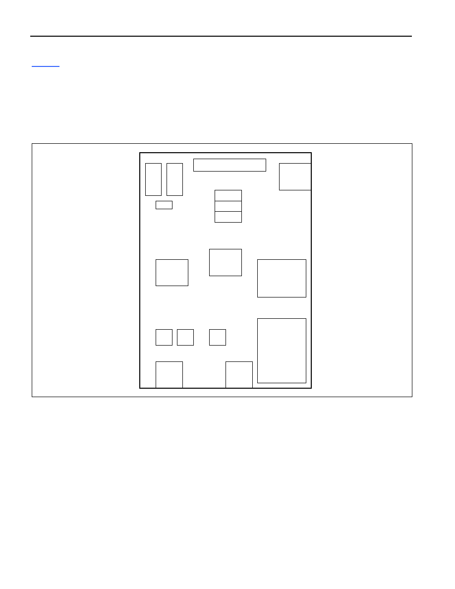
BOARD FLOORPLAN
Figure 1
shows the board layout for the DS2149DK. The DS2149 PLCC socket is in the center of the board. The
line-side bantam connectors for the Tx and Rx differential pairs and transformers are at the bottom of the board,
while the system connector and configuration jumpers are at the top. The LEDs for INT, INLOOP, and RCL/QPD
are in the center of the board, right above the DS2149 socket. The power-supply connectors and power indicator
LED are in the upper left corner of the board, while the DB9 serial connector is the upper left. A T1 oscillator sits to
the left of the DS2149 socket below a switch for changing the voltage to the DS2149 socket from 5V to 3.3V.
Please refer to the general locations on the board when this document references specific items on the DS2149DK.
Figure 1. Board Floorplan
POWER JACKS
SYSTEM CONNECTOR
DS2149
INT
CONFIGURATION
JUMPERS
T1
Tx
Rx
Tx
RCL
NLOOP
Rx
TRANSFORMERS
OSCILLATOR
LINE CONNECTORS
LEDs
VD
D
GND
PWR
LED
SERIAL
PORT
Tx
CONFIGURATION
SWITCHES
Dallas
Semiconductor
DS2149DK/
DS21349DK
DS2149DK/DS21349DK T1/J1 Line Interface Unit Design Kit
4 of 14
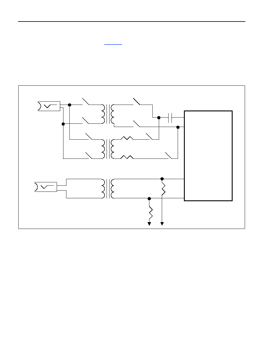
LINE-SIDE CONNECTIONS
The DS2149DK/DS21349DK implements the Tx and Rx line interface networks recommended in the DS2149 and
DS21349 data sheets and as shown in
Figure 2
. To connect the DS2149DK/DS21349DK to T1 or J1 test
equipment, connect the equipment to the RJ48 connector or to the two bantam connectors, J2 and J3. Please
notice the relays disconnecting TTIP and TRING on T1 and T2. These relays disconnect the series resistors R4
and R5, which is recommended for some long-haul configurations. Pin 16 on the system connector serves as the
control line for the relays. When pin 16 is high, T2 is enabled with TTIP and TRING. When it is held low, T1 is
enabled with TTIP and TRING.
Figure 2. Line-Side Circuitry
T3
J3
RECEIVE
R9
50
W
(1%)
R8
50
W
(1%)
RTIP
RRING
Dallas
Semiconductor
DS2149/DS21349
TTIP
TRING
TRANSMIT
J2
T2
T1
C2
1
mF
R4
4.7
W
(1%)
R5
4.7
W
(1%)
DS2149DK/DS21349DK T1/J1 Line Interface Unit Design Kit
5 of 14
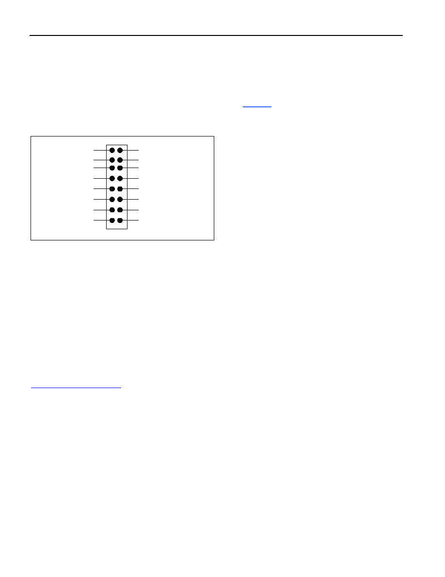
SYSTEM CONNECTOR
A 16-pin system connector at the top of the board gives access to the following signals: RPOS, TPOS, RNEG,
TNEG, RCLK_CON, TCLK, MCLK, V
DD
, GND, CS, SCLK, SDI, and RELAY_CONTROL. By using jumpers to
connect TCLK to RCLK_CON, TPOS to RPOS, and TNEG to RNEG, the system connector can also be used to
implement an external remote loopback. Additionally, the system connector can read and write to the device
without going through the on-board microcontroller. With this feature, you can quickly use this design kit as a
working prototype and begin writing firmware for your system.
Figure 3
shows a representation of the system
connector.
Figure 3. System Connector
POWER-SUPPLY CONNECTORS
Connect a 5.0V power supply across the red (VDD) and black (GND) banana jacks. The red PWR LED indicates
power is applied to the board. Select the appropriate voltage that needs to be applied to VDD from the power
switch below the PWR LED, depending if you are using a DS2149 (5V) or DS21349 (3.3V).
MICROCONTROLER AND SERIAL CONNECTOR
The DS2149DK/DS21349DK contains an on-board 8051 microcontroller with factory-installed firmware loaded into
the microcontroller's EPROM. This firmware translates memory access requests from the RS-232 serial port into
register access to the DS2149 or DS21349 in software mode. DemoView, a software application created by Dallas
Semiconductor, allows easy read-write access for this device.
INSTALLING AND RUNNING THE SOFTWARE
DemoView is a general-purpose program that supports several Dallas Semiconductor design kits. To install the
DemoView software, run SETUP.EXE from the DemoView.ZIP file. (Download DemoView.ZIP from our website,
www.maxim-ic.com/telecom
.) After installation, run the DEMOVIEW.EXE program with the
DS2149DK/DS21349DK board powered up and connected to the PC. In the opening screen, click the REGVIEW
button. Select the correct serial port in the Port Selection dialog box, then click OK. To configure DEMOVIEW to
support the DS2149DK/DS21349DK, open the File pulldown menu and select Definition File. In the Choose
Definition File dialog box, select DS2149DK.DEF and click Open.
After selecting the definition file, the main part of the REGVIEW window displays the DS2149's memory map. To
select a register, click on it in the register map. When a register is selected, the full name of the register and its bit
map are displayed at the bottom of the REGVIEW window. Bits that are logic 0 are displayed in white, while bits
that are logic 1 are displayed in green.
The DemoView software supports the following actions:
§
Toggle a bit. Select the register in the register map and then click the bit in the bit map.
§
Write a register. Select the register, click the Write button, and enter the value to be written.
§
Write all registers. Click the Write All button and enter the value to be written.
§
Read a register. Select the register in the register map and click the Read button.
§
Read all registers. Click the Read All button.
RELAY_CONTROL
CS
SCLK
TPOS
SDI
RPOS
RNEG
SDO
TNEG
GND
RCLK
GND
TCLK
GND
MCLK
VDD