Microsoft Word - DS1992_93-ecn.doc

1 of 16
031003
SPECIAL FEATURES
§ 4096 bits of Read/Write Nonvolatile
Memory (DS1993)
§ 1024 bits of Read/Write Nonvolatile
Memory (DS1992)
§ 256-bit Scratchpad Ensures Integrity of Data
Transfer
§ Memory Partitioned into 256-bit Pages for
Packetizing Data
§ Data Integrity Assured with Strict
Read/Write Protocols
§ Operating Temperature Range from -40°C to
+70°C
§ Over 10 years of data retention
COMMON iButton FEATURES
§ Unique, Factory-Lasered and Tested 64-bit
Registration Number (8-bit Family Code +
48-bit Serial Number + 8-bit CRC Tester)
Assures
Absolute Traceability Because No
Two Parts are
Alike
§ Multidrop Controller for MicroLAN
§ Digital Identification and Information by
Momentary Contact
§ Chip-Based Data Carrier Compactly Stores
Information
§ Data Can be Accessed While Affixed to
Object
§ Economically Communicates to Bus Master
with a Single Digital Signal at 16.3kbps
§ Standard 16mm Diameter and 1-Wire
®
Protocol Ensure Compatibility with iButton
®
Family
§ Button Shape is Self-Aligning with Cup-
Shaped Probes
§ Durable Stainless Steel Case Engraved with
Registration Number Withstands Harsh
Environments
§ Easily Affixed with Self-Stick Adhesive
Backing, Latched by its Flange, or Locked
with a Ring Pressed onto its Rim
§ Presence Detector Acknowledges When
Reader First Applies Voltage
§ Meets UL#913 (4th Edit.); Intrinsically Safe
Apparatus, Approved under Entity Concept
for use in Class I, Division 1, Group A, B, C
and D Locations
F5 MICROCAN
IO
GND
0.36
0.51
5.89
© 1993
YYWW REGISTERED RR
DD
06
000000FBD804
16.25
17.35
All dimensions shown in millimeters.
ORDERING INFORMATION
DS1992L-F5 F5
MicroCan
DS1993L-F5 F5
MicroCan
EXAMPLES OF ACCESSORIES
DS9096P Self-Stick Adhesive Pad
DS9101 Multipurpose Clip
DS9093RA Mounting Lock Ring
DS9093F Snap-In Fob
DS9092 iButton Probe
DS1992/DS1993
1kb/4kb Memory iButton
www.iButton.com
1-Wire and iButton are registered trademarks of Dallas Semiconductor.

DS1992/DS1993
2 of 16
iButton DESCRIPTION
The DS1992/DS1993 memory iButtons (hereafter referred to as DS199_) are rugged read/write data
carriers that act as a localized database, easily accessible with minimal hardware. The nonvolatile
memory and optional timekeeping capability offer a simple solution to storing and retrieving vital
information pertaining to the object to which the iButton is attached. Data is transferred serially through
the 1-Wire protocol that requires only a single data lead and a ground return.
The scratchpad is an additional page that acts as a buffer when writing to memory. Data is first written to
the scratchpad where it can be read back. After the data has been verified, a copy scratchpad command
transfers the data to memory. This process ensures data integrity when modifying the memory. A 48-bit
serial number is factory lasered into each DS199_ to provide a guaranteed unique identity that allows for
absolute traceability. The durable MicroCan package is highly resistant to environmental hazards such as
dirt, moisture, and shock. Its compact coin-shaped profile is self-aligning with mating receptacles,
allowing the DS199_ to be easily used by human operators. Accessories permit the DS199_ to be
mounted on almost any surface including plastic key fobs, photoID badges, and PC boards.
Applications include access control, work-in-progress tracking, electronic travelers, storage of calibration
constants, and debit tokens.
OPERATION
The DS199_ have three main data components: 1) 64-bit lasered ROM, 2) 256-bit scratchpad, and 3)
1024-bit (DS1992) or 4096-bit (DS1993) SRAM. All data is read and written least significant bit first.
The memory functions are not available until the ROM function protocol has been established. This
protocol is described in the ROM functions flow chart (Figure 9). The master must first provide one of
four ROM function commands: 1) read ROM, 2) match ROM, 3) search ROM, or 4) skip ROM. After a
ROM function sequence has been successfully executed, the memory functions are accessible and the
master can then provide any one of the four memory function commands (Figure 6).
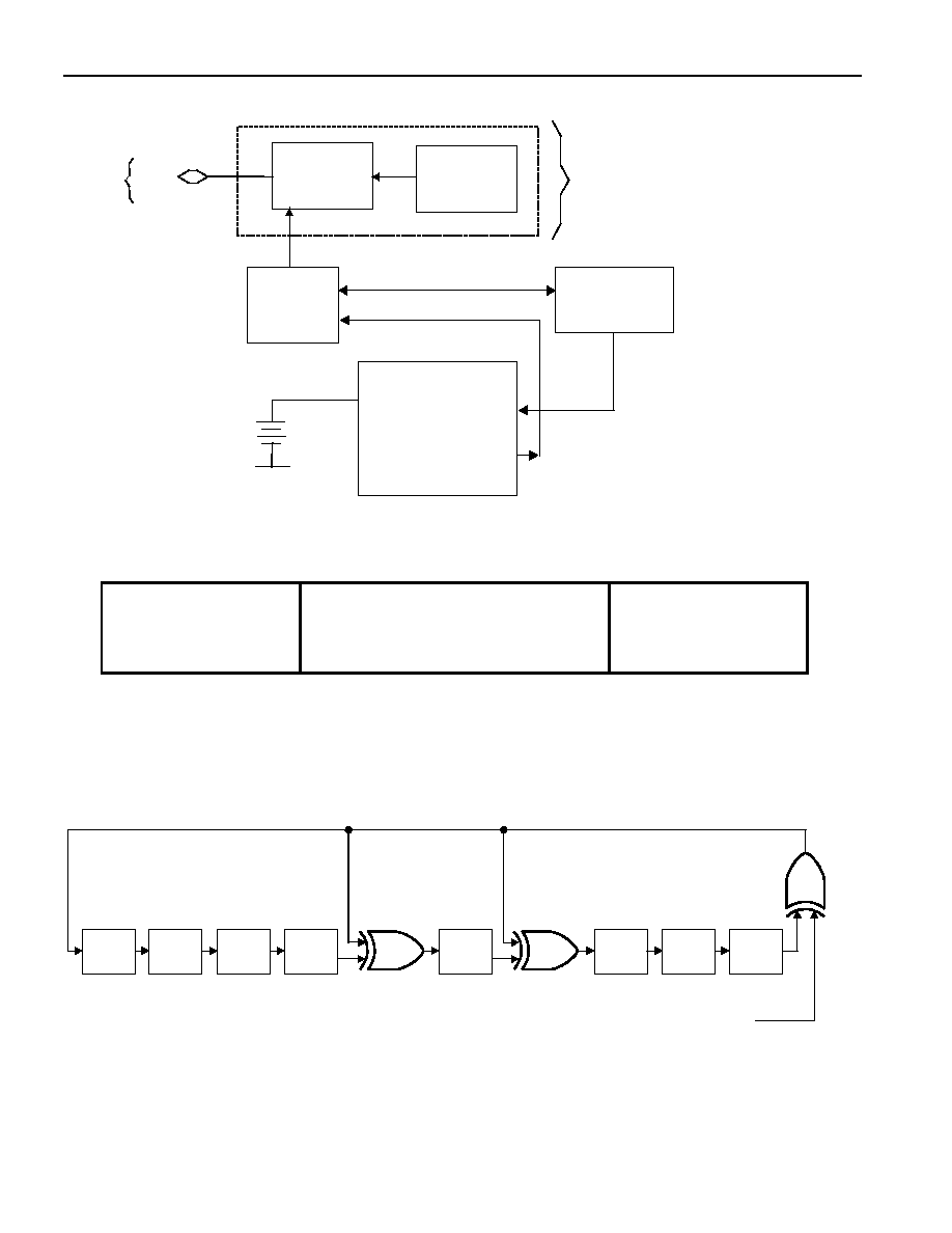
PARASITE POWER
The block diagram (Figure 1) shows the parasite-powered circuitry. This circuitry steals power whenever
the data input is high. The data line provides sufficient power as long as the specified timing and voltage
requirements are met. The advantages of parasite power are two-fold: 1) by parasiting off this input,
lithium is conserved, and 2) if the lithium is exhausted for any reason, the ROM can still be read
normally.
64-bit LASERED ROM
Each DS199_ contain a unique ROM code that is 64 bits long. The first 8 bits are a 1-Wire family code.
The next 48 bits are a unique serial number. The last 8 bits are a CRC of the first 56 bits. (See Figure 2.)
The 1-Wire CRC is generated using a polynomial generator consisting of a shift register and XOR gates
as shown in Figure 3. The polynomial is X
8
+ X
5
+ X
4
+ 1. Additional information about the Dallas 1-Wire
Cyclic Redundancy Check is available in the Book of DS19xx iButton Standards. The shift register bits
are initialized to zero. Then starting with the least significant bit of the family code, 1 bit at a time is
shifted in. After the 8th bit of the family code has been entered, then the serial number is entered. After
the 48th bit of the serial number has been entered, the shift register contains the CRC value. Shifting in
the 8 bits of CRC should return the shift register to all zeros.
DS1992/DS1993
3 of 16
Figure 1. DS199_ BLOCK DIAGRAM
SRAM
16 PAGES of 256-
BITs (1993)
256-BIT
SCRATCHPAD
1-W
ROM
CONTROL
FUNCTION
64-BIT
ROM
LASERED
PARASITE-
CIRCUITRY
POWERED
MEMORY
FUNCTION
CONTROL
1-WIRE
PORT
3V LITHIUM
4 PAGES of 256-
BITs (1992)
Figure 2. 64-BIT LASERED ROM
MSB
LSB
8-Bit CRC Code
48-Bit Serial Number
8-Bit Family Code
(06h)1993
(08h)1992
MSB
LSB MSB
LSB MSB
LSB
Figure 3. 1-WIRE CRC CODE
X
0
X
1
X
2
X
3
X
4
X
5
X
6
X
7
X
8
Polynomial = X
8
+ X
5
+ X
4
+ 1
1
st
STAGE
2
nd
STAGE
3
rd
STAGE
4
th
STAGE
6
th
STAGE
5
th
STAGE
7
th
STAGE
8
th
STAGE
INPUT DATA
DS1992/DS1993
4 of 16
Figure 4a. DS1993 MEMORY MAP
PAGE 0
PAGE
PAGE 1
PAGE 2
PAGE 3
PAGE 4
PAGE 5
PAGE 6
PAGE 7
PAGE 8
PAGE 9
PAGE 10
PAGE 11
PAGE 12
PAGE 13
PAGE 14
PAGE 15
SCRATCHPAD
MEMORY
0000h
0020h
0040h
0060h
0080h
00A0h
00C0h
00E0h
0100h
0120h
0140h
0160h
0180h
01A0h
01C0h
01E0h
NOTE: Each page is 32 bytes (256 bits). The hex values
represent the starting address for each page or register.
Figure 4b. DS1992 MEMORY MAP
PAGE 0
PAGE
PAGE 1
PAGE 2
PAGE 3
SCRATCHPAD
MEMORY
0000h
0020h
0040h
0060h
NOTE: Each page is 32 bytes (256 bits). The hex values
represent the starting address for each page or register.

DS1992/DS1993
5 of 16
MEMORY
The memory map in Figure 4 shows a 32-Byte page called the scratchpad, and additional 32-Byte pages
called memory. The DS1992 contains pages 0 though 3 that make up the 1024-bit SRAM. The DS1993
contain pages 0 through 15 that make up the 4096-bit SRAM.
The scratchpad is an additional page that acts as a buffer when writing to memory. Data is first written to
the scratchpad where it can be read back. After the data has been verified, a copy scratchpad command
transfers the data to memory. This process ensures data integrity when modifying the memory.
MEMORY FUNCTION COMMANDS
The Memory Function Flow Chart (Figure 6) describes the protocols necessary for accessing the memory.
An example follows the flow chart. Three address registers are provided as shown in Figure 5. The first
two registers represent a 16-bit target address (TA1, TA2). The third register is the ending offset/data
status byte (E/S).
The target address points to a unique Byte location in memory. The first 5 bits of the target address
(T4:T0) represent the Byte offset within a page. This Byte offset points to one of 32 possible Byte
locations within a given page. For instance, 00000b points to the first Byte of a page where as 11111b
would point to the last Byte of a page.
The third register (E/S) is a read only register. The first 5 bits (E4: E0) of this register are called the
ending offset. The ending offset is a Byte offset within a page (1 of 32 Bytes). Bit 5 (PF) is the partial
Byte flag. Bit 6 (OF) is the overflow flag. Bit 7 (AA) is the authorization accepted flag.
Figure 5. ADDRESS REGISTERS
7
6
5
4
3
2
1
0
TARGET ADDRESS (TA1)
T7
T6
T5
T4
T3
T2
T1
T0
TARGET ADDRESS (TA2)
T15
T14
T13
T12
T11
T10
T9
T8
ENDING ADDRESS WITH
DATA STATUS (E/S)
(READ ONLY)
AA
OF
PF
E4
E3
E2
E1
E0
Write Scratchpad Command [0Fh]
After issuing the write scratchpad command, the user must first provide the 2-Byte target address,
followed by the data to be written to the scratchpad. The data is written to the scratchpad starting at the
byte offset (T4:T0). The ending offset (E4: E0) is the Byte offset at which the host stops writing data. The
maximum ending offset is 11111b (31d). If the host attempts to write data past this maximum offset, the
overflow flag (OF) is set and the remaining data is ignored. If the user writes an incomplete Byte and an
overflow has not occurred, the partial Byte flag (PF) is set.
Read Scratchpad Command [AAh]
This command can be used to verify scratchpad data and target address. After issuing the read scratchpad
command, the user can begin reading. The first two Bytes are the target address. The next Byte is the
ending offset/data status Byte (E/S) followed by the scratchpad data beginning at the Byte offset (T4: T0).
The user can read data until the end of the scratchpad, after which the data read is all logic 1's.