1 of 40
022703
DS1921L-F5X
Thermochron iButton
www.maxim-ic.com
SPECIAL FEATURES*
§ Digital thermometer measures temperature in
0.5°C increments (accuracy ±1.0
°C)
§ Built-in real-time clock (RTC) and timer has
accuracy of
±2 minutes per month from 0°C
to 45°C
§ Automatically wakes up and measures tem-
perature at user-programmable intervals from
1 to 255 minutes
§ Logs up to 2048 consecutive temperature
measurements in protected nonvolatile (NV)
memory
§ Records a long-term temperature histogram
with 2.0°C resolution
§ Programmable temperature-high and tem-
perature-low alarm trip points
§ Records up to 24 time stamps and durations
when temperature leaves the range specified
by the trip points
§ 512 bytes of general-purpose read/write NV
memory
§ Typical lifetime more than 9 years
§ Communicates to host with a single digital
signal at 14.1kbits or 125kbits per second
using 1-Wire
®
protocol
COMMON iButton FEATURES
§ Digital identification and information by
momentary contact
§ Unique, factory-lasered and tested 64-bit reg-
istration number (8-bit family code + 48-bit
serial number + 8-bit CRC tester) assures ab-
solute traceability because no two parts are
alike
§ Multidrop controller for 1-Wire net
§ Chip-based data carrier compactly stores
information
§ Data can be accessed while affixed to object
§ Button shape is self-aligning with cup-shaped
probes
§ Durable stainless steel case engraved with
registration number withstands harsh envi-
ronments
§ Easily affixed with self-stick adhesive back-
ing, latched by its flange, or locked with a
ring pressed onto its rim
§ Presence detector acknowledges when reader
first applies voltage
§ Meets UL#913 (4th Edit.). Intrinsically Safe
Apparatus: approved under Entity Concept
for use in Class I, Division 1, Group A, B, C
and D Locations (application pending)
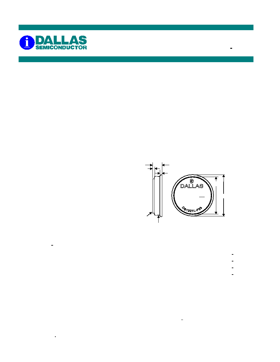
F5 MICROCAN
IO
GND
0.36
0.51
5.89
© 1993
YYWW REGISTERED RR
xx
21
15C000FBC52B
16.25
17.35
All dimensions are shown in millimeters.
ORDERING INFORMATION
DS1921L-F51
-10
°C to +85°C
F5 iButton
®
DS1921L-F52
-20
°C to +85°C
F5 iButton
DS1921L-F53
-30
°C to +85°C
F5 iButton
DS1921L-F50
-40
°C to +85°C
F5 iButton
EXAMPLES OF ACCESSORIES
DS9096P
Self-Stick Adhesive Pad
DS9101
Multi-Purpose Clip
DS9093RA
Mounting Lock Ring
DS9093A
Snap-In Fob
DS9092
iButton Probe
1-Wire, Microcan, and iButton are registered trademarks of Dallas Semiconductor
*See ELECTRICAL CHARACTERISTICS table for details.

DS1921L
2 of 40
iButton DESCRIPTION
The DS1921L Thermochron iButtons are rugged, self-sufficient systems that measure temperature and
record the result in a protected memory section. The recording is done at a user-defined rate, both as a
direct storage of temperature values as well as in the form of a histogram. Up to 2048 temperature values
taken at equidistant intervals ranging from 1 to 255 minutes can be stored. The histogram provides 63
data bins for a resolution of 2.0°C. If the temperature leaves a user-programmable range, the DS1921L
will also record when this happened, for how long the temperature stayed outside the permitted range,
and if the temperature was too high or too low. An additional 512 bytes of read/write NV memory allow
storing information pertaining to the object to which the DS1921L is associated. Data is transferred
serially via the 1-Wire protocol, which requires only a single data lead and a ground return. Every
DS1921L is factory-lasered with a guaranteed unique 64-bit registration number that allows for absolute
traceability. The durable stainless steel package is highly resistant to environmental hazards such as dirt,
moisture, and shock. Accessories permit the DS1921L to be mounted on almost any object, including
containers, pallets, and bags.
APPLICATION
The DS1921L Thermochron iButton is an ideal device to monitor the temperature of any object it is
attached to or shipped with, such as perishable goods or containers of temperature sensitive chemicals.
Using TMEX, the read/write NV memory can store an electronic copy of shipping information, date of
manufacture and other important data written as clear as well as encrypted files.
OVERVIEW
The block diagram in Figure 1 shows the relationships between the major control and memory sections of
the DS1921L. The device has seven main data components: 1) 64-bit lasered ROM, 2) 256-bit scratch-
pad, 3) 4096-bit general-purpose SRAM, 4) 256-bit register page of timekeeping, control, and counter
registers, 5) 96 bytes of alarm time stamp and duration logging memory, 6) 126 bytes of histogram mem-
ory, and 7) 2048 bytes of data-logging memory. Except for the ROM and the scratchpad, all other mem-
ory is arranged in a single linear address space. All memory reserved for logging purposes, counter reg-
isters and several other registers are read-only for the user. The timekeeping and control registers are
write-protected while the device is programmed for a mission.
The hierarchical structure of the 1-Wire protocol is shown in Figure 2. The bus master must first provide
one of the seven ROM function commands: 1) Read ROM, 2) Match ROM, 3) Search ROM, 4) Condi-
tional Search ROM, 5) Skip ROM, 6) Overdrive-Skip ROM or 7) Overdrive-Match ROM. Upon comple-
tion of an Overdrive ROM command byte executed at standard speed, the device will enter Overdrive
mode, where all subsequent communication occurs at a higher speed. The protocol required for these
ROM function commands is described in Figure 12. After a ROM function command is successfully exe-
cuted, the memory functions become accessible and the master may provide any one of the seven avail-
able commands. The protocol for these memory function commands is described in Figure 10. All data is
read and written least significant bit first.

DS1921L
3 of 40
DS1921L BLOCK DIAGRAM Figure 1
Internal
Timekeeping &
Control Reg. &
Counters
3V Lithium
General-Purpose
SRAM
Register Page
Alarm Time Stamp
and Duration
Logging Memory
Datalog
Memory
Histogram Memory
32.768kHz
Oscillator
Control
Logic
Temperature
Sensor
256-Bit
Scratchpad
Memory
Function
Control
ROM
Function
Control
64-Bit
Lasered
ROM
Parasite
Powered
Circuitry
1-Wire
Port
IO
PARASITE POWER
The block diagram (Figure 1) shows the parasite-powered circuitry. This circuitry "steals" power when-
ever the IO input is high. IO will provide sufficient power as long as the specified timing and voltage re-
quirements are met. The advantages of parasite power are two-fold: 1) by parasiting off this input, lithium
is conserved, and 2) if the lithium is exhausted for any reason, the ROM may still be read normally.
64-BIT LASERED ROM
Each DS1921L contains a unique ROM code that is 64 bits long. The first 8 bits are a 1-Wire family
code. The next 36 bits are a unique serial number. The next 12 bits, called temperature range code, allow
distinguishing the various DS1921L-F5 versions from each other and from the DS1921H and DS1921Z.
The last eight bits are a CRC of the first 56 bits. See Figure 3 for details. The 1-Wire CRC is generated
using a polynomial generator consisting of a shift register and XOR gates as shown in Figure 4. The
polynomial is X
8
+ X
5
+ X
4
+ 1. Additional information about the Dallas 1-Wire Cyclic Redundancy
Check is available in Application Note 27 and in the Book of DS19xx iButton Standards.
The shift register bits are initialized to 0. Then starting with the least significant bit of the family code,
one bit at a time is shifted in. After the eighth
bit of the family code has been entered, then the serial
number followed by the temperature range code is entered. After the range code has been entered, the
shift register contains the CRC value. Shifting in the eight bits of CRC returns the shift register to all 0s.

DS1921L
4 of 40
HIERARCHICAL STRUCTURE FOR 1-Wire PROTOCOL Figure 2
1-Wire net
Other
Devices
BUS
Master
Command
Level:
1-Wire ROM Function
Commands
DS1921-specific
Memory Function
Commands
DS1921
Available
Commands:
Read ROM
Match ROM
Search ROM
Skip ROM
Overdrive Skip
Overdrive Match
Conditional Search
ROM
Write Scratchpad
Read Scratchpad
Copy Scratchpad
Read Memory
Read Memory w/CRC
Clear Memory
Convert Temperature
Data Field
Affected:
64-bit Reg. #
64-bit Reg. #
64-bit Reg. #
N/A
OD-Flag
64-bit Reg. #, OD-Flag
64-bit Reg. #, Cond. Search settings,
device status
256-bit scratchpad, flags
256-bit scratchpad
4096-bit SRAM, registers, flags
All memory
All memory
Mission Time Stamp, Mission Samples
Counter, Start Delay, Sample
Rate, Alarm Time Stamps and
Durations, Histogram Memory
Memory address 211h
Cmd.
Codes:
33h
55h
F0h
CCh
3Ch
69h
ECh
0Fh
AAh
55h
F0h
A5h
3Ch
44h
64-BIT LASERED ROM Figure 3
MSB
LSB
8-Bit
CRC Code
12-Bit Temperature
Range Code
36-Bit Serial Number
8-Bit Family
Code (21h)
MSB
LSB
MSB
LSB
MSB LSB
MSB
LSB
DEVICE
TEMP.
RANGE (°C)
RESOLUTION
(
°C)
TEMP. RANGE CODE
HEX.
EQUIVALENT
DS1921L-F51
-10 to +85
0.5
0011
0100
1100
34C
DS1921L-F52
-20 to +85
0.5
0010
0101
0100
254
DS1921L-F53
-30 to +85
0.5
0001
0101
1100
15C
DS1921L-F50
-40 to +85
0.5
0000
0110
0100
064
DS1921H-F5
+15 to +46
0.125
0100
1111
0010
4F2
DS1921Z-F5
-5 to +26
0.125
0011
1011
0010
3B2

DS1921L
5 of 40
1-Wire CRC GENERATOR Figure 4
X
0
X
1
X
2
X
3
X
4
X
5
X
6
X
7
X
8
Polynomial = X
8
+ X
5
+ X
4
+ 1
1
st
STAGE
2
nd
STAGE
3
rd
STAGE
4
th
STAGE
6
th
STAGE
5
th
STAGE
7
th
STAGE
8
th
STAGE
INPUT DATA
MEMORY
The memory map of the DS1921L is shown in Figure 5. The 4096-bit general-purpose SRAM make up
pages 0 through 15. The timekeeping, control, and counter registers fill page 16, called Register Page (see
Figure 6). Pages 17 to 19 are assigned to storing the alarm time stamps and durations. The temperature
histogram bins begin at page 64 and use up to four pages. The temperature logging memory covers pages
128 to 191. Memory pages 20 to 63, 68 to 127, and 192 to 255 are reserved for future extensions. The
scratchpad is an additional page that acts as a buffer when writing to the SRAM memory or the register
page. The memory pages 17 and higher are read-only for the user. They are written to or erased solely
under supervision of the on-chip control logic.
DS1921L MEMORY MAP Figure 5
32-Byte Intermediate Storage Scratchpad
ADDRESS
0000h to
01FFh
General-Purpose SRAM (16 Pages)
Pages 0 to 15
0200h to
021Fh
32-Byte Register Page
Page 16
0220h to
027Fh
Alarm Time Stamps and Durations
Pages 17 to 19
0280h to
07FFh
(Reserved for Future Extensions)
Pages 20 to 63
0800h to
087Fh
Temperature Histogram Memory
Pages 64 to 67
0880h to
0FFFh
(Reserved for Future Extensions)
Pages 68 to 127
1000h to
17FFh
Datalog Memory (64 Pages)
Pages 128 to 191
1800h to
1FFFh
(Reserved for Future Extensions)
Pages 192 to 255