1 of 24
041502
Note: Some revisions of this device may incorporate deviations from published specifications known as errata. Multiple
revisions of any device may be simultaneously available through various sales channels. For information about device errata,
click here:
http://dbserv.maxim-ic.com/errata.cfm
.
FEATURES
§ BCD-coded century, year, month, date, day,
hours, minutes, and seconds with automatic
leap-year compensation valid up to the year
2100
§ Programmable watchdog timer and real-time
clock (RTC) alarm
§ Century register; Y2K-compliant RTC
§ Automatic battery backup and write
protection to external SRAM
§ +5V operation
§ Precision power-on reset
§ Power-control circuitry supports system
power-on from date/day/time alarm or key
closure
§ 256 bytes user NV RAM
§ Auxiliary battery input
§ Accuracy is better than ±1 minute/month at
+25°C
§ Day of week/date alarm register
§ Battery voltage-level indicator flags
§ Optional industrial temperature range:
-40
°
C to +85
°
C
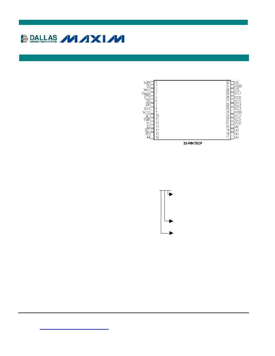
PIN ASSIGNMENT
ORDERING INFORMATION
DS1500XXX
blank Commercial Temp. Range
N
Industrial Temp. Range
E
32-Pin TSOP
Y
5V Operation
Package dimension information can be found at:
http://dbserv.maxim-ic.com/products.cfm
DS1500
Y2KC Watchdog RTC with NV Control
www.maxim-ic.com

DS1500
2 of 24
PIN DESCRIPTION
V
CCI
- Supply Voltage
A0 to A4
- Address Inputs
DQ0 to DQ7 - Data I/O
CS
- RTC Chip-Select Input
OE
- RTC Output-Enable Input
WE
- RTC Write-Enable Input
IRQ
- Interrupt Output (Open Drain)
PWR
- Power-On Output (Open Drain)
RST
- Reset Output (Open Drain)
KS
- Kickstart Input
SQW
- Square-Wave Output
V
BAT
- Backup-Battery Supply
V
BAUX
- Auxiliary-Battery Supply
CEI
- RAM Chip-Enable Input
CEO
- RAM Chip-Enable Output
V
CCO
- RAM Power-Supply Output
X1, X2
- 32.768kHz Crystal Pins
GND
-
Ground
DESCRIPTION
The DS1500 is a full-function, year 2000-compliant real-time clock/calendar (RTC) with an alarm,
watchdog timer, power-on reset, battery monitors, 256 bytes of on-board NV SRAM, NV control for
backing up an external SRAM, and a 32.768kHz output. User access to all registers within the DS1500 is
accomplished with a bytewide interface as shown in Figure 1. The RTC registers contain century, year,
month, date, day, hours, minutes, and seconds data in 24-hour binary-coded decimal (BCD) format.
Corrections for day of month and leap year are made automatically.
The RTC registers are double-buffered into an internal and external set. The user has direct access to the
external set. Clock/calendar updates to the external set of registers can be disabled and enabled to allow
the user to access static data. When the crystal oscillator is turned on, the internal set of registers are
continuously updated; this occurs regardless of external register settings to guarantee that accurate RTC
information is always maintained.
The DS1500 contains its own power-fail circuitry that automatically deselects the device when the V
CCI
supply falls below a power-fail trip point. This feature provides a high degree of data security during
unpredictable system operation caused by low V
CCI
levels. An external SRAM can be made nonvolatile
by using the V
CCO
and
CEO
pins. Nonvolatile control of the external SRAM is analogous to that of the
RTC registers. When V
CCI
slews down during a power fail,
CEO
is driven to an inactive level regardless
of
CEI
. This write protection occurs when V
CCI
is less than the power-fail trip point.
The DS1500 has interrupt (
IRQ
), power control (
PWR
), and reset (
RST
) outputs that can be used to control
CPU activity. The
IRQ
interrupt or
RST
outputs can be invoked as the result of a time-of-day alarm, CPU
watchdog alarm, or a kickstart signal. The DS1500 power-control circuitry allows the system to be
powered on by an external stimulus, such as a keyboard or by a time and date (wake-up) alarm. The
PWR
output pin can be triggered by one or either of these events, and can be used to turn on an external power
supply. The
PWR
pin is under software control, so that when a task is complete, the system power can
then be shut down. The DS1500 power-on reset can be used to detect a system power-down or failure and
hold the CPU in a safe reset state until normal power returns and stabilizes; the
RST
output is used for this
function.
The DS1500 is a clock/calendar chip with the features described above. An external crystal and battery
are the only components required to maintain time-of-day and memory status in the absence of power.

DS1500
3 of 24
Figure 1. BLOCK DIAGRAM
V
CCI
Table 1. RTC OPERATING MODES
V
CCI
CS
OE
WE
DQ0DQ7 A0A4
MODE
POWER
V
IH
X X High-Z X
Deselect
Standby
V
IL
X
V
IL
D
IN
A
IN
Write Active
V
IL
V
IL
V
IH
D
OUT
A
IN
Read Active
V
CCI
> V
PF
V
IL
V
IH
V
IH
High-Z
A
IN
Read Active
V
SO
< V
CCI
< V
PF
X X X High-Z X
Deselect CMOS
Standby
V
CCI
<
V
SO
< V
PF
X X X High-Z X
Data
Retention
Battery Current

DS1500
4 of 24
RTC DATA READ MODE
The DS1500 is in the read mode whenever
CS
(chip select) is low and
WE
(write enable) is high. The
device architecture allows ripple-through access to any valid address location. Valid data is available at
the DQ pins within t
AA
(address access) after the last address input is stable, provided that
CS
and
OE
access times are satisfied. If
CS
or
OE
access times are not met, valid data is available at the latter of
chip-enable access (t
CSA
) or at output-enable access time (t
OEA
). The state of the data input/output pins
(DQ) is controlled by
CS
and
OE
. If the outputs are activated before t
AA
, the data lines are driven to an
intermediate state until t
AA
. If the address inputs are changed while
CS
and
OE
remain valid, output data
remains valid for output-data hold time (t
OH
) but then goes indeterminate until the next address access
(Table 1).
RTC DATA WRITE MODE
The DS1500 is in the write mode whenever
WE
and
CS
are in their active state. The start of a write is
referenced to the latter occurring transition of
WE
or
CS
. The addresses must be held valid throughout the
cycle.
CS
or
WE
must return inactive for a minimum of t
WR
prior to the initiation of a subsequent read or
write cycle. Data in must be valid t
DS
prior to the end of the write and remain valid for t
DH
afterward. In a
typical application, the
OE
signal is high during a write cycle. However,
OE
can be active provided that
care is taken with the data bus to avoid bus contention. If
OE
is low prior to a high-to-low transition on
WE
, the data bus can become active with read data defined by the address inputs. A low transition on
WE
then disables the outputs t
WEZ
after
WE
goes active (Table 1).
DATA RETENTION MODE
The 5V device is fully accessible and data can be written and read only when V
CCI
is greater than V
PF
.
However, when V
CCI
falls below the power-fail point V
PF
(point at which write protection occurs), the
internal clock registers and SRAM are blocked from any access. While in the data retention mode, all
inputs are "don't cares" and outputs go to a high-Z state, with the exception of V
CCO
,
CEO
, and the
possible exception of
KS
,
PWR
, SQW, and
RST
. When V
CCI
falls below the greater of V
BAT
or V
BAUX
,
device power is switched from the V
CCI
pin to the greater of V
BAT
or V
BAUX
. RTC operation and external
SRAM data are maintained from the battery until V
CCI
is returned to nominal levels (Table 1).
All control, data, and address signals must be no more than 0.3V above V
CCI
.

DS1500
5 of 24
AUXILIARY BATTERY
The V
BAUX
input is provided to supply power from an auxiliary battery for the DS1500 kickstart and
square-wave output features in the absence of V
CCI
. This power source must be available to use these
auxiliary features when no V
CCI
is applied to the device.
This auxiliary battery can be used as the primary backup power source for maintaining the clock/calendar
and external SRAM. This occurs if the V
BAT
pin is at a lower voltage than V
BAUX
. If the DS1500 is to be
backed-up using a single battery with the auxiliary features enabled, then V
BAUX
should be used and
connected to V
BAT
. If V
BAUX
is not to be used, it should be grounded.
POWER ON RESET
A temperature-compensated comparator circuit monitors the level of V
CCI
. When V
CCI
falls to the power-
fail trip point, the
RST
signal (open drain) is pulled low. When V
CCI
returns to nominal levels, the
RST
signal continues to be pulled low for a period of 40ms to 200ms. The power-on reset function is
independent of the RTC oscillator and therefore operational whether or not the oscillator is enabled.
CLOCK OSCILLATOR CONTROL
The clock oscillator can be stopped at any time. To increase the shelf life of a backup lithium-battery
source, the oscillator can be turned off to minimize current drain from the battery. The
EOSC
bit is used to
control the state of the oscillator, and must be set to a 0 for the oscillator to function.
READING THE CLOCK
When reading the clock and calendar data, it is recommended to halt updates to the external set of double-
buffered RTC registers. This puts the external registers into a static state allowing data to be read without
register values changing during the read process. Normal updates to the internal registers continue while
in this state. External updates are halted when a 0 is written into the read (TE) bit of control register B
(0Fh). As long as a 0 remains in the control register B (TE) bit, updating is halted. After a halt is issued,
the registers reflect the RTC count (day, date, and time) that was current at the moment the halt command
was issued. Normal updates to the external set of registers resume within 1 second after the (TE) bit is set
to a 1.
SETTING THE CLOCK
It is also recommended to halt updates to the external set of double-buffered RTC registers when writing
to the clock. The TE bit should be used as described above before loading the RTC registers with the
desired RTC count (day, date, and time) in 24-hour BCD format. Setting the TE bit to a 1 transfers the
values written to the internal RTC registers and allows normal operation to resume.
CLOCK ACCURACY
A standard 32.768kHz quartz crystal should be directly connected to the DS1500 X1 and X2 oscillator
pins. The crystal selected for use should have a specified load capacitance (C
L
) of either 6pF or 12.5pF,
and the crystal select (CS) bit set accordingly. For more information about crystal selection and crystal
layout considerations, please consult Application Note 58, "Crystal Considerations with Dallas Real-Time