
MRF16006
The RF Line
NPN Silicon
RF Power Transistor
Designed for 28 Volt microwave largesignal, common base, ClassC CW
amplifier applications in the range 1600 1640 MHz.
·
Specified 28 Volt, 1.6 GHz ClassC Characteristics
Output Power = 6 Watts
Minimum Gain = 7.4 dB, @ 6 Watts
Minimum Efficiency = 40% @ 6 Watts
·
Characterized with Series Equivalent LargeSignal Parameters from
1500 MHz to 1700 MHz
·
Silicon Nitride Passivated
·
Gold Metallized, Emitter Ballasted for Long Life and Resistance to
Metal Migration
MAXIMUM RATINGS
(T
J
= 25
°
C unless otherwise noted)
Rating
Symbol
Value
Unit
CollectorEmitter Voltage
V
CES
60
Vdc
EmitterBase Voltage
V
EBO
4.0
Vdc
CollectorCurrent
I
C
1.0
Adc
Total Device Dissipation @ T
C
= 25
°
C
Derate above 25
°
C
P
D
26
0.15
Watts
W/
°
C
Storage Temperature Range
T
stg
65 to +150
°
C
THERMAL CHARACTERISTICS
Thermal Resistance -- Junction to Case (1) (2)
R
JC
6.8
°
C/W
(1) Thermal measurement performed using CW RF operating condition.
(2) Thermal resistance is determined under specified RF operating conditions by infrared measurement techniques.
MRF16006
CASE 395C01, STYLE 2
6.0 WATTS, 1.6 GHz
RF POWER TRANSISTOR
NPN SILICON
1
REV 2
Order this document
by MRF16006/D
SEMICONDUCTOR TECHNICAL DATA

ELECTRICAL CHARACTERISTICS
(T
C
= 25
°
C unless otherwise noted)
Characteristic
Symbol
Min
Typ
Max
Unit
OFF CHARACTERISTICS
CollectorEmitter Breakdown Voltage
(I
C
= 40 mAdc, V
BE
= 0)
V
(BR)CES
55
--
--
Vdc
CollectorBase Breakdown Voltage
(I
C
= 40 mAdc, I
E
= 0)
V
(BR)CBO
55
--
--
Vdc
EmitterBase Breakdown Voltage
(I
E
= 2.5 mAdc, I
C
= 0)
V
(BR)EBO
4.0
--
--
Vdc
Collector Cutoff Current
(VCE = 28 Vdc, V
BE
= 0)
I
CES
--
--
2.5
mAdc
ON CHARACTERISTICS
DC Current Gain
(I
CE
= 0.2 Adc, V
CE
= 5.0 Vdc)
h
FE
20
--
80
--
DYNAMIC CHARACTERISTICS
Output Capacitance
(V
CB
= 28 Vdc, f = 1.0 MHz)
C
ob
11
--
--
pf
FUNCTIONAL TESTS
CommonBase Amplifier Power Gain
(V
CC
= 28 Vdc, P
out
= 6 Watts, f = 1600/1640 MHz)
G
pe
7.4
--
--
dB
Collector Efficiency
(V
CC
= 28 Vdc, P
out
= 6 Watts, f = 1600/1640 MHz)
40
45
--
%
Return Loss
(V
CC
= 28 Vdc, P
out
= 6 Watts, f = 1600/1640 MHz)
I
RL
--
8.0
--
dB
Output Mismatch Stress
(V
CC
= 28 Vdc, P
out
= 6 Watts, f = 1600 MHz, Load
VSWR = 3:1 all phase angles at frequency of test)
No Degradation in Output Power
2
REV 2
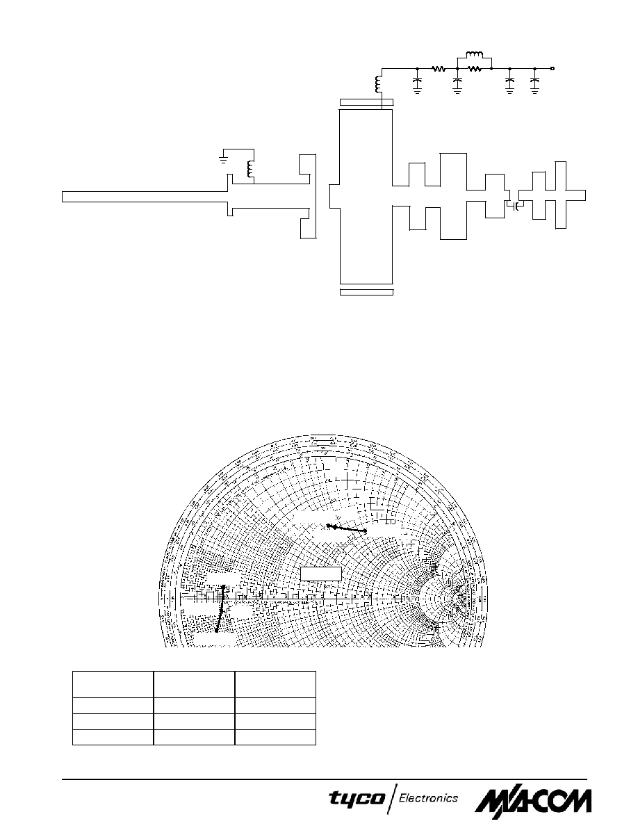
Figure 1. MRF16006 Test Fixture Schematic
L1
L2
B1
C1
C2
C3
C4
L3
R1
28 Vdc
B1
Fair Rite Bead on #24 Wire
C1, C5
100 pF, B Case, ATC Chip Cap
C2
0.1
µ
F, Dipped Mica Cap
C3
0.1
µ
F, Chip Cap
C4
47
µ
F, 50 V, Electrolytic Cap
L1, L2
3 Turns, #18, 0.133
ID, 0.15
Long
L3
9 Turns, #24 Enamel
R1
82
,
1.0 W, Carbon Resistor
Board Material Teflon
®
Glass Laminate Dielectric
Thickness 0.30
,
r
= 2.55
, 2.0 oz. Copper
Figure 2. Series Equivalent Input/Output Impedance
C5
V
CC
= 28 Vdc, P
out
= 6 W
Z
OL
* = Conjugate of the optimum load impedance into which the device
output operates at a given output power, voltage and frequency.
Z
in
Z
OL
*
1.7 GHz
Z
o
= 10
f = 1.5 GHz
1.6 GHz
1.7 GHz
1.6 GHz
f = 1.5 GHz
f
MHz
Z
in
Ohms
Z
OL
*
Ohms
1500
6.28 + j 8.53
1.22 j 1.37
1600
7.04 + j 9.00
1.58 j 0.53
1700
9.55 + j 12.86
1.71 + j 0.39
3
REV 2

Figure 3. Output Power versus Input Power
P
in
, INPUT POWER (WATTS)
12
10
8
6
4
2
0
1.45
1.25
1.05
0.85
0.65
0.45
0.25
P out
, OUTPUT
POWER (W
A
TTS)
f = 1.6 GHz
1.64 GHz
V
CC
= 28 Vdc
4
REV 2

PACKAGE DIMENSIONS
CASE 395C01
ISSUE A
U
D
K
N
J
H
E
C
DIM
A
MIN
MAX
MIN
MAX
MILLIMETERS
0.739
0.750
18.77
19.05
INCHES
B
0.240
0.260
6.10
6.60
C
0.165
0.198
4.19
5.03
D
0.215
0.225
5.46
5.72
E
0.055
0.070
1.40
1.78
H
0.079
0.091
2.01
2.31
J
0.004
0.006
0.10
0.15
K
0.210
0.240
5.33
6.10
N
0.315
0.330
8.00
8.38
Q
0.125
0.135
3.18
3.42
U
0.560 BSC
14.23 BSC
NOTES:
1. DIMENSIONING AND TOLERANCING PER ANSI
Y14.5M, 1982.
2. CONTROLLING DIMENSION: INCH.
SEATING
PLANE
T
1
2
3
A
B
2 PL
Q
M
A
M
0.51 (0.020)
B
M
T
STYLE 2:
PIN 1. EMITTER
2. COLLECTOR
3. BASE
5
Specifications subject to change without notice.
n
North America: Tel. (800) 366-2266, Fax (800) 618-8883
n
Asia/Pacific: Tel.+81-44-844-8296, Fax +81-44-844-8298
n
Europe: Tel. +44 (1344) 869 595, Fax+44 (1344) 300 020
Visit www.macom.com for additional data sheets and product information.
REV 2