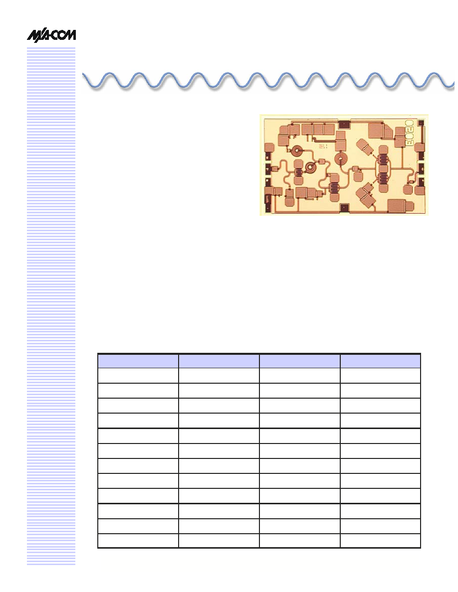
MAAPGM0040-DIE_Ckt_952-7.PUB
0.5W X/Ku-Band Power Amplifier
10.5-15.5 GHz
MAAPGM0040-DIE
10.5-15.5 GHz GaAs MMIC Amplifier
RO-P-DS-3023 - -
Preliminary Information
Features
10.5-15.5 GHz Operation
0.5 Watt Saturated Output Power Level
Variable Drain Voltage (4-10V) Operation
Self-Aligned MSAG
®
MESFET Process
Primary Applications
Point-to-Point Radio
Weather Radar
Airborne Radar
Description
The
MAAPGM0040-Die
is a 3-stage 0.5 W power amplifier
with on-chip bias networks. This product is fully matched
to 50 ohms on both the input and output. It can be used as
a power amplifier stage or as a driver stage in high power
applications.
Each device is 100% RF tested on wafer to ensure
performance compliance. The part is fabricated using M/A-
COM's repeatable, high performance and highly reliable
GaAs Multifunction Self-Aligned Gate (MSAG
®
) MESFET
Process. This process features silicon nitride passivation
and polyimide scratch protection.
Electrical Characteristics: T
B
= 40°C
1
, Z
0
= 50
, V
DD
= 8V, V
GG
= -2V, P
in
= 12 dBm
1. T
B
= MMIC Base Temperature
Parameter
Symbol
Typical
Units
Bandwidth
f
10.5-15.5 GHz
Output Power
P
OUT
27 dBm
Power Added Efficiency
PAE
31 %
1-dB Compression Point
P1dB
25 dBm
Small Signal Gain
G
20 dB
Input VSWR
VSWR
3:1
Gate Current
I
GG
< 4
mA
Drain Current
I
DD
< 250
mA
Output Third Order Intercept
OTOI
33
dBm
Noise Figure
NF
8
dB
2
nd
Harmonic
2f
-20
dBc
3
rd
Harmonic
3f
-45
dBc
RO-P-DS-3023 - -
2/6
0.5W X/Ku-Band Power Amplifier
MAAPGM0040-DIE
V 1.00
Specifications subject to change without notice.
Customer Service: Tel. (888)563-3949
Email: macom_adbu_ics@tycoelectronics.com
North America: Tel. (800) 366-2266
Asia/Pacific: Tel.+81-44-844-8296, Fax +81-44-844-8298
Europe: Tel. +44 (1344) 869 595, Fax+44 (1344) 300 020
Visit www.macom.com for additional data sheets and product information.
Maximum Operating Conditions
1
Operating Instructions
This device is static sensitive. Please handle with
care. To operate the device, follow these steps.
1. Apply V
GG
= -2 V, V
DD
= 0 V.
2. Ramp V
DD
to desired voltage, typically 8 V.
3. Adjust
V
GG
to set I
DQ
, (approximately @ 2 V).
4. Set RF input.
5.
Power down sequence in reverse. Turn gate
voltage off last.
Recommended Operating Conditions
Parameter
Symbol
Absolute Maximum
Units
Input Power
P
IN
17.0
dBm
Drain Supply Voltage
V
DD
+12.0
V
Gate Supply Voltage
V
GG
-3.0
V
Quiescent Drain Current (No RF)
I
DQ
330
mA
Quiescent DC Power Dissipated (No RF)
P
DISS
2.2
W
Junction Temperature
T
J
180
°C
Storage Temperature
T
STG
-55 to +150
°C
1. Operation outside of these ranges may reduce product reliability. Operation at other than the typical values may
result in performance outside the guaranteed limits.
Characteristic
Symbol
Min
Typ
Max
Unit
Drain Voltage
V
DD
4.0 8.0 10.0 V
Gate Voltage
V
GG
-2.3 -2.0 -1.5
V
Input Power
P
IN
15.0
dBm
Junction Temperature
T
J
150
°C
MMIC Base Temperature
T
B
Note 2
°C
2. Maximum MMIC Base Temperature = 150°C --36.6 °C/W * V
DD
* I
DQ
RO-P-DS-3023 - -
3/6
0.5W X/Ku-Band Power Amplifier
MAAPGM0040-DIE
V 1.00
Specifications subject to change without notice.
Customer Service: Tel. (888)563-3949
Email: macom_adbu_ics@tycoelectronics.com
North America: Tel. (800) 366-2266
Asia/Pacific: Tel.+81-44-844-8296, Fax +81-44-844-8298
Europe: Tel. +44 (1344) 869 595, Fax+44 (1344) 300 020
Visit www.macom.com for additional data sheets and product information.
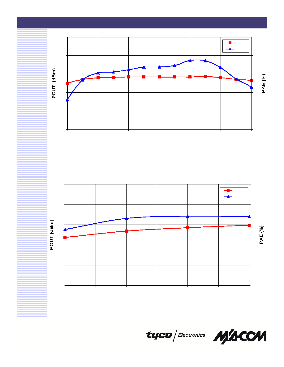
Figure 1. Output Power and Power Added Efficiency vs. Frequency at V
DD
= 8V
and P
in
= 12 dBm.
0
10
20
30
40
50
10
11
12
13
14
15
16
Frequency (GHz)
0
10
20
30
40
50
POUT
PAE
0
10
20
30
40
50
4
5
6
7
8
9
10
Drain Voltage (V)
0
10
20
30
40
50
POUT
PAE
Figure 2. Saturated Output Power and Power Added Efficiency vs. Drain Voltage at f
o
= 13 GHz.
RO-P-DS-3023 - -
4/6
0.5W X/Ku-Band Power Amplifier
MAAPGM0040-DIE
V 1.00
Specifications subject to change without notice.
Customer Service: Tel. (888)563-3949
Email: macom_adbu_ics@tycoelectronics.com
North America: Tel. (800) 366-2266
Asia/Pacific: Tel.+81-44-844-8296, Fax +81-44-844-8298
Europe: Tel. +44 (1344) 869 595, Fax+44 (1344) 300 020
Visit www.macom.com for additional data sheets and product information.
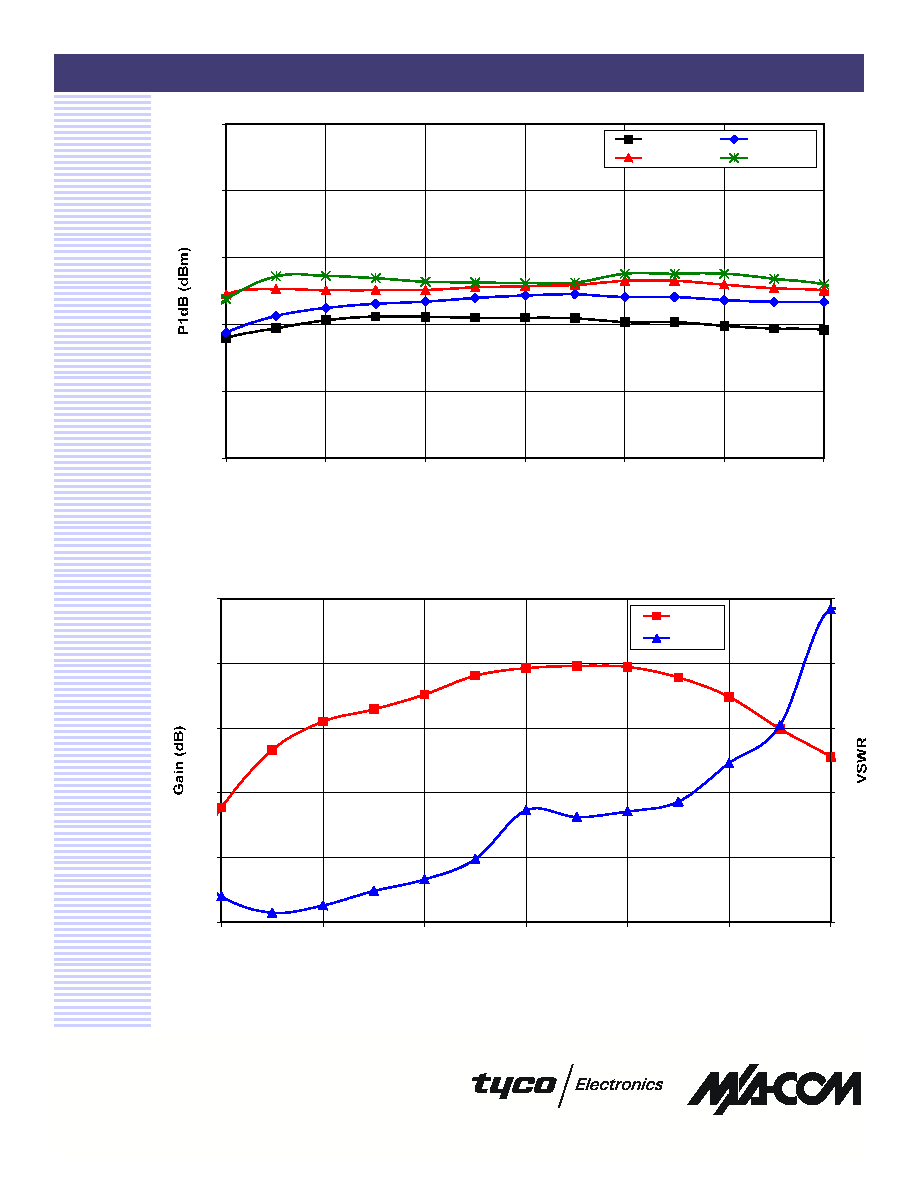
Figure 3. 1dB Compression Point vs. Drain Voltage
0
10
20
30
40
50
10
11
12
13
14
15
16
Frequency (GHz)
VDD = 4
VDD = 6
VDD = 8
VDD = 10
Figure 4. Small Signal Gain and Input VSWR vs. Frequency at V
DD
= 8V.
5
10
15
20
25
30
10
11
12
13
14
15
16
Frequency (GHz)
1
2
3
4
5
6
GAIN
VSWR
RO-P-DS-3023 - -
5/6
0.5W X/Ku-Band Power Amplifier
MAAPGM0040-DIE
V 1.00
Specifications subject to change without notice.
Customer Service: Tel. (888)563-3949
Email: macom_adbu_ics@tycoelectronics.com
North America: Tel. (800) 366-2266
Asia/Pacific: Tel.+81-44-844-8296, Fax +81-44-844-8298
Europe: Tel. +44 (1344) 869 595, Fax+44 (1344) 300 020
Visit www.macom.com for additional data sheets and product information.
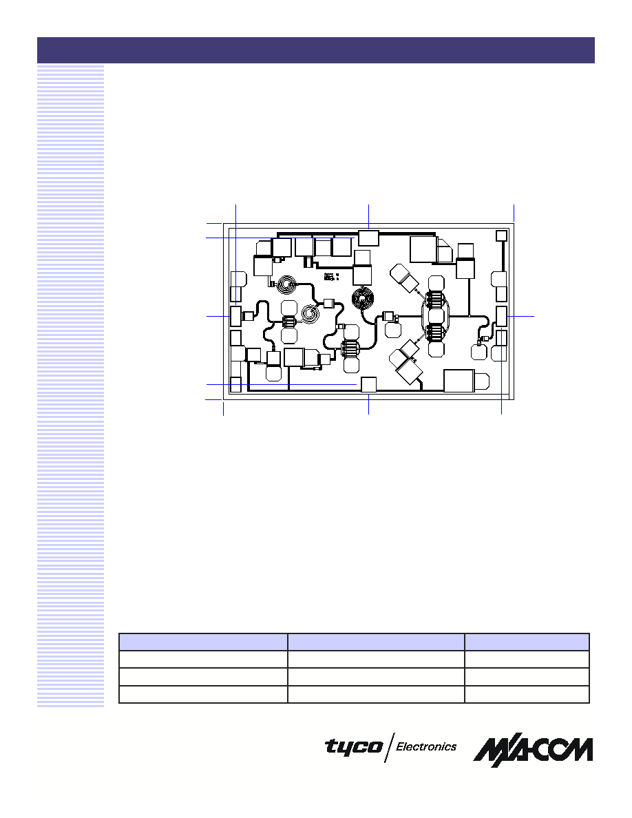
IN
V
GG
OUT
V
DD
V
DD
0.152 mm.
0.852 mm.
1.652 mm.
1.804 mm.
0.852 mm.
1.490 m
m
.
0
.
127 mm.
1
.
490 mm.
2
.
980 mm.
0
0
2.853 m
m
.
Mechanical Information
Chip Size: 2.980 x 1.804 x 0.075 mm
(
117 x 72 x 3 mils)
Pad
Size (
µm)
RF In and Out
100 x 200
DC Drain Supply Voltage VDD
200 x 150
DC Gate Supply Voltage VGG
150 x 150
Size (mils)
4 x 8
8 x 6
6 x 6
Bond Pad Dimensions
Figure 5. Die Layout
Chip edge to bond pad dimensions are shown to the center of the bond pad.