
1 Watt/2 Watt L-Band Power Amplifier
1.435 - 1.525 GHz
AM42
-
0054
OUTLINE DRAWING
1
V 1P.00
Preliminary
Features
·
High Linear Gain: 26 dB typ.
·
High Saturated Output Power: +33 dBm typ.
·
50 Ohm Input/Output Broadband Matched
Description
M/A-COM's AM42-0054 is a two stage MMIC power ampli-
fier in a bolt down ceramic package, allowing easy assembly.
The AM42-0054 employs a fully matched chip with internally
decoupled gate and drain bias networks. The AM42-0054 is
designed to operate from a constant current drain supply or a
constant voltage gate supply. By varying the bias conditions,
the saturated output power performance of this device may be
tailored for various applications.
The AM42-0054 is ideally suited for use as an output stage in
telemetry systems. The AM42-0054 includes internal supply
line bypassing in the package, minimizing the number of exter-
nal components required.
M/A-COM's AM42-0054 is fabricated using a mature 0.5-
micron MBE based GaAs MESFET process. The process fea-
tures full passivation for increased performance and reliability.
This product is 100% RF tested to ensure compliance to per-
formance specifications.
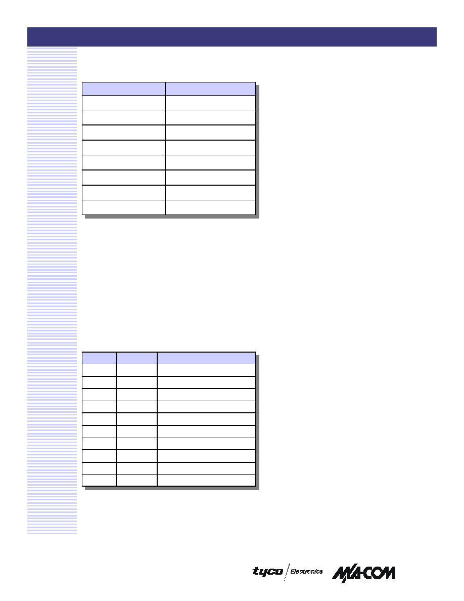
Electrical Specifications: V
DD
= +5V/+8V, V
GG
adjusted for Ids = 800 mA (with RF), Zo = 50
, T
A
= 25
°
C.
Parameter
Test Conditions
Frequency
Units
V
DD
= +5 V
(1 W operation)
V
DD
= +8 V
(2 W operation)
Linear Gain
Pin = -20 dBm,
Ids = 800 mA typ.
1.4 - 1.55 GHz
dB
25 typ.
25 typ.
Input VSWR
Pin = -20 dBm
1.4 - 1.55 GHz
Ratio
< 2.0:1
< 2.0:1
Output VSWR
Pin = -20 dBm
1.4 - 1.55 GHz
Ratio
< 2.0:1
< 2.0:1
Output Power (saturated)
Pin = +10 dBm
1.4 - 1.55 GHz
dBm
30 typ.
33 typ.
Output Power vs. Frequency
Pin = +10 dBm
1.4 - 1.55 GHz
dBm
±0.9 typ.
±0.4 typ.
Drain Bias Current
Pin = +10 dBm
1.4 - 1.55 GHz
mA
700 typ.
800 typ.
Gate Bias Voltage (V
GG
)
Pin = +10 dBm
1.4 - 1.55 GHz
V
-2.0 min; -0.4max
-2.0 min; -0.4max
Gate Bias Current (I
GG
)
Pin = +10 dBm
1.4 - 1.55 GHz
mA
25 typ.
25 typ.
Power Added Effiency
Pin = +10 dBm
1.4 - 1.55 GHz
%
37 typ.
29 typ.
CERAMIC
BASE PLATE
4X .06 X 45°
CHAMFER
6
5
4
3
2
1
7
8
9
10
.010 SQ.
ORIENTATION TAB
2X o .096 THRU
o.004 M
A B C
.090
MAX
.33
.005
± .002
.030
.318
± .010
.328
± .010
.050 MIN.
10X
.530
.70
.159
.010
± .003
10X
.040
.100
4X
.115
± .010
.050
4X
.085
- C -
- B -
- A -
Notes: (Unless Otherwise Specified)
1. Dimensions are in inches.
2. Tolerance: in .xxx =
±
.005
.xx =
±
.010
1.
Die available upon request (die size = 2970 x 2550 µm).
M/A-COM Inc. and its affiliates reserve the right to make changes to the product(s)
or information contained herein without notice. M/A-COM makes no warranty,
representation, or guarantee regarding the suitability of its products for any particular
purpose, nor does M/A-COM assume any liability whatsoever arising out of the use
or application of any product(s) or information.
Visit www.macom.com for additional data sheets and product information.
1 Watt / 2 Watt L-Band Power Amplifier
AM42-0054
V 1P.00
n
North America: Tel. (978) 656-2693
n
Asia/Pacific: Tel.+81-44-844-8296, Fax +81-44-844-8298
n
Europe: Tel. +44 (1344) 869 595, Fax+44 (1344) 300 020
2
Absolute Maximum Ratings
2,3,4,5,6
2.
Exceeding any one or a combination of these limits may
cause permanent damage.
3.
Adequate heat sinking and grounding required on flange
base.
4.
Apply -3 volts to pins 5 and 6 (V
GG
), prior to applying +8
volts to pins 1 or 10 (V
DD
). Adjust V
GG
for typical drain cur-
rent.
5.
For optimum IP3 performance, V
DD
bypass capacitors
should be placed within 0.5 inches of the V
DD
leads.
6.
DC blocks are required for RF input and output ports
Parameter
Absolute Maximum
Input Power
+12 dBm
V
DD
+10 volts
V
GG
-5 volts
V
DD
- V
GG
12 volts
Ids
1200 mA
Channel Temperature
+150
°
C
Operating Temperature
-40
°
C to +85
°
C
Storage Temperature
-65
°
C to +150
°
C
Pin Configuration
Pin No.
Pin Name Description
1
VD1
Drain Supply to First Stage
2
GND
DC and RF Ground
3
RF In
RF Input
4
GND
DC and RF Ground
5
VG1
Gate Supply to First Stage
6
VG2
Gate Supply to Second Stage
7
GND
DC and RF Ground
8
RF Out
RF Output
9
GND
DC and RF Ground
10
VD2
Drain Supply to Second Stage
M/A-COM Inc. and its affiliates reserve the right to make changes to the product(s)
or information contained herein without notice. M/A-COM makes no warranty,
representation, or guarantee regarding the suitability of its products for any particular
purpose, nor does M/A-COM assume any liability whatsoever arising out of the use
or application of any product(s) or information.
Visit www.macom.com for additional data sheets and product information.
1 Watt / 2 Watt L-Band Power Amplifier
AM42-0054
V 1P.00
n
North America: Tel. (978) 656-2693
n
Asia/Pacific: Tel.+81-44-844-8296, Fax +81-44-844-8298
n
Europe: Tel. +44 (1344) 869 595, Fax+44 (1344) 300 020
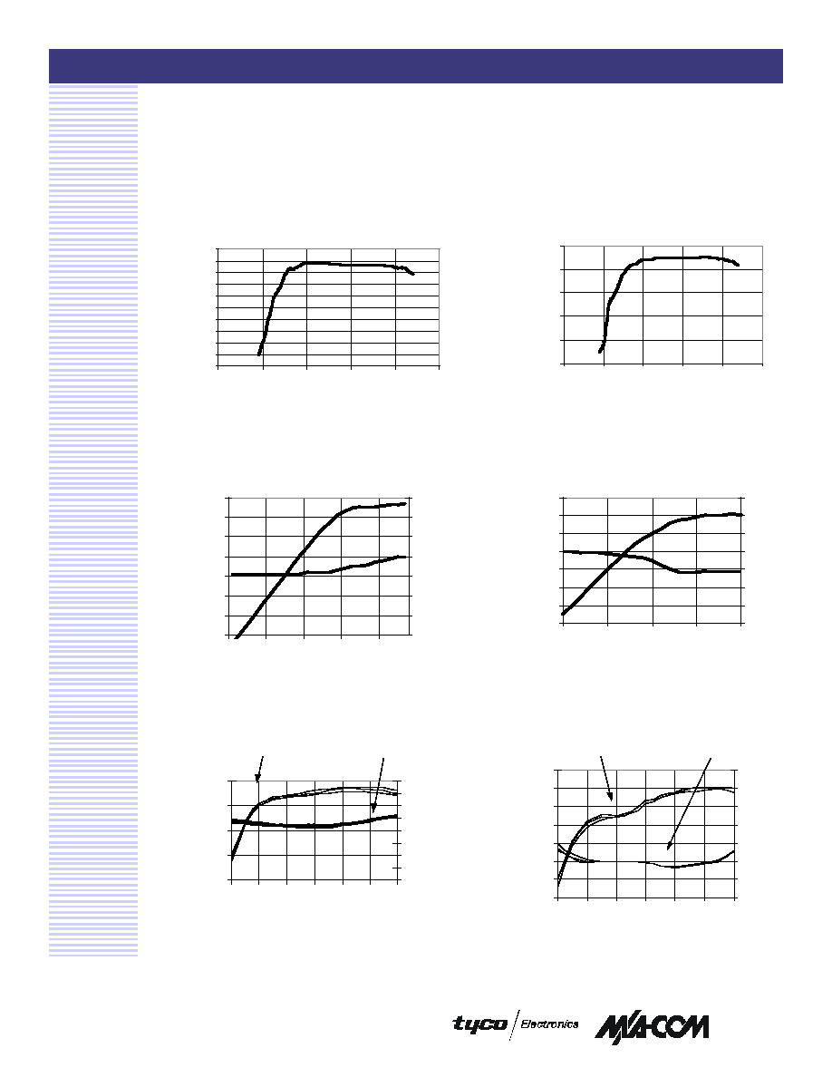
Typical Performance Curves
1 WATT PERFORMANCE
LINEAR GAIN VS FREQUENCY
2 WATT PERFORMANCE
LINEAR GAIN VS FREQUENCY
2 WATT PERFORMANCE
P
OUT
AND CURRENT VS P
IN
3
1 WATT PERFORMANCE
P
OUT
AND CURRENT VS P
IN
2 WATT PERFORMANCE
GAIN AND CURRENT VS FREQ.
1 WATT PERFORMANCE
GAIN AND CURRENT VS FREQ.
20
21
22
23
24
25
26
27
28
29
30
1
1.2
1.4
1.6
1.8
2
Frequency (GHz)
S21 (dB)
20
22
24
26
28
30
1
1.2
1.4
1.6
1.8
2
Frequency (GHz)
S21 (dB)
20
22
24
26
28
30
32
34
-10
-5
0
5
10
Power in (dBm)
Power out (dBm)
500
600
700
800
900
1000
1100
1200
Drain current (mA)
18
20
22
24
26
28
30
32
-10
-5
0
5
10
Power in (dBm)
Power out (dBm)
400
500
600
700
800
900
1000
1100
Drain current (mA)
26
28
30
32
34
1200 1300 1400 1500 1600 1700 1800
Frequency (MHz)
Power out (dBm)
400
500
600
700
800
900
1000
1100
1200Drain current (mA)
P
in
=7, 8.5,10dBm
I
DD
25
26
27
28
29
30
31
32
1200 1300 1400 1500 1600 1700 1800
Frequency (MHz)
Power out (dBm)
500
600
700
800
900
1000
1100
1200
Drain current (mA)
P
in
=7, 8.5,10dBm
I
DD

M/A-COM Inc. and its affiliates reserve the right to make changes to the product(s)
or information contained herein without notice. M/A-COM makes no warranty,
representation, or guarantee regarding the suitability of its products for any particular
purpose, nor does M/A-COM assume any liability whatsoever arising out of the use
or application of any product(s) or information.
Visit www.macom.com for additional data sheets and product information.
1 Watt / 2 Watt L-Band Power Amplifier
AM42-0054
V 1P.00
n
North America: Tel. (978) 656-2693
n
Asia/Pacific: Tel.+81-44-844-8296, Fax +81-44-844-8298
n
Europe: Tel. +44 (1344) 869 595, Fax+44 (1344) 300 020
Typical Performance Curves
1 WATT PERFORMANCE
LINEAR GAIN VS FREQUENCY
2 WATT PERFORMANCE
LINEAR GAIN VS FREQ AND TEMP
2 WATT PERFORMANCE
CURRENT VS TEMP AT 1.5 GHz
4
1 WATT PERFORMANCE
CURRENT VS TEMP AT 1.5 GHz
2 WATT PERFORMANCE
P
out
VS FREQ AND TEMP
1 WATT PERFORMANCE
P
out
VS FREQ AND TEMP
26
27
28
29
30
31
1.35
1.40
1.45
1.50
1.55
1.60
Frequency (GHz)
Linear Gain (dB)
26
27
28
29
30
31
1.35
1.40
1.45
1.50
1.55
1.60
Frequency (GHz)
Linear Gain (dB)
+85°C
+25°C
-20C
-40°C
+85°C
+25°C
-20C
-40°C
650
670
690
710
730
750
+85
+25
-20
-40
Temperature (C)
Current (mA)
740
760
780
800
820
840
860
+85
+25
-20
-40
Temperature (C)
Current (mA)
31.0
31.5
32.0
32.5
33.0
33.5
1.35
1.40
1.45
1.50
1.55
1.60
Frequency (GHz)
Output Power (dBm)
+85°C
+25°C
-20C
-40°C
28.0
28.5
29.0
29.5
30.0
30.5
31.0
1.35
1.40
1.45
1.50
1.55
1.60
Frequency (GHz)
Output Power (dBm)
+85°C
+25°C
-20C
-40°C

M/A-COM Inc. and its affiliates reserve the right to make changes to the product(s)
or information contained herein without notice. M/A-COM makes no warranty,
representation, or guarantee regarding the suitability of its products for any particular
purpose, nor does M/A-COM assume any liability whatsoever arising out of the use
or application of any product(s) or information.
Visit www.macom.com for additional data sheets and product information.
1 Watt / 2 Watt L-Band Power Amplifier
AM42-0054
V 1P.00
n
North America: Tel. (978) 656-2693
n
Asia/Pacific: Tel.+81-44-844-8296, Fax +81-44-844-8298
n
Europe: Tel. +44 (1344) 869 595, Fax+44 (1344) 300 020
Ordering Information
7
Part Number
Package
AM42-0054
CR-15 package
5
7.
Die available upon request.