
V2.00
GaAs MMIC VSAT Power Amplifier, 0.5W, 14.0-14.5 GHz
AM42-0041
M/A-COM Division of AMP Incorporated
s
North America: Tel. (800) 366-2266, Fax (800) 618-8883
s
Asia/Pacific: Tel.+85 2 2111 8088, Fax +85 2 2111 8087
s
Europe: Tel. +44 (1344) 869 595, Fax+44 (1344) 300 020
www.macom.com
AMP and Connecting at a Higher Level are trademarks.
Specifications subject to change without notice.
Ordering Information
Part Number
Package
AM42-0041
Ceramic Bolt Down Package
Electrical Specifications:
T
A
= +25°C, V
DD
= +8V, V
GG
adjusted for Ids = 500 mA, Z
0
= 50
,
F = 14.0 - 14.5 GHz
Parameter
Abbv.
Test Conditions
Units
Min.
Typ.
Max.
Linear Gain
G
L
P
IN
-10 dBm
dB
27
28
--
Input VSWR
VSWR
IN
P
IN
-10 dBm
--
--
2.5:1
2.7:1
Output VSWR
VSWR
OUT
P
IN
-10 dBm
--
--
2.5:1
--
Saturated Output Power
P
SAT
P
IN
=
+3 dBm, I
DD
=500 mA Typ.
dBm
27.0
28.0
29.0
Output Power Flatness vs.
Frequency
P
SAT
P
IN
=
+3 dBm, I
DD
=500 mA Typ.
dB
--
1.0
1.5
Output Power vs. Temperature
(with respect to T
A
=+25°C)
P
SAT
P
IN
=
+3 dBm, I
DD
=500 mA Typ.
T
A
= -40°C to +70°C
dB
--
±0.4
--
Noise Figure
NF
P
IN
-10 dBm, I
DD
=500 mA Typ.
dB
--
7
--
Drain Bias Current
I
DD
P
IN
=
+3 dBm
mA
400
500
600
Gate Bias Voltage
V
GG
P
IN
=
+3 dBm, I
ds
=500 mA Typ.
V
-2.4
-1.0
-0.4
Gate Bias Current
GG
P
IN
=
+3 dBm, I
ds
=500 mA Typ.
mA
--
5
15
Thermal Resistance
JC
25°C Heat Sink
°C/W
--
9.5
--
Power Added Efficiency
PAE
P
IN
=
+3 dBm, I
ds
=500 mA Typ.
%
--
22
--
CR-15
Features
·
High Linear Gain: 28 dB Typ.
·
High Saturated Output Power: +28 dBm Typ.
·
High Power Added Efficiency: 22% Typ.
·
50
Input/Output Broadband Matched
·
High Performance Ceramic Bolt Down Package
Description
M/A-COM's AM42-0041 is a four-stage MMIC linear power
amplifier in a ceramic bolt down style hermetic package. The
AM42-0041 employs a fully matched chip with internally decou-
pled Gate and Drain bias networks. The AM42-0041 is designed
to be operated from a constant current Drain supply. By varying
the Gate bias voltage, the saturated output power performance of
this device can be tailored for various applications.
The AM42-0041 is ideally suited for use as an output stage or a
driver, in applications for VSAT systems. This design is fully
monolithic and requires a minimum of external components.
M/A-COM's AM42-0041 is fabricated using a mature 0.5 mi-
cron MBE based GaAs MESFET process. The process features
full passivation for increased performance and reliability. This
product is 100% RF tested to ensure compliance to performance
specifications.
GaAs MMIC VSAT Power Amplifier, 0.5W
14.0 - 14.5 GHz
AM42-0041
Notes: (unless otherwise specified)
1. Dimensions are in inches.
2. Tolerance: .XXX = ± 0.005
.XX = ± 0.010
V2.00
GaAs MMIC VSAT Power Amplifier, 0.5W, 14.0-14.5 GHz
AM42-0041
M/A-COM Division of AMP Incorporated
s
North America: Tel. (800) 366-2266, Fax (800) 618-8883
s
Asia/Pacific: Tel.+85 2 2111 8088, Fax +85 2 2111 8087
s
Europe: Tel. +44 (1344) 869 595, Fax+44 (1344) 300 020
www.macom.com
AMP and Connecting at a Higher Level are trademarks.
Specifications subject to change without notice.
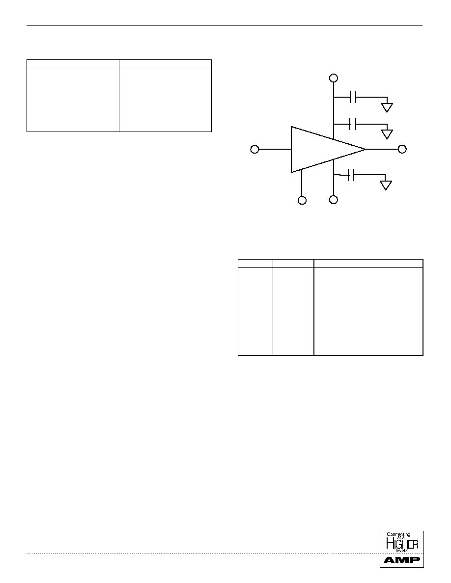
Typical Bias Configuration
3,4,7
Absolute Maximum Ratings
1,2,3,4
Parameter
Absolute Maximum
Input Power
+23 dBm
V
DD
+12 Volts
V
GG
-3 Volts
V
DD
- V
GG
12 Volts
I
ds
1000 mA
Channel Temperature
-40°C to +85°C
Storage Temperature
-65°C to +150°C
1. Operation of this device outside any of these limits may cause
permanent damage.
2. Case Temperature (T
C
) = +85°C.
3. Nominal bias is obtained by first connecting -2.4 volts to pin 5 or
pin 6 (V
GG
), followed by connecting +8 volts to pin 1 or pin 10
(V
DD
). Note sequence. Adjust V
GG
for a drain current of 500 mA
typical.
4. RF ground and thermal interface is the flange (case bottom).
Adequate heat sinking is required.
5. No dc bias voltage appears at the RF ports.
6. The dc resistance at the input and output ports is a short circuit. No
voltage is allowed on these ports.
7. For optimum IP
3
performance, the V
DD
bypass capacitors should be
placed within 0.5 inches of the V
DD
leads.
Pin No.
Pin Name
Description
1
V
DD
Drain Supply
2
GND
DC and RF Ground
3
RF In
RF Input
4
GND
DC and RF Ground
5
V
GG
Gate Supply
6
V
GG
Gate Supply
7
GND
DC and RF Ground
8
RF Out
RF Output
9
GND
DC and RF Ground
10
V
DD
Drain Supply
Pin Configuration
AM42-0041
µ
F
3.3
µ
F
0.01
µ
F
1.0
3
RF IN
RF OUT
8
1 or 10
V
DD
V
GG
GND
2,4,7,9
5 or 6
V2.00
GaAs MMIC VSAT Power Amplifier, 0.5W, 14.0-14.5 GHz
AM42-0041
M/A-COM Division of AMP Incorporated
s
North America: Tel. (800) 366-2266, Fax (800) 618-8883
s
Asia/Pacific: Tel.+85 2 2111 8088, Fax +85 2 2111 8087
s
Europe: Tel. +44 (1344) 869 595, Fax+44 (1344) 300 020
www.macom.com
AMP and Connecting at a Higher Level are trademarks.
Specifications subject to change without notice.
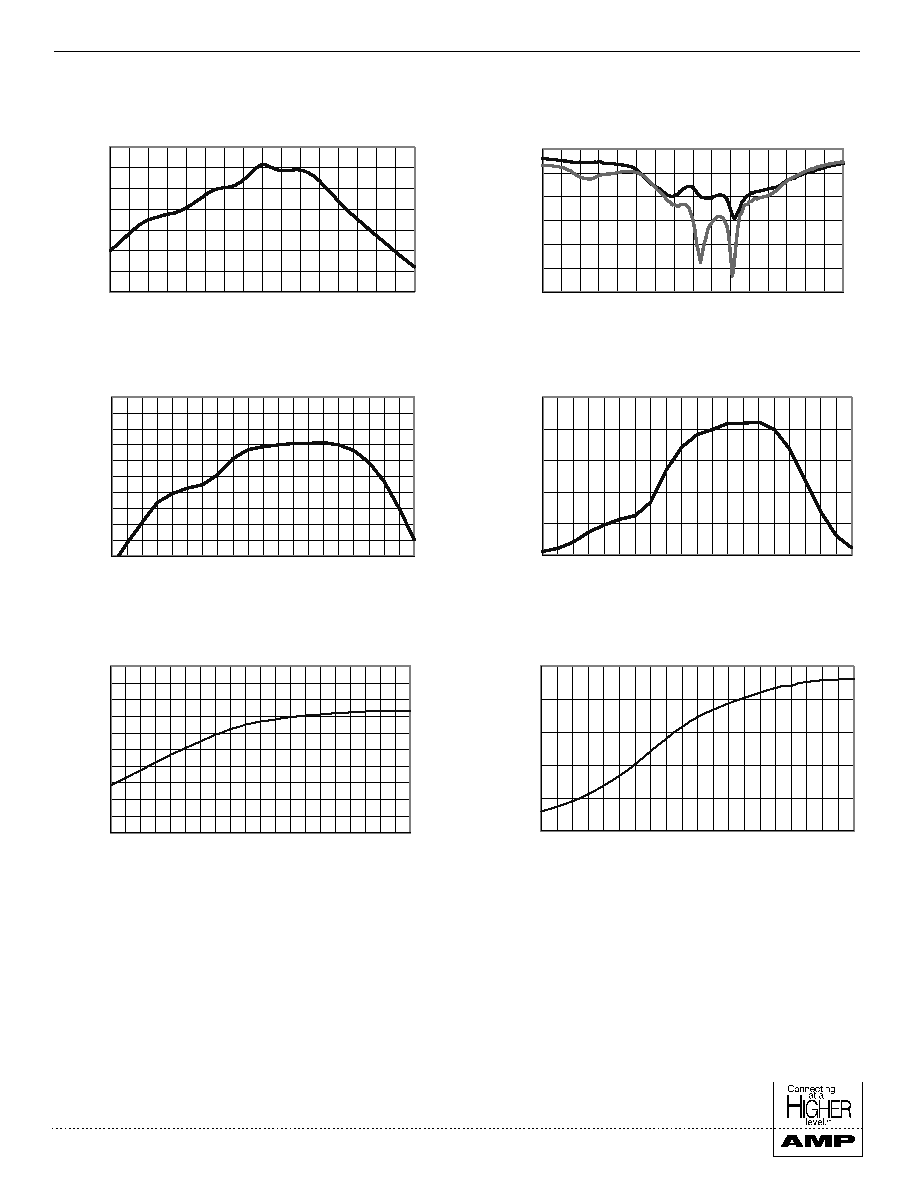
Typical Performance @ +25°C
-30
-20
-10
0
10
20
30
40
10.0
10.5
11.0
11.5
12.0
12.5
13.0
13.5
14.0
14.5
15.0
15.5
16.0
16.5
17.0
17.5
18.0
Frequency (GHz)
Linear Gain (dB)
-30
-25
-20
-15
-10
-5
0
10.0
10.5
11.0
11.5
12.0
12.5
13.0
13.5
14.0
14.5
15.0
15.5
16.0
16.5
17.0
17.5
18.0
Frequency (GHz)
Magnitude (dB)
S11
S22
15
17
19
21
23
25
27
29
31
33
35
12.0
12.4
12.8
13.2
13.6
14.0
14.4
14.8
15.2
15.6
16.0
Frequency (GHz)
P
OUT
(dBm)
Output Power vs Frequency
@ P
IN
= +3 dBm
15
17
19
21
23
25
27
29
31
33
35
-10-9 -8 -7 -6 -5 -4 -3 -2 -1 0 1 2 3 4 5 6 7 8 9 10
P
IN
(dBm)
P
OUT
(dBm)
Output Power vs. Input Power
F = 14.25 GHz
0
5
10
15
20
25
12.0
12.4
12.8
13.2
13.6
14.0
14.4
14.8
15.2
15.6
16.0
Frequency (GHz)
PAE (%)
Power Added Efficiency (PAE) vs Frequency
@ P
IN
= +3 dBm
0
5
10
15
20
25
-10 -9 -8 -7 -6 -5 -4 -3 -2 -1 0 1 2 3 4 5 6 7 8 9 10
P
IN
(dBm)
PAE (%)
Power Added Efficiency (PAE) vs. Input Power
F = 14.25 GHz
Linear Gain vs. Frequency
Input and Output Return Loss vs. Frequency

V2.00
GaAs MMIC VSAT Power Amplifier, 0.5W, 14.0-14.5 GHz
AM42-0041
M/A-COM Division of AMP Incorporated
s
North America: Tel. (800) 366-2266, Fax (800) 618-8883
s
Asia/Pacific: Tel.+85 2 2111 8088, Fax +85 2 2111 8087
s
Europe: Tel. +44 (1344) 869 595, Fax+44 (1344) 300 020
www.macom.com
AMP and Connecting at a Higher Level are trademarks.
Specifications subject to change without notice.