June 2000
1
Copyright © 1999, 2000 by LSI Logic Corporation. All rights reserved.
MiniRISC
®
EZ4021-FC
EasyMACRO Microprocessor
Preliminary Datasheet
The MiniRISC EZ4021-FC Microprocessor EasyMACRO is a compact,
high-performance, 64-bit microprocessor subsystem implemented in
G12TM CMOS technology. The EZ4021-FC uses the LSI Logic
CoreWare
®
system-on-a-chip methodology and executes the MIPS III
instruction set. It is ideal for high-performance, cost-sensitive embedded
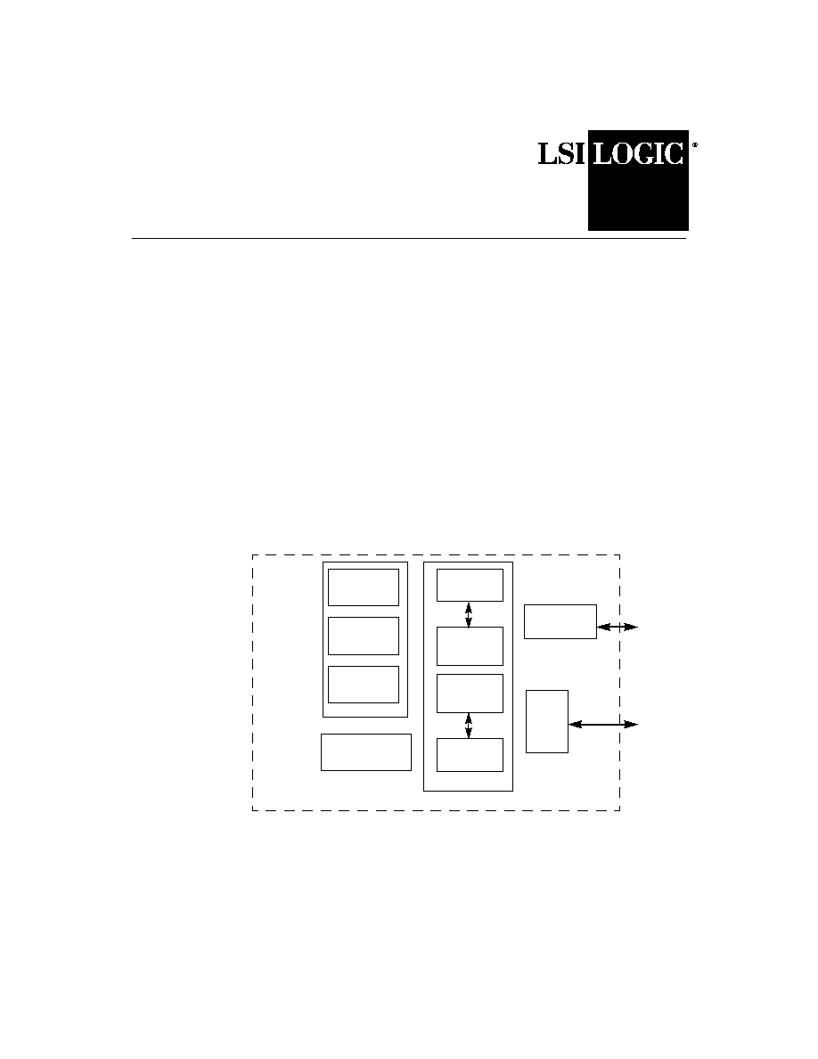
processor applications. As shown in
Figure 1
, the EZ4021-FC includes
the following components:
Figure 1
EZ4021-FC Microprocessor EasyMACRO Block
Diagram
·
CPU includes system
coprocessor, an integer data
path with multiply divide unit,
and a master pipeline
controller
·
Instruction and data caches
·
Memory Management Unit
(MMU)
·
Bus Interface Unit (BIU)
·
Quick Bus interface
·
EJTAG Interface module
CPU
Coprocessor 0
(CP0)
Integer Data
Path
(IDP)
Master Pipeline
Control
(MPC)
Instruction
Cache
Data
Cache
Caches
Memory
Management Unit
(MMU)
Bus
Interface
Unit
(BIU)
Quick Bus
Optional
Modules
EJTAG
JTAG
EZ4021-FC
Interface
Instruction
Cache
Controller
Data
Cache
Controller
EasyMACRO
ez4021ds.fm Page 1 Friday, May 26, 2000 8:27 AM

2
MiniRISC
®
EZ4021-FC EasyMACRO Microprocessor
Features
·
High-performance RISC CPU
Single issue, five-stage pipeline
250 native MIPS, 275 Dhrystone
MIPS at 250 MHz
250 MHz operation at WCABS (Tj =
125
°
C, VDD = 1.71V, WC process)
Both big- and little-endian support
for load and store operations
R4000 standard 32-bit
timer/counter
MIPS CPU standard interrupt
exceptions (one NMI, one timer,
five hardware, two software)
·
Integrated multiply and divide unit
High-performance eight bit/cycle
multiplier
32-bit signed/unsigned multiply
in five CPU clock cycles
64-bit signed/unsigned multiply
in nine CPU clock cycles
Compact one bit/cycle divider
32-bit signed/unsigned divide in
34 CPU clock cycles
64-bit signed/unsigned divide in
66 CPU clock cycles
·
Windows CE compatible MMU with 32
dual-entry page translations
·
Integrated instruction and data caches
Harvard architecture
16 Kbyte 2-way set-associative
instruction and data caches
LRU algorithm for replacement
Line level lock for instruction
RAM and scratchpad memory
Data cache has write-through or
write back update policy,
programmable on a page basis
·
MIPS III Instruction Set Architecture
MIPS III ISA supporting 64-bit
integer operations
Thirty-two 64-bit general-purpose
registers
R4000-style status register and
exception processing
Wait for Interrupt (WAITI) instruction
for power saving
Supports SPECIAL2 Multiply-
Accumulate extensions
·
Advanced Debug Support
MIPS EJTAG version 1.5.3
Instruction and data breakpoints
Program Counter (PC) trace
Processor singlestep and software
debug breakpoints
ez4021ds.fm Page 2 Friday, May 26, 2000 8:27 AM

MiniRISC
®
EZ4021-FC EasyMACRO Microprocessor
3
Features continued
Functional Description
The EZ4021-FC CPU performs all arithmetic, logical, shift, and address
calculations. The CPU includes:
·
Data path and control
Contains a 64-bit integer data path module with a 32 x 64-bit register
file and an instruction decoder/data path control module.
·
Integrated Multiply/Divide Unit (MDU)
Supports the MIPS accumulate operations (MADD, MADDU, MSUB,
and MSUBU) and the three-operand multiply (MUL). The MDU
includes an eight-bits-per-cycle multiply capability and a one-bit-per-
cycle divide capability.
·
System control coprocessor (CP0)
Provides exception processing support using the MIPS R4000
exception model and processor state control that includes three
operating modes--kernel, user, supervisor.
The EZ4021-FC interface supports a new high-performance, on-chip bus
known as the Quick Bus. The Quick Bus is a split-transaction bus that
allows the overlap of memory requests (fetch/load/store) and data
returns. A Quick Bus design operating at 125 MHz can achieve a peak
bandwidth of 1.0 Gbytes per second.
The Bus Interface Unit (BIU) passes address/data between the CPU and
the Quick Bus and arbitrates CPU-to-Quick Bus access. It provides a 64-
bit incoming datapath from the Quick Bus to the CPU and a 64-bit path
for outgoing data. Depending on the customer design, outgoing Quick
Bus data can go to a variety destinations outside the EZ4021-FC.
·
Technology
2.6 mW/MHz power consumption
(includes caches)
12 mm
2
core size
1.8 V Core VDD
LSI Logic G12 CMOS technology
(0.18
µ
L-drawn, 0.15
µ
L-effective)
ez4021ds.fm Page 3 Friday, May 26, 2000 8:27 AM

4
MiniRISC
®
EZ4021-FC EasyMACRO Microprocessor
The EZ4021-FC has separate instruction and data caches (I-Cache and
D-Cache). Each cache is organized as a two-way set associative
16 Kbyte cache with a fixed cache block (line) size of 8 words (32-bytes).
The caches are virtually indexed and physically tagged.
The memory management unit (MMU) performs virtual-to-physical
address translation using a 32-entry joint translation lookaside buffer
(TLB). The MMU supports a variety of page sizes from 4 Kbytes to
1 Mbyte.
The EZ4021-FC includes a Joint Test Action Group (JTAG) interface and
supports Enhanced JTAG (EJTAG) functions. EJTAG is a debug feature
of MIPS-based processors. You can use EJTAG to debug stand-alone
processors as well as 32-bit or 64-bit processors that are embedded in
a system like the EZ4021-FC.
Pipeline Architecture
The EZ4021-FC five-stage instruction pipeline is illustrated in
Figure 2
.
Figure 2
EZ4021-FC Instruction Pipeline
Instruction fetch occurs during the first two pipeline stages and
instruction execution during the last three stages. After a stage accepts
an instruction from the previous stage, it must hold the instruction for
re-execution in case the pipeline stalls. The function of each pipeline
stage is summarized below.
Instruction Fetch (I) The EZ4021-FC fetches the instruction during
this first stage.
Register Read (R) In the R stage, the CPU reads any required
operands from the Register File while decoding the instruction.
Instruction Fetch
Instruction Execution
X
M
R
I
W
ez4021ds.fm Page 4 Friday, May 26, 2000 8:27 AM

MiniRISC
®
EZ4021-FC EasyMACRO Microprocessor
5
Execute (X) Computational and logical instructions execute during the
X stage. The CPU resolves conditional branches during this stage, and
does the address calculations for load and store instructions.
Memory Access (M) In this stage, the CPU accesses the cache for
load and store instructions. Data returns to the register bypass logic at
the end of the M stage.
Write Back (W) The CPU writes results into the Register File in the W
stage.
Application Examples
The EZ4021-FC is designed for mid- to high-end applications, including
set top boxes and image-processing engines, networking
switches/routers, and consumer products requiring 64-bit performance.
CoreWare Program
The CoreWare program consists of three main elements:
1.
A library of cores
2.
A design development and simulation package
3.
Expert applications support
The CoreWare library contains a wide range of complex cores based on
accepted and emerging industry standards from high-speed interconnect
and digital video to DSP and MIPS microprocessors. LSI Logic provides
a complete framework for device and system development and
simulation. LSI Logic has advanced ASIC technologies that consistently
produce Right-First-TimeTM silicon. The LSI Logic in-house experts
provide design support from system architecture definition through chip
layout and test vector generation.
ez4021ds.fm Page 5 Friday, May 26, 2000 8:27 AM